

Page 1
MA28151
1/22
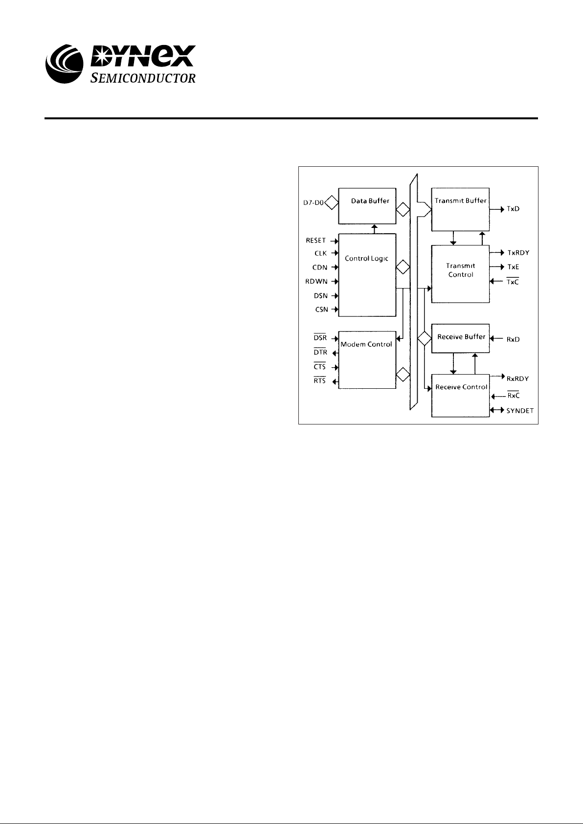
Figure 1: MA28151 Block Diagram
The MA28151 is based on the industry standard 8251A
Universal Synchronous Asynchronous Receiver/Transmitter
(USART), modified for data communications with the MAS281
microprocessor.
The MA28151 is used as a peripheral device and is
programmed by the CPU to operate using virtually any serial
data transmission technique presently in use (including IBM
“bi-sync”). The USART accepts data characters from the CPU
in parallel format and then converts them into a continuous
serial data stream for transmission.
Simultaneously, it can receive serial data streams and
convert them into parallel data characters for the CPU. The
USART signals the CPU whenever it receives a character for
transmission or whenever it receives a character for the CPU.
The CPU can read the complete status of the USART at any
time, including data transmission errors and control signals
such as SYNDET and TxEMPTY.
FEATURES
■ Radiation Hard to 1MRad(Si)
■ Latch Up Free, High SEU Immunity
■ Silicon-on-Sapphire Technology
■ Synchronous 5 - 8 Bit Characters; Internal or External
Character Synchronisation; Automatic Sync Insertion
■ Asynchronous 5 - 8 Bit Characters; Clock Rate - 1, 16 or
64 Times Baud Rate; Break Character Generation, 1
1
⁄2 or
2 Stop Bits
■ All Inputs and Outputs are TTL Compatible
■ Compatible with the MAS281 (MIL-STD-1750A)
Microprocessor
The MA28151 is based on the industry standard 8251A
USART, modified for use with the MAS281 processor,
incorporating the following features:
1. MA28151 has double-buffered data paths with separate l/O
registers for control status, data in and data out, which
considerably simplifies control programming and minimizes
CPU overhead.
2. In synchronous operations, the Receiver detects and
handles “break” automatically, relieving the CPU of this task.
3. A refined Rx initialisation prevents the Receiver from
starting when in the “break” state, preventing unwanted
interrupts from the disconnected USART.
4. At the conclusion of a transmission, the TxD line will always
return to the marking state unless SBRK is programmed.
5. Tx Enable logic enhancement prevents a Tx Disable
command from prematurely halting transmission of the
previously written data before completion. The logic also
prevents the transmitter from turning off in the middle of a
word.
6. When external Sync Detect is programmed, Internal Sync
Detect is disabled and an External Sync Detect status is
provided via a flip-flop, which clears itself upon a status read.
7. The possibility of a false sync detect is minimized in two
ways: by ensuring that if double character sync is
programmed, the characters will be continuously detected and
by clearing the Rx register to all 1’s whenever Enter-Hunt
command is issued in Sync mode.
8. When the MA28151 is not selected, the RDWN and DSN
lines do not affect the internal operation of the device.
9. The MA28151 Status can be read at any time but the status
update will be inhibited during status read.
10. The MA28151 is free from extraneous glitches, providing
higher speed and better operating margins.
11. Synchronous Baud rate is from DC to 64K.
12. Asynchronous Baud rate is from DC to 19.2K.
MA28151
Radiation hard Programmable
Communication Interface
Replaces Jone 1999 version, DS3574-4.0 DS3574-5.0 January 2000
Page 2

MA28151
2/22
1. FUNCTIONAL DESCRIPTION
1.1 GENERAL
The MA28151 is a Universal Synchronous/Asynchronous
Receiver/Transmitter designed for use with the MAS281
microprocessor. Like other l/O devices in a microcomputer
system, its functional configuration is programmed by the
system’s software for maximum flexibility. The MA28151 can
support most serial data techniques in use, including IBM bisync.
In a communication environment, an interface device must
convert parallel format system data into serial format for
transmission, and convert incoming serial data into parallel
system data for reception. The interface device must also
delete or insert bits or characters that are functionally unique to
the communication technique. In essence, the interface should
appear transparent to the CPU for the simple input or output of
byte-oriented system data.
1.2 DATA BUS BUFFER
This 3-state, bidirectional, 8-bit buffer is used to interface
the MA28151 to the system data bus. Data is transmitted or
received by the buffer upon execution of OUTput or INput
instructions from the CPU.
Control word, Command words and Status information are
also transferred through the Data Bus Buffer. The Command
Status, Data-in and Data-out registers are separate 8-bit
registers, communicating with the system bus through the
Data Bus Buffer.
This functional block accepts inputs from the system
control bus and generates control signals for overall device
operation. It contains the Control Word Register and
Command Word Register, which store the various control
formats for the device’s functional definition.
1.3 RESET
A high on this input forces the MA28151 into idle mode.
The MA28151 will remain at idle until its functional definition is
programmed with a new set of control words. Minimum RESET
pulse width is 6 tcy (clock must be running).
The device can also be put into the idle state by a
command reset operation .
1.4 CLOCK (CLK)
The CLK input is used to generate internal device timing
and is normally connected to the clock generator (OSC) of the
system.
Please note: None of the external inputs or outputs are
referenced to CLK but the frequency of CLK must be greater
than 30 times the Receiver or Transmitter data bit rates.
1.5 DATA STROBE (DSN)
This input indicates that a data transfer is taking place.
During a CPU write operation the MA28151 reads data from
the bus on the rising edge of DSN. During a read operation the
MA28151 can output data while DSN is low. Data is valid on
the rising edge of DSN.
1.6 READ/WRITE SELECT (RDWN)
A high on the RDWN input indicates a read of data or
status information from the MA28151. A low on this input
indicates a transfer of data or control words into the MA28151.
The RDWN line is valid only when DSN is low. Figure 2
summarises the MAS28151 read/write operati ons.
1.7 CONTROL/DATA (CDN)
This input, in conjunction with the DSN and RDWN inputs,
informs the MA28151 that the word on the Data Bus is either a
data character, control word or status information.
1 = CONTROL/STATUS; 0= DATA
CDN RDWN DSN CSN ACTION
0 1 0 0 28151 TO CPU
0 0 0 0 CPU TO 28151
1 1 0 0 STATUS TO CPU
1 0 0 0 CPU TO CONTROL
x x 1 0 BUS TRISTATE
x x x 1 BUS TRISTATE
Figure 2: Read/Write Control
1.8 CHIP SELECT (CSN)
A low on this input selects the MA28151. No reading or
writing will occur unless the device is selected. When CSN is
high, the Data Bus is in the float state and the DSN and RDWN
lines have no effect on the chip.
1.9 MODEM CONTROL
The MA28151 has a set of control inputs and outputs which
can be used to simplify the interface to almost any modem.
The modem control signals are general purpose in nature and
can be used for functions other than modem control, if
necessary.
1.10 DATA SET READY (
DSR)
The DSR input signal is a general-purpose, 1-bit inverting
input port. Its condition can be tested by the CPU using a
Status Read operation. The DSR input is normally used to test
modem conditions such as Data Set Ready.
1.11 DATA TERMINAL READY (
DTR)
The DTR output signal is a general purpose, 1-bit inverting
output port. It can be set low by programming the appropriate
bit in the Command instruction word. The DTR output signal is
normally used for modem control such as Data Terminal
Ready.
Page 3

MA28151
3/22
1.12 REQUEST TO SEND (
RTS)
The RTS output signal is a general purpose, 1-bit inverting
output port. It can be set low by programming the appropriate
bit in the Command instruction word. The RTS output signal is
normally used for modem control such as Request To Send.
1.13 CLEAR TO SEND (
CTS)
A low on this input enables the MA28151 to transmit serial
data if the Tx Enable bit in the Command byte is set to a high.
If either a Tx Enable off or
CTS off condition occurs while the
Tx is in operation, the Tx will transmit all the data in the
USART, written prior to Tx disable command, before shutting
down.
1.14 TRANSMITTER BUFFER
The Transmitter Buffer accepts parallel data from the Data
Bus Buffer, converts it to a serial bit stream, inserts the
appropriate characters or bits (based on the communication
technique) and outputs a composite serial stream of data on
the TxD output pin on the falling edge of
TxC. The transmitter
will begin transmission upon being enabled if CTS = 0. The
TxD line will be held in the marking state immediately upon a
master Reset, or when Tx Enable or CTS = 1, or the
transmitter is empty.
1.15 TRANSMITTER CONTROL
The Transmitter Control manages all activities associated
with the transmission of serial data. It accepts and issues
signals both externally and internally to accomplish this
function.
1.16 TRANSMITTER READY (TxRDY)
This output signals the CPU that the transmitter is ready to
accept a data character. The TxRDY output pin can be used as
an interrupt to the system since it is masked by TxEnable; or,
for Polled operation, the CPU can check TxRDY using a Status
Read operation. TxRDY is automatically reset by the falling
edge of DSN (with RDWN low) when a data character is
loaded from the CPU.
Note that when using the polled operation, the TxRDY
status bit is not masked by TxEnable, but will only indicate the
Empty/Full Status of the Tx Data input Register.
1.17 TRANSMITTER EMPTY (TxE)
When the MA28151 has no characters to send, the
TxEMPTY output will go high. It resets upon receiving a
character from CPU if the transmitter is enabled. TxEMPTY
remains high when the transmitter is disabled. TxEMPTY can
be used to indicate the end of transmission mode, so that the
CPU can turn the line around in the half-duplex operational
mode.
In the Synchronous mode, a high on the TxEMPTY output
indicates that a character has not been loaded and the SYNC
character or characters are about to be or are being
automatically transmitted as fillers. TxEMPTY does not go low
when the SYNC characters are being shifted out.
1.18 TRANSMITTER CLOCK
(TxC)
The Transmitter Clock controls the rate at which the
character is to be transmitted. In the Synchronous
transmission mode, the Baud Rate (1x) is equal to the TxC
frequency. In Asynchronous transmission mode, the baud rate
is a fraction of the actual TxC frequency. A portion of the mode
instruction selects this factor; it can be 1,1/16 or 1/64 the TxC.
For Example:
If Baud Rate equals 110 Baud
TxC equals 110Hz in the 1x mode
TxC equals 1 72KHz in the 16x mode
TxC equals 7.04KHz in the 64x mode
The falling edge of TxC shifts the serial data out of the
MA28151.
1.19 RECEIVER BUFFER
The Receiver accepts serial data, converts the data to
parallel format, checks for bits or characters that are unique to
the communications techniques and sends an assembled
character to the CPU. Serial data is input to the RxD pin and is
clocked in on the rising edge of RxC.
1.20 RECEIVER CONTROL
This functional block manages all receiver-related activities
which consist of the following features:
The RxD initialisation circuit prevents the MA28151 from
mistaking an unused input line for an active low data line in the
break condition. Before starting to receive serial characters on
the RxD line, a valid 1 must first be detected after a chip master
Reset. Once this has been determined, a search for a valid low
(start bit) is enabled. This feature is only active in the
asynchronous mode and is only done once for each master
Reset.
The False Start bit detection circuit prevents false starts as
the result of a transient noise spike by first detecting the falling
edge and then strobing the nominal center of the Start bit (RxD
= low).
Parity error detection sets the corresponding status bit.
The Framing Error status bit is set if the Stop bit is absent
at the end of the data byte (asynchronous mode).
1.21 RxRDY (RECEIVER READY)
This output indicates that the MA28151 contains a
character that is ready to be input to the CPU. RxRDY can be
connected to the interrupt structure of the CPU or, for polled
operation, the CPU can check the condition of RxRDY using a
Status Read operation. RxEnable, when off holds RxRDY in
the Reset Condition. For Asynchronous mode, to set RxRDY,
the Receiver must be enabled to sense a Start Bit and a
complete character must be assembled and transferred to the
Data Output Register. For Synchronous mode, to set RxRDY,
Page 4

MA28151
4/22
the Receiver must be enabled and a character must finish
assembly and be transferred to the Data Output Register
Failure to read the received character from the Rx Data
Output Register prior to the assembly of the next Rx Data
character will set overrun condition error and the previous
character will be written over and lost. If the Rx Data is being
read by the CPU when the internal transfer is occurring, the
overrun error will be set and the old character will be Iost.
1.22
RxC (RECEIVER CLOCK)
The Receiver Clock controls the rate at which the character
is to be received. In Synchronous Mode the Baud Rate (1x) is
equal to the actual frequency of
RxC. In Asynchronous Mode,
the Baud Rate is a fraction of the actual RxC frequency. A
portion of the mode instruction selects this factor: 1,1⁄16 or 1⁄64 of
the Receiver Clock.
For example:
Baud Rate equals 300 Baud, if
RxC equals 300 Hz in the 1 x mode:
RxC equals 4800 Hz in the 16x mode
RxC equals 19.2 KHz in the 64x mode.
Baud Rate equals 2400 Baud if
RxC equals 2400Hz in the 1x mode
RxC equals 38.4 KHz in the 16x mode;
RxC equals 153.6 KHz in the 64x mode.
Data is sampled into the MA28151 on the rising edge of RxC.
Note: In most communications systems, the MA28151 will
be handling both the transmission and reception operations of
a single link. Consequently the Receive and Transmit Baud
Rates will be the same. Both
TxC and RxC will require identical
frequencies for this operation and can be tied together and
connected to a single frequency source (Baud Rate
Generator) to simplify the interface.
1.23 SYNC/BREAK DETECT (SYNDET/BRKDET)
This pin is used in Synchronous Mode for SYNDET and
may be used as either input or output, programmable through
the Control Word. It is reset to output mode, low upon RESET.
When used as an output (internal Sync mode), the SYNDET
pin will go high to indicate that the MA28151 has located the
SYNC character in the Receive mode. If the MA28151 is
programmed to use double Sync characters (bi-sync), the
SYNDET will go high in the middle of the last bit of the second
Sync character.
SYNDET is automatically reset upon a Status Read
operation.
When used as an input (external SYNC detect mode), a
positive going signal will cause the MA28151 to start
assembling data characters on the rising edge of the next
RxC.
Once in SYNC, the high input signal can be removed. When
External SYNC Detect is programmed, Internal SYNC Detect
is disabled.
1.24 BREAK (ASYNC MODE ONLY)
This output will go high whenever the receiver remains low
through two consecutive stop bit sequences including the start
bits, data bits, and parity bits. Break Detect may also be read
as a Status bit. It is reset only upon a master chip Reset or Rx
Data returning to a “one” state.
C/D ACTION
1 MODE INSTRUCTION
1 SYNC CHARACTER 1 (SYNC ONLY) *
1 SYNC CHARACTER 2 (SYNC ONLY) *
1 COMMAND INSTRUCTION
0 DATA
1 COMMAND INSTRUCTION
0 DATA
1 COMMAND INSTRUCTION
Note: The second sync character is skipped if mode instruction
has programmed the MA28151 to single character mode. Both
sync characters are skipped if mode instruction has
programmed the MA28151 to async mode
Figure 3: Typical data block
2. OPERATION DESCRIPTION
2.1 GENERAL
The complete functional definition of the MA28151 is
programmed by the system’s software. A set of control words
must be sent out by the CPU to initialize the MA28151 to
support the desired communications format. These control
words will program the: Baud Rate, Character Length, Number
of Stop Bits, Synchronous or Asynchronous Operation, Even/
Odd/Off Parity, etc. In the Synchronous Mode, options are also
provided to select either internal or external character
synchronization.
Once programmed, the MA28151 is ready to perform its
communication functions. The TxRDY output is raised high to
signal the CPU that the MA28151 is ready to receive a data
character from the CPU. This output (TxRDY) is reset
automatically when the CPU writes a character into the
MA28151. Alternatively, the MA28151 receives serial data
from the MODEM or l/O device. Upon receiving an entire
character, the RxRDY output is raised high to signal the CPU
that the MA28151 has a complete character ready for the CPU
to fetch. RxRDY is reset automatically upon the CPU data read
operation.
The MA28151 cannot begin transmission until the
TxEnable (Transmitter Enable) bit is set in the Command
instruction and it has received a Clear To Send (
CTS) input.
The TxD output will be held in the marking state upon Reset.
Page 5

MA28151
5/22
3. PROGRAMMING THE MA28151
3.1 MODE AND COMMAND INSTRUCTIONS
Prior to starting data transmission or reception, the
MA28151 must be loaded with a set of control words
generated by the CPU. These control signals define the
complete functional definition of the MA28151 and must
immediately follow a Reset operation (internal or external).
The control words are split into two formats:
1. Mode Instruction
2. Command Instruction
3.1.1 Mode Instruction
This instruction defines the general operational
characteristics of the MA28151. It must follow a Reset
operation (internal or external). Once the Mode instruction has
been written into the MA28151 by the CPU, SYNC characters
or Command Instructions may be written.
3.1.2 Command Instruction
This instruction defines a word that is used to control the
actual operation of the MA28151.
Both the Mode and Command Instruction must conform to
a specified sequence for proper device operation. The Mode
instruction must be written immediately following a Reset
operation, prior to using the MA28151 for data
communications.
All control words written into the MA28151 after the Mode
Instruction will load the Command Instruction. Command
Instructions can be written into the MA28151 at any time in the
data block during the operation of the MA28151. To return to
the Mode Instruction format, the master Reset bit in the
Command Instruction word can be set to initiate an internal
Reset operation. This automatically places the MA28151 back
into the Mode Instruction format. Command Instructions must
follow the Mode Instructions or Sync characters.
3.2 MODE INSTRUCTION DEFINITION
The MA28151 can be used for either Asynchronous or
Synchronous data communications. To understand how the
Mode Instruction defines the functional operation of the
MA28151, the designer can best view the device as two
separate components, one Asynchronous and the other
Synchronous, sharing the same package. The format
definition can be changed only after a master chip Reset. For
explanation purposes the two formats will be isolated.
NOTE: When parity is enabled it is not considered as one
of the data bits for the purpose of programming the word
length. The actual parity bit received on the Rx Data line
cannot be read on the Data Bus. In the case of a programmed
character length of less than 8 bits, the least significant data
bus bits will hold the data; unused bits are ‘don’t care’ when
writing data to the MA28151, and will be zeros when reading
the data from the MA28151.
3.3 TEST MODE
The Mode Instruction can be used to select a scan path
test facility. In this mode a test vector is read in through RxD
and read out in TxD. For further information of test mode
please contact GEC Plessey Semiconductors.
3.4 ASYNCHRONOUS MODE (TRANSMISSION)
Whenever a data character is sent by the CPU the
MA28151 automatically adds a Start bit (low level), followed by
the data bits (least significant bit first,) and the programmed
number of Stop bits to each character. Also, an even or odd
Parity bit is inserted prior to the Stop bit(s), as defined by the
Mode Instruction. The Character is then transmitted as a serial
data stream on the TxD output. The serial data is shifted out on
the falling edge of
TxC at a rate equal to 1, 1⁄16 or 1⁄64 times that
of the TxC, as defined by the Mode Instruction. BREAK
characters can be continuously sent to the TxD if commanded
to do so.
When no data characters have been loaded into the
MA28151 the TxD output remains high (marking) unless a
Break (continuously low) has been programmed.
3.5 ASYNCHRONOUS MODE (RECEIVE)
The RxD line is normally high. A falling edge on this line
triggers the beginning of a START bit. The validity of this
START bit is checked by again strobing this bit at its nominal
center (16x or 64X mode only). If a low is detected again, it is a
valid START bit, and the bit counter will start counting. The bit
counter thus locates the center of the data bits, the parity bit (if
it exists) and the stop bits. If a parity error occurs, the parity
error flag is set. Data and parity bits are sampled on the RxD
pin with the rising edge of
RxC. If a low level is detected as the
STOP bit, the Framing Error flag will be set. The STOP bit
signals the end of a character. Note that the receiver requires
only one stop bit, regardless of the number of stop bits
programmed. This character is then loaded into the parallel l/O
buffer of the MA28151. The RxRDY pin is raised to signal the
CPU that a character is ready to be fetched.
If a previous character has not been fetched by the CPU,
the present character replaces it in the l/O buffer, and the
OVERRUN Error flag is raised (thus the previous character is
lost). All of the error flags can be reset by an Error Reset
Instruction. The occurrence of any of these errors will not affect
the operation of the MA28151.
Page 6
MA28151
6/22
D7D6D5D4D3D2D1D
0
S2S
1 EP PEN L2 L1 B2 B1
BAUD RATE FA
CTO
R
SYNC
MODE
(1x) (16x) (64x)
0011
0011
C
HARACTER LENGTH
5
BITS6BITS7BITS8BITS
0011
0101
PARITY ENABLE AND SENSE
1 = ENABLE 0 = DISABLE
1 = EVEN 0 = ODD
NUMBER OF STOP BIT
S
NOT
VALID1BIT
1 1/2
BITS2BITS
0011
0101
Figure 4: Mode Instruction Format, Asynchronous Mode
TxD MARKING
DATA BITS D0-Dx GENERATED BY MA28151
PARITY BIT
STOP
BITS
RxD
DATA BITS D0-Dx DOES NOT APPEAR ON DBUS
PARITY BIT
STOP
BITS
PROGRAMMED CHAR. LENGTH
Figure 5: Asynchronous Mode
Page 7
MA28151
7/22
Figure 6: Transmission Format
Figure 7: Receive Format
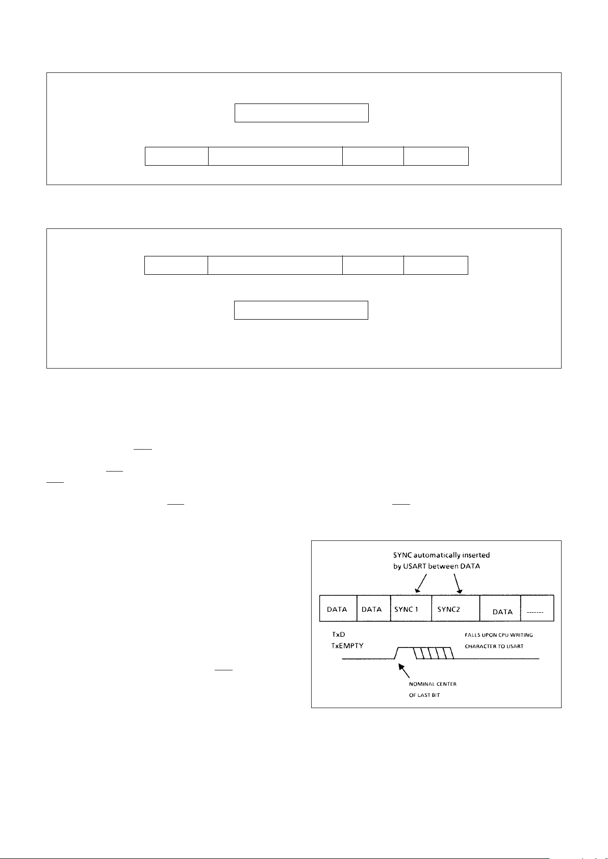
3.6 SYNCHRONOUS MODE (TRANSMISSION)
The TxD output is continuously high until the CPU sends its
first character to the MA28151 which usually is a SYNC
character. When the
CTS line goes low, the first character is
serially transmitted out. All characters are shifted out on the
falling edge of TxC. Data is shifted out at the same rate as the
TxC.
Once transmission has started, the data stream at the TxD
output must continue at the TxC rate. If the CPU does not
provide the MA28151 with a data character before the
MA28151 Transmitter Buffers become empty, the SYNC
characters (or character if in single SYNC character mode) will
be automatically inserted in the TxD data stream. In this case,
the TxEMPTY does not go low when the SYNC is being shifted
out (see figure 8). The TxEMPTY pin is internally reset by a
data character being written into the MA28151.
3.7 SYNCHRONOUS MODE (RECEIVER)
In this mode character synchronisation can be internally or
externally achieved. If the SYNC mode has been
programmed, ENTER-HUNT command should be included in
the first command instruction word written. Data on the RxD
pin is then sampled on the rising edge of
RxC. The content of
the Rx buffer is compared to every bit boundary with the first
SYNC character until a match occurs.
If the MA28151 has been programmed for two SYNC
characters, the subsequent received character is also
compared; when both SYNC characters have been detected,
the USART ends the HUNT mode and is in character
synchronization. The SYNDET pin is then set high, and is reset
automatically by a STATUS READ. If parity is programmed,
SYNDET will not be set until the middle of the parity bit, instead
of the middle of the last data bit.
In the external SYNC mode, synchronization is achieved
by applying a high level on the SYNDET pin, thus forcing the
MA28151 out of the HUNT mode. The high level can be
removed after one
RxC cycle. An ENTER HUNT command
has no effect in the asynchronous mode of operation.
Figure 8: Sync Character Insertion
PARITY BITDATA CHARACTER STOP BITSSTART BIT
DATA CHARACTER
ASSEMBLED SERIAL DATA OUTPUT (TxD)
CPU BYTE (5-8 BITS/CHARACTER)
PARITY BITDATA CHARACTER STOP BITSSTART BIT
DATA CHARACTER
SERIAL DATA INPUT (RxD)
CPU BYTE (5-8 BITS/CHARACTER) (See Note Below)
NOTE: If character length is defined as 5, 6 or 7 bits the unused bits are set to zero.
Page 8

MA28151
8/22
Parity error and overrun error are both checked in the same
way as in the Asynchronous Receive mode. Parity is checked
when not in HUNT, regardless of whether the Receiver is
enabled or not.
The CPU can command the receiver to enter the HUNT
mode if synchronisation is lost. This will also set all the used
character bits in the buffer to a one thus preventing a possible
false SYNDET caused by data that happens to be in the Rx
buffer at ENTER HUNT time.
Note: the SYNDET flip-flop is reset at each Status Read,
regardless of whether internal or external SYNC has been
programmed. This does not cause the MA28151 to return to
the HUNT mode. When in SYNC mode, but not in HUNT, Sync
Detection is still functional, but only occurs at the known word
boundaries. Thus, if one Status Read indicates SYNDET and a
second Status Read also indicates SYNDET, then the
programmed SYNDET characters have been received since
the previous Status Read. (If double character sync has been
contiguously received to gate a SYNDET indication). When
external SYNDET mode is selected, internal Sync Detect is
disabled, and the SYNDET flip-flop may be set at any bit
boundary.
3.9 DATA FORMAT, SYNCHRONOUS MODE
DATA CHARACTERS
ASSEMBLED SERIAL DATA OUTPUT (TxD)
SYNC CHAR 1 SYNC CHAR 2 DATA CHARACTERS
Figure 9: Receive Format, Synchronous Mode
Figure 10: Data Format, Synchronous Mode
DATA CHARACTERS
CPU BYTES (5-8 BITS/CHARACTER)
SYNC CHAR 1 SYNC CHAR 2 DATA CHARACTERS
3.8 MODE INSTRUCTION FORMAT, SYNCHRONOUS MODE
D7D6D5D4D3D2D1D
0
SSES
EP PEN L2 L1 0 0
C
HARACTER LENGTH
5
BITS6BITS7BITS8BITS
0011
0101
PARITY ENABLE AND SENSE
1 = ENABLE 0 = DISABLE
1 = EVEN 0 = ODD
EXTERNAL SYNC DETECT
1 = SYNCDET IS AN INPUT
0 = SYNCDET IS AN OUTPUT
SING
LE CHARACTER SYN
C
1 = SINGLE SYNC CHAR.
0 = DOUBLE SYNC CHAR.
Figure 11: Mode Instruction Format, Synchronous Mode
Page 9

MA28151
9/22
3.10 COMMAND INSTRUCTION DEFINITION
Once the functional definition of the MA28151 has been
programmed by the Mode Instruction and the sync characters
are loaded (if in Sync Mode) then the device is ready to be
used for data communications. The Command Instruction
controls the actual operation of the selected format. Functions
such as: Enable Transmit/Receive, Error Reset and Modem
Controls are provided by the Command Instruction.
Once the Mode Instruction has been written into the
MA28151 and Sync characters inserted, if necessary, then all
further “control writes” (CDN=1) will load a Command
Instruction. A Reset Operation (internal or external) will return
the MA28151 to the Mode instruction format.
Note: Internal Reset on Power-up. When power is first
applied, the MA28151 may come up in the Mode, Sync
character or Command format. To guarantee that the device is
in the Command instruction format before the Reset command
is issued, it is safest to execute the worst-case initialization
sequence (sync mode with two sync characters). Loading
three 00Hs consecutively into the device with CDN=1
configures sync operation and writes two dummy 00H sync
characters. An internal reset command (40H) may then be
issued to return the device to the idle state.
3.11 COMMAND INSTRUCTION FORMAT
D
7
TRANSMIT ENABLE
1 = ENABLE
0 = DISABLE
EH
D
6
IR
D
5
RTS
D
4
ER
D
3
SBRK
D
2
RxE
D
1
DTR
D
0
TxEN
DATA TERMINAL READY
HIGH WILL FORCE DTR
OUTPUT TO ZERO
RECEIVE ENABLE
1 = ENABLE
0 = DISABLE
S
END BREAK CHARACTER
1 = FORCES TxD LOW
0 = NORMAL OPERATION
ERROR RESET
1 = RESET ERROR FLAGS
PE, OE, FE
REQUEST TO SEND
HIGH WILL FORCE RTS
OUTPUT TO ZERO
INTERNAL RESET
HIGH RETURNS THE MA28151 TO
MODE INSTRUCTION FORMAT
ENTER HUNT MODE*
HIGH ENABLES SEARCH FOR SYNC
CHARACTERS (HAS NO EFFECT IN ASYNC MODE)
*NOTE: ERROR RESET must be performed whenever RxENABLE and ENTER-HUNT
are programmed.
Figure 12: Command Instruction Format
Page 10

MA28151
10/22
3.12 STATUS READ DEFINITION
In data communication systems it is often necessary to
examine the status of the active device to ascertain if errors
have occurred or other conditions that require the processor’s
attention. The MA28151 has facilities that allow the
programmer to read the status of the device at any time during
the functional operation. (Status update is inhibited during
status read).
A normal read command is issued by the CPU with CDN
high to accomplish this function.
Some of the bits in the Status Read Format have identical
meanings to external output pins so that the MA28151 can be
used in a completely polled or interrupt-driven environment.
TxRDY is an exception.
Note that status update can have a maximum delay of 28
clock periods from the actual event affecting the status.
3.13 STATUS READ FORMAT
D
7
DSR
D
6
S
YNDET
BRKDET
D
5
FE
D
4
O
E
D
3
PE
D
2
Tx
EMPTY
D
1
RxRDY
D
0
TxRDY
PARITY ERROR
The PE flag is set when the
parity error is detected. It is
reset by the ER bit of the
Command Instruction. PE does
not inhibit the operation of the
MA28151.
Note 1: TxRDY status bit has different meanings from the TxRDY output pin. The former
is not conditioned by CTS and TxEN, the latter is conditioned by both CTS and TxEN.
ie. TxRDY status bit 0 DB buffer empty
TxRDY pin out = DB buffer empty OR (CTSN = 0) OR (TxEN = 1)
Note 1
Same as I/O pins
O
VERRUN ERROR
The OE flag is set when the
CPU does not read a character
before the next one becomes
available. It is reset by the ER
bit of the Command Instruction
OE does not inhibit operation
of the MA28151, however the
previously overrun character is
lost.
FRAMING ERROR (ASYNC
ONLY)
The FE flag is set when a valid
Stop bit is not detected at the
end of every character. It is
reset by the ER bit of the
Command Instruction. FE does
not inhibit the operation of the
MA28151.
DATA SET READY
Indicates that the DSR is at a
zero level.
Figure 13: Status Read Format
Page 11

MA28151
11/22
4. TIMING WAVEFORMS
Figure 14: System Clock Input
Figure 15: Transmitter Clock and Data
Figure 16: Receive Clock and Data
Page 12

MA28151
12/22
Figure 17: Write Data Cycle (CPU to USART)
Figure 19: Write Control or Output Port Cycle (CPU to USART)
Note: tWC includes the response timing of a control byte.
Figure 18: Read Data Cycle (USART to CPU)
Page 13

MA28151
13/22
Figure 20: Read Control or Output Port Cycle (USART to CPU)
Note: tCR includes the effect of CTS on the TxENABLE circuitary.
Figure 21: Transmitter Control and Flag Timing (ASYNC Mode)
Example Format = 7 bit character with parity and 2 stop bits.
Page 14

MA28151
14/22
Figure 22: Receiver Control and Flag Timing (ASYNC Mode)
Example Format = 7 bit character with parity and 2 stop bits.
Page 15

MA28151
15/22
5. AC ELECTRICAL CHARACTERISTICS
Symbol Parameter Min. Max. Units Condition
t
CY
Internal clock cycle time 200 1000 nS Notes 1, 5, 6
t
0
External Clock high pulse width 25 - nS -
t
0
External Clock low pulse width 25 - nS -
tR, t
F
Clock rise and fall time - 10 nS -
t
DTX
TxD delay from falling edge of TxD - 1 µS-
t
TPW
Transmitter input clock pulse width 12xt
CY
- - 1 x baud rate
1xt
CY
- - 16 x and 64 x baud rate
t
TPD
Transmitter input clock pulse delay 15xt
CY
- - 1 x baud rate
3xt
CY
- - 16 x and 64 x baud rate
t
RPW
Receive input clock pulse width 12xt
CY
- - 1 x baud rate
1xt
CY
- - 16 x and 64 x baud rate
t
RPD
Receive input clock pulse delay 15xt
CY
- - 1 x baud rate
3xt
CY
- - 16 x and 64 x baud rate
t
TxRDY
TxRDY pin delay from CENTER of last bit - 8xt
CY
- Note 7
t
TxRDY CLEAR
TxRDY fall from falling DSN (WRITE) - 45 - Note 7
t
RxRDY
RxRDY pin delay from center of last bit - 26xt
CY
- Note 7
t
RxRDY CLEAR
RxRDY fall from falling DSN (READ) - 45 - Note 7
t
TxEMPTY
TxEMPTY from centre of last bit 20xt
CY
- - Note 7
t
WC
Control delay from rising edge of WRITE 8xt
CY
- - Note 7
t
CR
Control to READ set-up time (DSR, CTS) 20xt
CY
- - Note 7
t
AR
Address stable before DSN (CSN, CDN) 0 - ns Note 2
t
RA
Address hold time before DSN (CSN, CDN) 0 - ns Note 2
t
RR
DSN pulse width 20 - ns -
t
RD
Data delay from DSN falling (READ) - 30 ns Note 3
t
DF
DSN rising to data floating (READ) 10 45 ns Note 8
t
DW
Data set-up time to DSN rising (WRITE) 15 - ns -
t
WD
Data hold time to DSN rising (WRITE) 5 - ns -
t
RV
Recovery time between writes (not shown) 6xt
CY
- - Note 4
Notes: 1. AC Timings measured VOH = 1.5 VOL = 1.5.
2. CSN and Command/Data are considered as addresses.
3. Assumes that address is valid before DSN goes low.
4. This recovery time is for Mode Initialisation only. Write data is allowed when TxRDY = 1. Recovery time between
writes for Asynchronous Mode is 8xt
CY
and for Synchronous Mode is 16xtCY.
5. The TxC and RxC frequencies have the following limitation with respect to clock: For 1 x baudrate, fTX or fRX≤1/
(30t
CY
): For 16 x and 64 x baud rate, fTX or fRX ≤1/(4.5tCY).
6. Reset Pulse Width = 6tCY minimum; System clock must be running during Reset.
7. Status update can have a maximum delay of 28 clock periods from the event affecting the status.
8. Data Bus connected to V
DD
via loads of 680Ω (minimum).
Mil-Std-883, method 5005, subgroups 9, 10, 11
Figure 23: AC Electrical Characteristics
Symbol Parameter Min. Max. Units Condition
- Clock Frequency (osc) - 20 MHz -
f
Tx
Transmitter input clock frequency DC 64 kHz 1 x baud rate
DC 310 kHz 16 x baud rate
DC 615 kHz 64 x baud rate
f
Rx
Receiver input clock frequency DC 64 kHz 1x baud rate
DC 310 kHz 16 x baud rate
DC 615 kHz 64 x baud rate
Mil-Std-883, method 5005, subgroups 7, 8A, 8B
Figure 24: Operating AC Electrical Characteristics
Page 16

MA28151
16/22
6. DC CHARACTERISTICS AND RATINGS
Parameter Min Max Units
Supply Voltage -0.5 7 V
Input Voltage -0.3 V
DD
+0.3 V
Current Through Any Pin -20 +20 mA
Operating Temperature -55 125 °C
Storage Temperature -65 150 °C
Note: Stresses above those listed may cause permanent
damage to the device. This is a stress rating only and
functional operation of the device at these conditions, or at
any other condition above those indicated in the operations
section of this specification, is not implied. Exposure to
absolute maximum rating conditions for extended periods
may affect device reliability.
Figure 25: Absolute Maximum Ratings
Total dose radiation not
exceeding 3x10⁵ Rad(SI)
Symbol Parameter Conditions Min Typ Max Units
V
DD
Supply Voltage - 4.5 5.0 5.5 V
V
IH
Input High Voltage - 2.2 - - V
V
IL
Input Low Voltage - - - 0.8 V
V
OH
Output High Voltage IOH = -2mA VDD-0.5 - - V
V
OL
Output Low Voltage IOL = 5mA - - VSS+0.4 V
I
IN
Input Leakage Current (Note 1) VDD = 5.5V, - - ±10 µA
VIN = VSS or V
DD
I
OZ
Tristate Leakage Current (Note 1) VDD = 5.5V, - - ±50 µA
V
IN
= VSS or V
DD
I
DD
Power Supply Current Static, VDD = 5.5V - 0.1 10 mA
VDD = 5V±10%, over full operating temperature range.
Mil-Std-883, method 5005, subgroups 1, 2, 3
Note 1: Guaranteed but not tested at -55°C
Figure 26: Electrical Characteristics
Subgroup Definition
1 Static characteristics specified in Figure 26 at +25°C
2 Static characteristics specified in Figure 26 at +125°C
3 Static characteristics specified in Figure 26 at -55°C
7 Functional characteristics specified in Figure 24 at +25°C
8A Functional characteristics specified in Figure 24 at +125°C
8B Functional characteristics specified in Figure 24 at -55°C
9 Switching characteristics specified in Figure 23 at +25°C
10 Switching characteristics specified in Figure 23 at +125°C
11 Switching characteristics specified in Figure 23 at -55°C
Figure 27: Definition of Mil-Std-883, Method 5005 Subgroups
Page 17

MA28151
17/22
7. OUTLINES AND PIN ASSIGNMENTS
D
W
A
e b Z
H
A
1
15°
M
E
C
e
1
Seating Plane
114
2815
Ref
Millimetres Inches
Min. Nom. Max. Min. Nom. Max.
A - - 5.715 - - 0.225
A1 0.38 - 1.53 0.015 - 0.060
b 0.35 - 0.59 0.014 - 0.023
c 0.20 - 0.36 0.008 - 0.014
D - - 36.02 - - 1.418
e - 2.54 Typ. - - 0.100 Typ. -
e1 - 15.24 Typ. - - 0.600 Typ. -
H 4.71 - 5.38 0.185 - 0.212
Me - - 15.90 - - 0.626
Z - - 1.27 - - 0.050
W - - 1.53 - - 0.060
XG404
28
D1
27
D0
26
Vdd
25
RxC
24
DTR
23
RTS
22
DSR
21
RESET
20
CLK
19
TxD
18
TxE
17
CTS
16
SYNDET
15
TxRDY
1
D2
2
D3
3
RxD
4
GND
5
D4
6
D5
7
D6
8
D7
9
TxC
10
RDWN
11
CSN
12
CDN
13
DSN
14
RxRD
Y
Top
View
Figure 28: 28-Lead Ceramic DIL (Solder Seal) - Package Style C
Page 18

MA28151
18/22
Figure 29: 48-Pad Leadless Chip Carrier - Package Style L
Bottom
View
Pad 1
Radius r
3 corners
E
Z
e b
1
D A
Ref
Millimetres Inches
Min. Nom. Max. Min. Nom. Max.
A - - 2.29 - - 0.090
b1 - 0.51 - - 0.020 -
D - - 14.60 - - 0.575
E - - 14.60 - - 0.575
e - 1.02 - - 0.040 Z - 1.52 Typ. - - 0.060 Typ. -
XG431
Bottom
View
19
181716151413121110987
20
21
22
23
24
25
26
27
28
29
30
313233343536373839404142
6
5
4
3
2
1
48
47
46
45
44
43
N
C
C
DN
D
S
N
RxRDY
N
CNC
TxRDY
S
YNDET
N
C
CTS
TxEMPTY
N
CNC
G
ND
RxD
D3
N
C
D2
N
CNC
D1
D0
N
C
Vdd
NCD4D5
NC
D6
NC
D7
NC
TxC
RDW
N
CSN
NC
NC
RxC
NC
DTR
RTS
NC
DSR
NC
RESET
CLK
TxD
NC
Page 19

MA28151
19/22
Top View
j1
D1L
Pin 1
j2
b
e
D2
Z
A1
A
c
Ref
Millimetres Inches
Min. Nom. Max. Min. Nom. Max.
A - - 2.72 - - 0.107
A1 1.83 - 2.24 0.072 - 0.088
b 0.41 - 0.51 0.016 - 0.020
c 0.20 - 0.30 0.008 - 0.012
D1, D2 23.88 - 24.51 0.940 - 0.960
e - 2.54 - - 0.050 j1 - 1.02 - - 0.040 j2 - 0.51 - - 0.020 L 10.16 - 10.54 0.400 - 0.415
Z 1.65 - 2.16 0.065 - 0.085
XG540
Figure 30a: 68-Lead Topbraze Flatpack - Package Style F
Page 20

MA28151
20/22
Figure 30b: 68-Lead Topbraze Flatpack - Package Style F
Top View
27
26 25 24 23 22 21 20 19 18 17 16 15 14 13 12 11
28
29
30
31
32
33
34
35
36
37
38
39
40
41
42
43
44 45 46 47 48 49 50 51 52 53 54 55 56 57 58 59
NC
NC
CDN
NC
DSN
NC
RXRDY
NC
TXRD
Y
NC
SYNDET
NC
CTS
NC
TXE
NC
NC
NC
NC
CSNNCRDWN
NC
TXC
NC
D7
NC
D6
NC
D5
NCD4NC
NC
NC
TXD
NC
CLK
NC
ESET
NC
DSR
NC
RTS
NC
DTR
NC
RXC
NC
Page 21

MA28151
21/22
8. RADIATION TOLERANCE
Total Dose Radiation Testing
For product procured to guaranteed total dose radiation
levels, each wafer lot will be approved when all sample
devices from each lot pass the total dose radiation test.
The sample devices will be subjected to the total dose
radiation level (Cobalt-60 Source), defined by the ordering
code, and must continue to meet the electrical parameters
specified in the data sheet. Electrical tests, pre and post
irradiation, will be read and recorded.
Dynex Semiconductor can provide radiation testing
compliant with MIL-STD-883 Ionizing Radiation (Total Dose)
test 1019.
9. ORDERING INFORMATION
For details of reliability, QA/QC, test and assembly
options, see ‘Manufacturing Capability and Quality
Assurance Standards’ Section 9.
Unique Circuit Designator
S
R
Q
H
Radiation Hard Processing
100 kRads (Si) Guaranteed
300 kRads (Si) Guaranteed
1000 kRads (Si) Guaranteed
Radiation Tolerance
C
F
L
Ceramic DIL (Solder Seal)
Flatpack (Solder Seal)
Leadless Chip Carrier
Package Type
QA/QCI Process
(See Section 9 Part 4)
Test Process
(See Section 9 Part 3)
Assembly Process
(See Section 9 Part 2)
L
C
D
E
B
S
Rel 0
Rel 1
Rel 2
Rel 3/4/5/STACK
Class B
Class S
Reliability Level
MAx28151xxxxx
Total Dose (Function to specification)* 3x10⁵ Rad(Si)
Transient Upset (Stored data loss) 5x10
10
Rad(Si)/sec
Transient Upset (Survivability) >1x10¹² Rad(Si)/sec
Neutron Hardness (Function to specification) >1x10¹⁵ n/cm
2
Single Event Upset** <1x10
-10
Errors/bit day
Latch Up Not possible
* Other total dose radiation levels available on request
** Worst case galactic cosmic ray upset - interplanetary/high altitude orbit
Figure 31: Radiation Hardness Parameters
Page 22

MA28151
22/22
CUSTOMER SERVICE CENTRES
France, Benelux, Italy and Spain Tel: +33 (0)1 69 18 90 00. Fax: +33 (0)1 64 46 54 50
North America Tel: 011-800-5554-5554. Fax: 011-800-5444-5444
UK, Germany, Scandinavia & Rest Of World Tel: +44 (0)1522 500500. Fax: +44 (0)1522 500020
SALES OFFICES
France, Benelux, Italy and Spain Tel: +33 (0)1 69 18 90 00. Fax: +33 (0)1 64 46 54 50
Germany Tel: 07351 827723
North America Tel: (613) 723-7035. Fax: (613) 723-1518. Toll Free: 1.888.33.DYNEX (39639) /
Tel: (831) 440-1988. Fax: (831) 440-1989 / Tel: (949) 733-3005. Fax: (949) 733-2986.
UK, Germany, Scandinavia & Rest Of World Tel: +44 (0)1522 500500. Fax: +44 (0)1522 500020
These offices are supported by Representatives and Distributors in many countries world-wide.
© Dynex Semiconductor 2000 Publication No. DS3574-5 Issue No. 5.0 January 2000
TECHNICAL DOCUMENTATION – NOT FOR RESALE. PRINTED IN UNITED KINGDOM
HEADQUARTERS OPERATIONS
DYNEX SEMICONDUCTOR LTD
Doddington Road, Lincoln.
Lincolnshire. LN6 3LF. United Kingdom.
Tel: 00-44-(0)1522-500500
Fax: 00-44-(0)1522-500550
DYNEX POWER INC.
Unit 7 - 58 Antares Drive,
Nepean, Ontario, Canada K2E 7W6.
Tel: 613.723.7035
Fax: 613.723.1518
Toll Free: 1.888.33.DYNEX (39639)
This publication is issued to provide information only which (unless agreed by the Company in writing) may not be used, applied or reproduced for any purpose nor form part of any order or contract nor to be regarded
as a representation relating to the products or services concerned. No warranty or guarantee express or implied is made regarding the capability, performance or suitability of any product or service. The Company
reserves the right to alter without prior notice the specification, design or price of any product or service. Information concerning possible methods of use is provided as a guide only and does not constitute any
guarantee that such methods of use will be satisfactory in a specific piece of equipment. It is the user's responsibility to fully determine the performance and suitability of any equipment using such information and
to ensure that any publication or data used is up to date and has not been superseded. These products are not suitable for use in any medical products whose failure to perform may result in significant injury
or death to the user. All products and materials are sold and services provided subject to the Company's conditions of sale, which are available on request.
All brand names and product names used in this publication are trademarks, registered trademarks or trade names of their respective owners.
http://www.dynexsemi.com
e-mail: power_solutions@dynexsemi.com
Datasheet Annotations:
Dynex Semiconductor annotate datasheets in the top right hard corner of the front page, to indicate product status. The annotations are as follows:-
Target Information: This is the most tentative form of information and represents a very preliminary specification. No actual design work on the product has been started.
Preliminary Information: The product is in design and development. The datasheet represents the product as it is understood but details may change.
Advance Information: The product design is complete and final characterisation for volume production is well in hand.
No Annotation: The product parameters are fixed and the product is available to datasheet specification.
 Loading...