

Datasheet MACH435Q-25JC, MACH435Q-20JC, MACH435-20JC, MACH435-15JC, MACH435-12JC Datasheet (Lattice Semiconductor Corporation)
Page 1

FINAL
COM’L: -12/15/20, Q-20/25
MACH435-12/15/20, Q-20/25
High-Density EE CMOS Programmable Logic
DISTINCTIVE CHARACTERISTICS
■ 84 Pins in PLCC
■ 128 Macrocells
■ 12 ns tPD
■ 83.3 MHz fCNT
■ 70 Inputs with pull-up resistors
■ 64 Outputs
■ 192 Flip-flops
— 128 Macrocell flip-flops
— 64 Input flip-flops
■ Up to 20 product terms per function, with XOR
GENERAL DESCRIPTION
The MACH435 is a member of our high-performance
EE CMOS MACH 4 family. This device has approximately twelve times the macrocell capability of the
popular PAL22V10, with significant density and functional features that the PAL22V10 does not provide.
The MACH435 consists of eight PAL blocks interconnected by a programmable central switch matrix. The
central switch matrix connects the PAL blocks to each
other and to all input pins, providing a high degree of
connectivity between the fully-connected PAL blocks.
This allows designs to be placed and routed efficiently.
Routability is further enhanced by an input switch matrix
and an output switch matrix. The input switch matrix
provides input signals with alternative paths into the
central switch matrix; the output switch matrix provides
flexibility in assigning macrocells to I/O pins.
The MACH435 has macrocells that can be configured
as synchronous or asynchronous. This allows designers
to implement both synchronous and asynchronous logic
■ Flexible clocking
— Four global clock pins with selectable edges
— Asynchronous mode available for each
macrocell
■ 8 “PAL33V16” blocks
■ Input and output switch matrices for high
routability
■ Fixed, predictable, deterministic delays
■ Pin compatible with MACH130, MACH131,
MACH230, and MACH231
together on the same device. The two types of design
can be mixed in any proportion, since the selection on
each macrocell affects only that macrocell.
Up to 20 product terms per function can be assigned. It
is possible to allocate some product terms away from a
macrocell without losing the use of that macrocell for
logic generation.
The MACH435 macrocell provides either registered or
combinatorial outputs with programmable polarity. If a
registered configuration is chosen, the register can be
configured as D-type, T-type, J-K, or S-R to help reduce
the number of product terms used. The flip-flop can also
be configured as a latch. The register type decision can
be made by the designer or by the software.
All macrocells can be connected to an I/O cell through
the output switch matrix. The output switch matrix
makes it possible to make significant design changes
while minimizing the risk of pinout changes.
Lattice Semiconductor
Publication# 17469 Rev. E Amendment/0
Issue Date: May 1995
Page 2
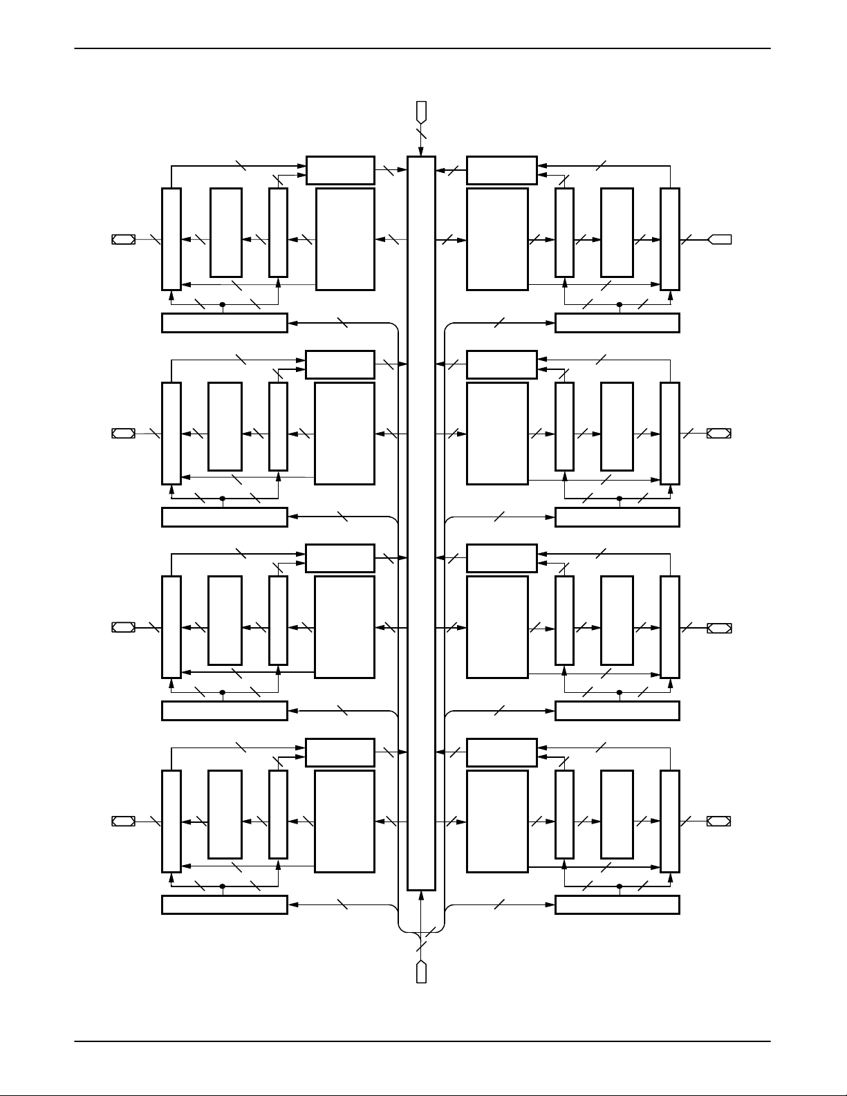
BLOCK DIAGRAM
I2, I5
2
8
8
I/O Cells
I/O Cells
16
Matrix
8
Output Switch
8
4
Clock Generator
16
Matrix
8
Output Switch
8
4
Clock Generator
16
16
16
4
16
16
4
16
Input Switch
16
Macrocells
OE
Input Switch
16
Macrocells
OE
Input Switch
Matrix
66 X 90
AND Logic Array
and Logic Allocator
4
Matrix
66 X 90
AND Logic Array
and Logic Allocator
4
Matrix
24
33
24
33
24
33
33
Central Switch Matrix
Input Switch
Matrix
24
66 X 90
Input Switch
Matrix
24
66 X 90
Input Switch
Matrix
24
16
AND Logic Array
and Logic Allocator
OE
4
16
AND Logic Array
and Logic Allocator
OE
4
16
16
16
Macrocells
8
4
Clock Generator
16
16
16
Macrocells
8
4
Clock Generator
16
16
Matrix
8
Output Switch
4
Matrix
8
Output Switch
4
8
I/O Cells
8
I/O Cells
I/O32–I/O39I/O40–I/O47I/O48–I/O55I/O56–I/O63
I/O0–I/O7 I/O8–I/O15 I/O16–I/O23 I/O24–I/031
8
8
8
I/O Cells
4
Clock Generator
8
I/O Cells
4
Clock Generator
Matrix
16
Output Switch
8
4
16
16
Matrix
16
Output Switch
8
4
16
Macrocells
OE
Input Switch
16
Macrocells
OE
66 X 90
AND Logic Array
and Logic Allocator
4
Matrix
66 X 90
AND Logic Array
and Logic Allocator
4
33
24
33
4
4
CLK0/I0, CLK1/I1,
CLK2/I3, CLK3/I4
33
Input Switch
24
33
66 X 90
AND Logic Array
and Logic Allocator
OE
4
Matrix
66 X 90
AND Logic Array
and Logic Allocator
OE
4
16
16
16
Macrocells
4
Clock Generator
16
16
16
Macrocells
4
Clock Generator
Matrix
8
Output Switch
8
4
Matrix
8
Output Switch
8
4
8
I/O Cells
8
I/O Cells
17469E-1
2 MACH435-12/15/20, Q-20/25
Page 3
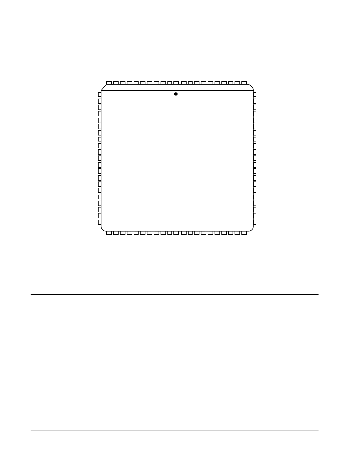
CONNECTION DIAGRAM
Top View
CC
11
12
13
14
15
16
17
18
19
20
21
22
23
24
25
26
27
28
29
30
31
32
33
I/O10
I/O11
I/O12
I/O13
I/O14
I/O15
CLK
CLK
I/O16
I/O17
I/O18
I/O19
I/O20
I/O21
I/O22
I/O23
I/O8
I/O9
0/I0
V
GND
1/I1
GND
GND
10
34
I/O7
9
35
I/O6
8
36
I/O5
7
37
I/O4
6
38
I/O3
5
39
I/O2
4
40
I/O1
3
41
PLCC
CC
V
GND
I/O0
2
1
42
43
84
44
V
CC
83
45
I
5
82
46
I/O62
I/O63
81
47
I/O61
80
48
79
49
I/O60
I/O59
78
50
I/O58
77
51
I/O57
76
52
75
53
I/O56
74
73
72
71
70
69
68
67
66
65
64
63
62
61
60
59
58
57
56
55
54
GND
I/O55
I/O54
I/O53
I/O52
I/O51
I/O50
I/O49
I/O48
CLK
3/I4
GND
V
CC
CLK2/I
I/O47
I/O46
I/O45
I/O44
I/O43
I/O42
I/O41
I/O40
3
Note:
Pin-compatible with MACH130, MACH131, MACH230, and MACH231
PIN DESIGNATIONS
CLK/I = Clock or Input
GND = Ground
I = Input
I/O = Input/Output
VCC = Supply Voltage
I/O24
I/O25
I/O26
I/O27
I/O28
I/O29
I/O30
I/O31
2
I
CC
CC
V
V
GND
I/O33
I/O32
I/O34
I/O35
I/O36
I/O37
I/O39
I/O38
GND
17469E-2
3MACH435-12/15/20, Q-20/25
Page 4
ORDERING INFORMATION
Commercial Products
Programmable logic products for commercial applications are available with several ordering options. The order number
(Valid Combination) is formed by a combination of:
MACH -12 J C
FAMILY TYPE
MACH = Macro Array CMOS High-Speed
DEVICE NUMBER
435 = 2nd Generation, 128 Macrocells, 84 Pins
435Q = 2nd Generation, 128 Macrocells, 84 Pins,
SPEED
-12 = 12 ns t
-15 = 15 ns t
-20 = 20 ns t
-25 = 25 ns t
Quarter Power
PD
PD
PD
PD
Valid Combinations
MACH435-12
MACH435-15
MACH435-20
MACH435Q-20
MACH435Q-25
JC
435
OPTIONAL PROCESSING
Blank = Standard Processing
OPERATING CONDITIONS
C = Commercial (0
PACKAGE TYPE
J = 84-Pin Plastic Leaded
Chip Carrier (PL 084)
Valid Combinations
The Valid Combinations table lists configurations
planned to be supported in volume for this device.
Consult your local sales office to confirm availability of specific valid combinations and to check on newly
released combinations.
°C to +70°C)
4 MACH435-12/15/20, Q-20/25
Page 5

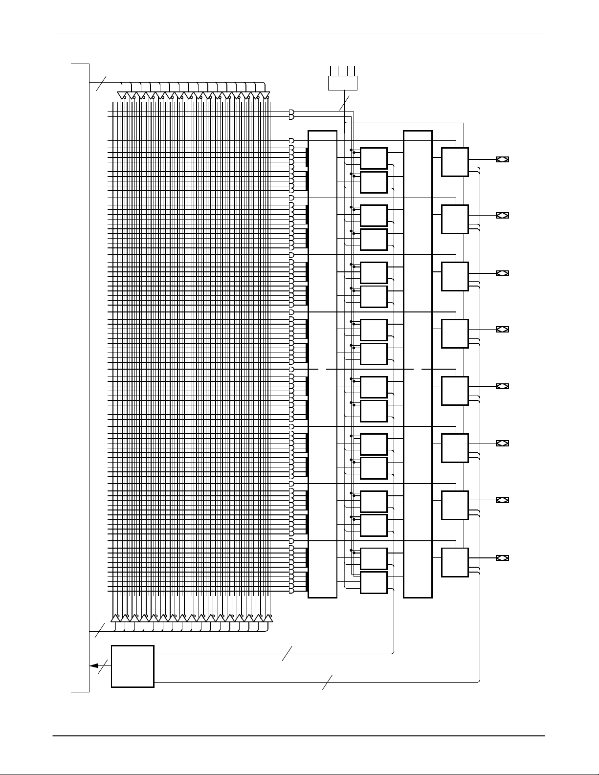
FUNCTIONAL DESCRIPTION
The MACH435 consists of eight PAL blocks connected
by a central switch matrix. There are 64 I/O pins and 6
dedicated input pins feeding the central switch matrix.
These signals are distributed to the eight PAL blocks for
efficient design implementation. There are 4 global
clock pins that can also be used as dedicated inputs.
All inputs and I/O pins have built-in pull-up resistors.
While it is always good design practice to tie unused
pins high, the pull-up resistors provide design security
and stability in the event that unused pins are left
disconnected.
The PAL Blocks
Each PAL block in the MACH435 (Figure 1) contains a
clock generator, a 90-product-term logic array, a logic
allocator, 16 macrocells, an output switch matrix, 8 I/O
cells, and an input switch matrix. The central switch
matrix feeds each PAL block with 33 inputs. This makes
the PAL block look effectively like an independent
“PAL33V16” with 8 to 16 buried macrocells.
In addition to the logic product terms, individual output
enable product terms and two PAL block initialization
product term are provided. Each I/O pin can be
individually enabled. All flip-flops that are in the
synchronous mode within a PAL block are initialized
together by either of the PAL block initialization product
terms.
The Central Switch Matrix and Input
Switch Matrix
The MACH435 central switch matrix is fed by the input
switch matrices in each PAL block. Each PAL block
provides 16 internal feedback signals, 8 registered input
signals, and 8 I/O pin signals to the input switch matrix.
Of these 32 signals, 24 decoded signals are provided to
the central switch matrix by the input switch matrix. The
central switch matrix distributes these signals back to
the PAL blocks in a very efficient manner that provides
for high performance. The design software automatically configures the input and central switch matrices
when fitting a design into the device.
The Product-Term Array
The MACH435 product-term array consists of 80
product terms for logic use, eight product terms for
output enable use, and two product terms for global PAL
block initialization. Each macrocell has a nominal
allocation of 5 product terms for logic, although the logic
allocator allows for logic redistribution. Each I/O pin has
its own individual output enable term. The initialization
product terms provide asynchronous reset or preset to
synchronous-mode macrocells in the PAL block.
The Logic Allocator
The logic allocator in the MACH435 takes the 80 logic
product terms and allocates them to the 16 macrocells
as needed. Each macrocell can be driven by up to 20
product terms if in synchronous mode, or 18 product
terms if in asynchronous mode. When product terms are
routed away from a macrocell, it is possible to route all 5
product terms away, which precludes the use of the
macrocell for logic generation; or it is possible to route
only 4 product terms away, leaving one for simple
function generation. The design software automatically
configures the logic allocator when fitting the design into
the device.
The logic allocator also provides an exclusive-OR gate.
This gate allows generation of combinatorial exclusiveOR logic, such as comparison or addition. It allows
registered exclusive-OR functions, such as CRC generation, to be implemented more efficiently. It also
makes in possible to emulate all flip-flop types with a
D-type flip-flop. Register type emulation is automatically
handled by the design software.
Table 1 illustrates which product term clusters are
available to each macrocell within a PAL block. Refer to
Figure 1 for cluster and macrocell numbers.
The Clock Generator
Each PAL block has a clock generator that can generate
four clock signals for use throughout the PAL block.
These four signals are available to all macrocells and
I/O cells in the PAL block, whether in synchronous or
asynchronous mode. The clock generator chooses the
four signals from the eight possible signals given by the
true and complement versions of the four global clock
pin signals.
5MACH435-12/15/20, Q-20/25
Page 6
Table 1. Logic Allocation
Macrocell Available Clusters
M0 C0, C1, C2
M1 C0, C1, C2, C3
M2 C1, C2, C3, C4
M3 C2, C3, C4, C5
M4 C3, C4, C5, C6
M5 C4, C5, C6, C7
M6 C5, C6, C7, C8
M7 C6, C7, C8, C9
M8 C7, C8, C9, C10
M9 C8, C9, C10, C11
M10 C9, C10, C11, C12
M11 C10, C11, C12, C13
M12 C11, C12, C13, C14
M13 C12, C13, C14, C15
M14 C13, C14, C15
M15 C14, C15
The Macrocell and Output Switch Matrix
The MACH435 has 16 macrocells, half of which can
drive I/O pins; this selection is made by the output switch
matrix. Each macrocell can drive one of four I/O cells.
The allowed combinations are shown in Table 2. Please
refer to Figure 1 for macrocell and I/O pin numbers.
Table 2. Output Switch Matrix Combinations
Macrocell Routable to I/O Pins
M0, M1 I/O5, I/O6, I/O7, I/O0
M2, M3 I/O6, I/O7, I/O0, I/O1
M4, M5 I/O7, I/O0, I/O1, I/O2
M6, M7 I/O0, I/O1, I/O2, I/O3
M8, M9 I/O1, I/O2, I/O3, I/O4
M10, M11 I/O2, I/O3, I/O4, I/O5
M12, M13 I/O3, I/O4, I/O5, I/O6
M14, M15 I/O4, I/O5, I/O6, I/O7
I/O Pin Available Macrocells
I/O0 M0, M1, M2, M3, M4, M5, M6, M7
I/O1 M2, M3, M4, M5, M6, M7, M8, M9
I/O2 M4, M5, M6, M7, M8, M9, M10, M11
I/O3 M6, M7, M8, M9, M10, M11, M12, M13
I/O4 M8, M9, M10, M11, M12, M13, M14, M15
I/O5 M10, M11, M12, M13, M14, M15, M0, M1
I/O6 M12, M13, M14, M15, M0, M1, M2, M3
I/O7 M14, M15, M0, M1, M2, M3, M4, M5
The macrocells can be configured as registered,
latched, or combinatorial. In combination with the logic
allocator, the registered configuration can be any of the
standard flip-flop types. The macrocell provides internal
feedback whether configured with or without the flipflop, and whether or not the macrocell drives an I/O cell.
The flip-flop clock depends on the mode selected for
the macrocell. In synchronous mode, any of the PAL
block clocks generated by the Clock Generator can be
used. In asynchronous mode, the additional choice of
either edge of an individual product-term clock is
available.
Initialization can be handled as part of a bank of
macrocells via the PAL block initialization terms if in
synchronous mode, or individually if in asynchronous
mode. In synchronous mode, one of the PAL block
product terms is available each for preset and reset. The
swap function determines which product term drives
which function. This allows initialization polarity compatibility with the MACH 1 and 2 series. In asynchronous
mode, one product term can be used either to drive reset
or preset.
The I/O Cell
The I/O cell in the MACH435 consists of a three-state
buffer and an input flip-flop. The I/O cell is driven by one
of the macrocells, as selected by the output switch
matrix. Each I/O cell can take its input from one of eight
macrocells. The three-state buffer is controlled by an
individual product term. The input flip-flop can be
configured as a register or latch. Both the direct I/O
signal and the registered/latched signal are available to
the input switch matrix, and can be used simultaneously
if desired.
6 MACH435-12/15/20, Q-20/25
Page 7
16
CLK0/I0
CLK1/I1
Clock
Generator
4
CLK2/I3
CLK3/I4
Central Switch Matrix
C0
M0
C1
M1
C2
M2
C3
M3
C4
M4
C5
M5
C6
M6
C7
M7
C8
M8
Logic Allocator
C9
M9
Macrocell
Macrocell
Macrocell
Macrocell
Macrocell
Macrocell
Macrocell
Macrocell
Macrocell
Macrocell
M0
M1
M2
M3
M4
M5
M6
M7
M8
Output Switch Matrix
M9
I/O
O0
Cell
I/O
O1
Cell
I/O
O2
Cell
I/O
O3
Cell
I/O
O4
Cell
I/O0
I/O1
I/O2
I/O3
I/O4
17
24
Input
Switch
Matrix
C10
M10
C11
M11
C12
M12
C13
M13
C14
M14
C15
M15
16
16
Figure 1. MACH435 PAL Block
Macrocell
Macrocell
Macrocell
Macrocell
Macrocell
Macrocell
M10
M11
M12
M13
M14
M15
I/O
O5
Cell
I/O
O6
Cell
I/O
O7
Cell
I/O5
I/O6
I/O7
17469E-3
7MACH435-12/15/20, Q-20/25
Page 8
ABSOLUTE MAXIMUM RATINGS
Storage Temperature –65°C to +150°C. . . . . . . . . . .
Ambient Temperature
with Power Applied –55°C to +125°C. . . . . . . . . . . . .
Supply Voltage with
Respect to Ground –0.5 V to +7.0 V. . . . . . . . . . . . .
DC Input Voltage –0.5 V to V
DC Output or
CC
+0.5 V. . . . . . . . . . . .
OPERATING RANGES
Commercial (C) Devices
Temperature (T
in Free Air 0°C to +70°C. . . . . . . . . . . . . . . . . . . . . . .
Supply Voltage (V
Respect to Ground +4.75 V to +5.25 V. . . . . . . . . . . .
Operating ranges define those limits between which the
functionality of the device is guaranteed.
) Operating
A
) with
CC
I/O Pin Voltage –0.5 V to VCC +0.5 V. . . . . . . . . . . . .
Static Discharge Voltage 2001 V. . . . . . . . . . . . . . . . .
Latchup Current
(T
= 0°C to +70°C) 200 mA. . . . . . . . . . . . . . . . . . . .
A
Stresses above those listed under Absolute Maximum
Ratings may cause permanent device failure. Functionality at
or above these limits is not implied. Exposure to Absolute
Maximum Ratings for extended periods may affect device
reliability. Programming conditions may differ.
DC CHARACTERISTICS over COMMERCIAL operating ranges unless otherwise specified
Parameter
Symbol Parameter Description Test Conditions Min Typ Max Unit
V
OH Output HIGH Voltage IOH = –3.2 mA, VCC = Min 2.4 V
IN = VIH or VIL
V
V
V
V
I
I
I
OZH
I
OZL
I
I
OL
IH
IL
IH
IL
SC
CC
Output LOW Voltage IOL = 24 mA, VCC = Min 0.5 V
V
= VIH or V
IN
(Note 1)
IL
Input HIGH Voltage Guaranteed Input Logical HIGH 2.0 V
Voltage for all Inputs (Note 2)
Input LOW Voltage Guaranteed Input Logical LOW 0.8 V
Voltage for all Inputs (Note 2)
Input HIGH Leakage Current VIN = 5.25 V, VCC = Max (Note 3) 10 µA
Input LOW Leakage Current VIN = 0 V, V
Off-State Output Leakage V
= 5.25 V, VCC = Max
OUT
Current HIGH VIN = V
Off-State Output Leakage V
Current LOW V
Output Short-Circuit Current V
Supply Current (Typical) V
= 0 V, VCC = Max
OUT
= V
IN
= 0.5 V, VCC = Max (Note 4) –30 –160 mA
OUT
= 0 V, Outputs Open (I
IN
V
= 5.0 V, f =25 MHz, TA = 25°C (Note 5)
CC
= Max (Note 3) –100 µA
CC
or VIL (Note 3)
IH
or VIL (Note 3)
IH
= 0 mA) 255 mA
OUT
10
–100
µA
µA
CAPACITANCE (Note 6)
Parameter
Symbol Parameter Description Test Conditions Typ Unit
C
IN
C
OUT
Input Capacitance V
Output Capacitance V
Notes:
1. Total I
for one PAL block should not exceed 128 mA.
OL
2. These are absolute values with respect to device ground and all overshoots due to system or tester noise are included.
3. I/O pin leakage is the worst case of I
and I
IL
(or IIH and I
OZL
4. Not more than one output should be shorted at a time and duration of the short-circuit should not exceed one second.
= 0.5 V has been chosen to avoid test problems caused by tester ground degradation.
V
OUT
5. Measured with a 16-bit up/down counter pattern. This pattern is programmed in each PAL block and capable of being loaded,
enabled, and reset.
6. These parameters are not 100% tested, but are evaluated at initial characterization and at any time the design is modified
where capacitance may be affected.
8 MACH435-12 (Com’l)
= 2.0 V VCC = 5.0 V, TA = 25°C, 6 pF
IN
= 2.0 V f = 1 MHz 8 pF
OUT
).
OZH
Page 9
SWITCHING CHARACTERISTICS over COMMERCIAL operating ranges (Note 1)
Parameter
-12
Symbol Parameter Description Min Max Unit
t
t
t
t
COA
t
WLA
t
WHA
f
MAXA
t
t
t
COS
t
WLS
t
WHS
f
MAXS
t
PD
SA
HA
SS
HS
SLA
Input, I/O, or Feedback to Combinatorial Output 3 12 ns
Setup Time from Input, I/O, or D-type 5 ns
Feedback to Product Term Clock
T-type 6 ns
Register Data Hold Time Using Product Term Clock 5 ns
Product Term Clock to Output 4 14 ns
Product Term, Clock Width
LOW 8 ns
HIGH 8 ns
External Feedback
Maximum Frequency
D-type 58.8 MHz
Using Product Term
Clock (Note 2)
Internal Feedback (f
CNTA
)
No Feedback (Note 3)
Setup Time from Input, I/O, or Feedback
to Global Clock
D-type 52.6 MHz
T-type 50 MHz
T-type 55.6 MHz
62.5 MHz
D-type 7 ns
T-type 8 ns
Register Data Hold Time Using Global Clock 0 ns
Global Clock to Output 2 8 ns
Global Clock Width
LOW 6 ns
HIGH 6 ns
D-type 66.7 MHz
Maximum Frequency
D-type 83.3 MHz
Using Global
Clock (Note 2)
83.3 MHz
External Feedback
Internal Feedback (f
No Feedback (Note 3)
CNTA
T-type 62.5 MHz
)
T-type 76.9 MHz
Setup Time from Input, I/O, or Feedback to 5 ns
Product Term Clock
t
t
t
HLA
GOA
GWA
Latch Data Hold Time Using Product Term Clock 5 ns
Product Term Gate to Output 16 ns
Product Term Gate Width LOW (for LOW transparent) 6 ns
or HIGH (for HIGH transparent)
t
t
t
t
SLS
HLS
GOS
GWS
Setup Time from Input, I/O, or Feedback to Global Gate 8 ns
Latch Data Hold Time Using Global Gate 0 ns
Gate to Output 10 ns
Global Gate Width LOW (for LOW transparent) 6 ns
or HIGH (for HIGH transparent)
t
PDL
Input, I/O, or Feedback to Output Through
Transparent Input or Output Latch 14 ns
t
t
t
SIR
HIR
ICO
Input Register Setup Time 2 ns
Input Register Hold Time 3 ns
Input Register Clock to Combinatorial Output 18 ns
9MACH435-12 (Com’l)
Page 10

SWITCHING CHARACTERISTICS over COMMERCIAL operating ranges (Note 1)
(continued)
Parameter
Symbol Parameter Description Min Max Unit
t
ICS
Input Register Clock to Output Register Setup D-type 9 ns
T-type 10 ns
t
WICL
t
WICH
f
MAXIR
t
SIL
t
HIL
t
IGO
t
IGOL
Input Register Clock Width
Maximum Input Register Frequency 83.3 MHz
Input Latch Setup Time 2 ns
Input Latch Hold Time 3 ns
Input Latch Gate to Combinatorial Output 16 ns
Input Latch Gate to Output Through Transparent
LOW 6 ns
HIGH 6 ns
Output Latch 18 ns
Setup Time from Input, I/O, or Feedback Through
t
SLLA
Transparent Input Latch to Product Term Output 4 ns
Latch Gate
t
IGSA
Input Latch Gate to Output Latch Setup Using 4 ns
Product Term Output Latch Gate
t
SLLS
Setup Time from Input, I/O, or Feedback Through
Transparent Input Latch to Global Output Latch Gate 9 ns
t
IGSS
Input Latch Gate to Output Latch Setup Using Global 9 ns
Output Latch Gate
t
WIGL
t
PDLL
Input Latch Gate Width LOW 6 ns
Input, I/O, or Feedback to Output Through Transparent
Input and Output Latches 16 ns
t
t
ARW
t
ARR
t
t
APW
t
APR
t
t
AR
AP
EA
ER
Asynchronous Reset to Registered or Latched Output 16 ns
Asynchronous Reset Width (Note 1) 12 ns
Asynchronous Reset Recovery Time (Note 1) 10 ns
Asynchronous Preset to Registered or Latched Output 16 ns
Asynchronous Preset Width (Note 1) 12 ns
Asynchronous Preset Recovery Time (Note 1) 8 ns
Input, I/O, or Feedback to Output Enable 2 12 ns
Input, I/O, or Feedback to Output Disable 2 12 ns
-12
Notes:
1. See Switching Test Circuit at the end of this Data Book for test conditions.
2. These parameters are not 100% tested, but are evaluated at initial characterization and at any time the design is modified
where frequency may be affected.
3. This parameter does not apply to flip-flops in the emulated mode since the feedback path is required for emulation.
10 MACH435-12 (Com’l)
Page 11

ABSOLUTE MAXIMUM RATINGS
Storage Temperature –65°C to +150°C. . . . . . . . . . .
Ambient Temperature
with Power Applied –55°C to +125°C. . . . . . . . . . . . .
OPERATING RANGES
Commercial (C) Devices
Temperature (T
in Free Air 0°C to +70°C. . . . . . . . . . . . . . . . . . . . . . .
) Operating
A
Supply Voltage with
Respect to Ground –0.5 V to +7.0 V. . . . . . . . . . . . .
DC Input Voltage –0.5 V to VCC +0.5 V. . . . . . . . . . . .
DC Output or
I/O Pin Voltage –0.5 V to VCC +0.5 V. . . . . . . . . . . . .
Supply Voltage (V
Respect to Ground +4.75 V to +5.25 V. . . . . . . . . . . .
Operating ranges define those limits between which the functionality of the device is guaranteed.
CC
) with
Static Discharge Voltage 2001 V. . . . . . . . . . . . . . . . .
Latchup Current (T
Stresses above those listed under Absolute Maximum Ratings
may cause permanent device failure. Functionality at or above
these limits is not implied. Exposure to Absolute Maximum
Ratings for extended periods may affect device reliability.
Programming conditions may differ.
= 0°C to +70°C) 200 mA. . . . . .
A
DC CHARACTERISTICS over COMMERCIAL operating ranges unless otherwise specified
Parameter
Symbol Parameter Description Test Conditions Min Typ Max Unit
V
V
V
V
I
I
I
OZH
I
OZL
I
I
OH
OL
IH
IL
IH
IL
SC
CC
Output HIGH Voltage IOH = –3.2 mA, VCC = Min 2.4 V
V
= VIH or V
IN
IL
Output LOW Voltage IOL = 24 mA, VCC = Min 0.5 V
V
= VIH or V
IN
(Note 1)
IL
Input HIGH Voltage Guaranteed Input Logical HIGH 2.0 V
Voltage for all Inputs (Note 2)
Input LOW Voltage Guaranteed Input Logical LOW 0.8 V
Voltage for all Inputs (Note 2)
Input HIGH Leakage Current VIN = 5.25 V, VCC = Max (Note 3) 10 µA
Input LOW Leakage Current VIN = 0 V, V
Off-State Output Leakage V
Current HIGH V
Off-State Output Leakage V
Current LOW V
Output Short-Circuit Current V
Supply Current V
= 5.25 V, V
OUT
= V
IN
= 0 V, VCC = Max
OUT
= V
IN
= 0.5 V, VCC = Max (Note 4) –30 –160 mA
OUT
= 0 V, Outputs Open 255 mA
IN
(I
= 0 mA), V
OUT
f =25 MHz, T
= Max (Note 3) –100 µA
CC
= Max 10 µA
CC
or VIL (Note 3)
IH
or VIL (Note 3)
IH
= 5.0 V,
CC
= 25°C (Note 5)
A
–100
µA
CAPACITANCE (Note 6)
Parameter
Symbol Parameter Description Test Conditions Typ Unit
C
IN
C
OUT
Input Capacitance V
Output Capacitance V
Notes:
1. Total I
OL
for one PAL block should not exceed 128 mA.
2. These are absolute values with respect to device ground and all overshoots due to system or tester noise are included.
3. I/O pin leakage is the worst case of IIL and I
OZL
(or IIH and I
4. Not more than one output should be shorted at a time and duration of the short-circuit should not exceed one second.
V
OUT
= 0.5 V has been chosen to avoid test problems caused by tester ground degradation.
5. Measured with a 16-bit up/down counter pattern. This pattern is programmed in each PAL Block and capable of being loaded,
enabled, and reset. An actual I
CC
value can be calculated by using the “Typical Dynamic I
end of this data sheet.
6. These parameters are not 100% tested, but are evaluated at initial characterization and at any time the design is modified
where capacitance may be affected.
= 2.0 V VCC = 5.0 V, TA = 25°C, 6 pF
IN
= 2.0 V f = 1 MHz 8 pF
OUT
OZH
).
CC
Characteristics” Chart towards the
11MACH435-15/20 (Com’l)
Page 12

SWITCHING CHARACTERISTICS over COMMERCIAL operating ranges (Note 1)
Parameter
-15 -20
Symbol Parameter Description Min Max Min Max Unit
tPD Input, I/O, or Feedback to Combinatorial Output
(Note 2) 3 15 3 20 ns
tSA
Setup Time from Input, I/O, or
Feedback to Product Term Clock
D-type 8 10 ns
T-type 9 11 ns
tHA Register Data Hold Time Using Product Term Clock 8 10 ns
tCOA Product Term Clock to Output (Note 2) 4 18 4 22 ns
tWLA LOW 9 12 ns
Product Term, Clock Width
tWHA HIGH 9 12 ns
D-type 38.5 31.2 MHz
fMAXA
External Feedback 1/(t
Maximum
Frequency
D-type 47.6 37 MHz
Using Product
Internal Feedback (f
Term Clock
(Note 3)
No Feedback 1/(t
CNTA
SA
)
WLA
+ t
+ t
)
COA
T-type 37 30.3 MHz
T-type 45.4 35.7 MHz
)
WHA
55.6 41.7 MHz
(Note 4)
tSS D-type 10 13 ns
Setup Time from Input, I/O, or Feedback
to Global Clock
T-type 11 14 ns
tHS Register Data Hold Time Using Global Clock 0 0 ns
tCOS Global Clock to Output (Note 2) 2 10 2 12 ns
tWLS LOW 6 8 ns
Global Clock Width
tWHS HIGH 6 8 ns
D-type 50 40 MHz
External Feedback 1/(t
Maximum
fMAXS D-type 66.6 50 MHz
Frequency
Using Global
Internal Feedback (f
Clock (Note 3)
83.3 62.5 MHz
No Feedback 1/(t
(Note 4)
CNTS
SS
)
WLS
+ t
+ t
)
COS
T-type 47.6 38.5 MHz
T-type 62.5 47.6 MHz
)
WHS
tSLA Setup Time from Input, I/O, or Feedback to 8 10 ns
Product Term Clock
tHLA Latch Data Hold Time Using Product Term Clock 8 10 ns
tGOA Product Term Gate to Output (Note 2) 19 22 ns
tGWA Product Term Gate Width LOW (for LOW transparent) 9 12 ns
or HIGH (for HIGH transparent)
tSLS Setup Time from Input, I/O, or Feedback to Global Gate 10 13 ns
tHLS Latch Data Hold Time Using Global Gate 0 0 ns
tGOS Gate to Output (Note 2) 11 12 ns
tGWS Global Gate Width LOW (for LOW transparent) 6 8 ns
or HIGH (for HIGH transparent)
tPDL Input, I/O, or Feedback to Output Through
Transparent Input or Output Latch 17 22 ns
tSIR Input Register Setup Time 2 2 ns
tHIR Input Register Hold Time 4 5 ns
tICO Input Register Clock to Combinatorial Output 20 25 ns
12 MACH435-15/20 (Com’l)
Page 13

SWITCHING CHARACTERISTICS over COMMERCIAL operating ranges (Note 1)
(continued)
Parameter
Symbol Parameter Description Min Max Min Max Unit
ICS Input Register Clock to Output Register Setup D-type 15 20 ns
t
T-type 16 21 ns
tWICL LOW 6 8 ns
t
WICH HIGH 6 8 ns
f
MAXIR Maximum Input Register Frequency 1/(t
SIL Input Latch Setup Time 2 2 ns
t
HIL Input Latch Hold Time 4 5 ns
t
t
IGO Input Latch Gate to Combinatorial Output 20 25 ns
tIGOL Input Latch Gate to Output Through Transparent
SLLA Transparent Input Latch to Product Term Output
t
t
IGSA Input Latch Gate to Output Latch Setup Using
SLLS Setup Time from Input, I/O, or Feedback Through
t
Transparent Input Latch to Global Output Latch Gate 12 16 ns
t
IGSS Input Latch Gate to Output Latch Setup Using Global
WIGL Input Latch Gate Width LOW 6 8 ns
t
PDLL Input, I/O, or Feedback to Output Through Transparent
t
t
AR Asynchronous Reset to Registered or Latched Output 20 25 ns
ARW Asynchronous Reset Width (Note 3) 15 20 ns
t
tARR Asynchronous Reset Recovery Time (Note 3) 15 20 ns
AP Asynchronous Preset to Registered or Latched Output 20 25 ns
t
APW Asynchronous Preset Width (Note 3) 15 20 ns
t
t
APR Asynchronous Preset Recovery Time (Note 3) 15 20 ns
tEA Input, I/O, or Feedback to Output Enable (Note 2) 2 15 2 20 ns
ER Input, I/O, or Feedback to Output Disable (Note 2) 2 15 2 20 ns
t
Notes:
1. See Switching Test Circuit at the end of this Data Book for test conditions.
2. Parameters measured with 32 outputs switching.
3. These parameters are not 100% tested, but are evaluated at initial characterization and at any time the design is modified
where frequency may be affected.
4. This parameter does not apply to flip-flops in the emulated mode since the feedback path is required for emulation.
Input Register Clock Width
+ t
WICL
Output Latch 22 27 ns
Setup Time from Input, I/O, or Feedback Through
Latch Gate 10 12 ns
Product Term Output Latch Gate 14 19 ns
Output Latch Gate 16 21 ns
Input and Output Latches 19 24 ns
) 83.3 62.5 MHz
WICH
-15 -20
13MACH435-15/20 (Com’l)
Page 14

ABSOLUTE MAXIMUM RATINGS
Storage Temperature –65°C to +150°C. . . . . . . . . . .
Ambient Temperature
with Power Applied –55°C to +125°C. . . . . . . . . . . . .
Supply Voltage with
Respect to Ground –0.5 V to +7.0 V. . . . . . . . . . . . .
DC Input Voltage –0.5 V to V
DC Output or
CC
+0.5 V. . . . . . . . . . . .
OPERATING RANGES
Commercial (C) Devices
Temperature (T
in Free Air 0°C to +70°C. . . . . . . . . . . . . . . . . . . . . . .
Supply Voltage (V
Respect to Ground +4.75 V to +5.25 V. . . . . . . . . . . .
Operating ranges define those limits between which the
functionality of the device is guaranteed.
) Operating
A
) with
CC
I/O Pin Voltage –0.5 V to VCC +0.5 V. . . . . . . . . . . . .
Static Discharge Voltage 2001 V. . . . . . . . . . . . . . . . .
Latchup Current
(T
= 0°C to +70°C) 200 mA. . . . . . . . . . . . . . . . . . . .
A
Stresses above those listed under Absolute Maximum
Ratings may cause permanent device failure. Functionality at
or above these limits is not implied. Exposure to Absolute
Maximum Ratings for extended periods may affect device
reliability. Programming conditions may differ.
DC CHARACTERISTICS over COMMERCIAL operating ranges unless otherwise specified
Parameter
Symbol Parameter Description Test Conditions Min Typ Max Unit
V
OH Output HIGH Voltage IOH = –3.2 mA, VCC = Min 2.4 V
IN = VIH or VIL
V
V
V
V
I
I
I
OZH
I
OZL
I
I
OL
IH
IL
IH
IL
SC
CC
Output LOW Voltage IOL = 24 mA, VCC = Min 0.5 V
V
= VIH or V
IN
(Note 1)
IL
Input HIGH Voltage Guaranteed Input Logical HIGH 2.0 V
Voltage for all Inputs (Note 2)
Input LOW Voltage Guaranteed Input Logical LOW 0.8 V
Voltage for all Inputs (Note 2)
Input HIGH Leakage Current VIN = 5.25 V, VCC = Max (Note 3) 10 µA
Input LOW Leakage Current VIN = 0 V, V
Off-State Output Leakage V
= 5.25 V, VCC = Max
OUT
Current HIGH VIN = V
Off-State Output Leakage V
Current LOW V
Output Short-Circuit Current V
Supply Current (Typical) V
= 0 V, VCC = Max
OUT
= V
IN
= 0.5 V, VCC = Max (Note 4) –30 –160 mA
OUT
= 0 V, Outputs Open (I
IN
V
= 5.0 V, f =25 MHz, TA = 25°C (Note 5)
CC
= Max (Note 3) –100 µA
CC
or VIL (Note 3)
IH
or VIL (Note 3)
IH
= 0 mA) 115 mA
OUT
10
–100
µA
µA
CAPACITANCE (Note 6)
Parameter
Symbol Parameter Description Test Conditions Typ Unit
C
IN
C
OUT
Input Capacitance V
Output Capacitance V
Notes:
1. Total I
for one PAL block should not exceed 128 mA.
OL
2. These are absolute values with respect to device ground and all overshoots due to system or tester noise are included.
3. I/O pin leakage is the worst case of I
and I
IL
(or IIH and I
OZL
4. Not more than one output should be shorted at a time and duration of the short-circuit should not exceed one second.
= 0.5 V has been chosen to avoid test problems caused by tester ground degradation.
V
OUT
5. Measured with a 16-bit up/down counter pattern. This pattern is programmed in each PAL block and capable of being loaded,
enabled, and reset.
6. These parameters are not 100% tested, but are evaluated at initial characterization and at any time the design is modified
where capacitance may be affected.
14 MACH435Q-20 (Com’l)
= 2.0 V VCC = 5.0 V, TA = 25°C, 6 pF
IN
= 2.0 V f = 1 MHz 8 pF
OUT
).
OZH
Page 15

SWITCHING CHARACTERISTICS over COMMERCIAL operating ranges (Note 1)
Parameter
-20
Symbol Parameter Description Min Max Unit
Input, I/O, or Feedback to Combinatorial Output 3 20 ns
Setup Time from Input, I/O, or D-type 10 ns
Feedback to Product Term Clock
T-type 11 ns
Register Data Hold Time Using Product Term Clock 16 ns
Product Term Clock to Output 5 22 ns
LOW 12 ns
Product Term, Clock Width
HIGH 12 ns
t
t
t
t
PD
t
SA
t
HA
COA
WLA
WHA
D-type 33.3 MHz
f
MAXA
t
t
t
COS
t
WLS
t
WHS
SS
HS
External Feedback
Maximum Frequency
Using Product Term
D-type 35.7 MHz
Clock (Note 2)
Internal Feedback (f
CNTA
)
No Feedback (Note 3)
Setup Time from Input, I/O, or Feedback
to Global Clock
Register Data Hold Time Using Global Clock 0 ns
Global Clock to Output 2 12 ns
Global Clock Width
T-type 37.2 MHz
T-type 34.5 MHz
41.7 MHz
D-type 13 ns
T-type 14 ns
LOW 8 ns
HIGH 8 ns
D-type 40.0 MHz
f
MAXS
t
SLA
External Feedback
Maximum Frequency
D-type 47.6 MHz
Using Global
Clock (Note 2)
62.5 MHz
Internal Feedback (f
No Feedback (Note 3)
CNTA
)
Setup Time from Input, I/O, or Feedback to 8 ns
T-type 38.5 MHz
T-type 43.5 MHz
Product Term Clock
t
t
t
HLA
GOA
GWA
Latch Data Hold Time Using Product Term Clock 8 ns
Product Term Gate to Output 22 ns
Product Term Gate Width LOW (for LOW transparent) 12 ns
or HIGH (for HIGH transparent)
t
t
t
t
SLS
HLS
GOS
GWS
Setup Time from Input, I/O, or Feedback to Global Gate 13 ns
Latch Data Hold Time Using Global Gate 0 ns
Gate to Output 12 ns
Global Gate Width LOW (for LOW transparent) 8 ns
or HIGH (for HIGH transparent)
t
PDL
Input, I/O, or Feedback to Output Through
Transparent Input or Output Latch 22 ns
t
t
t
SIR
HIR
ICO
Input Register Setup Time 2 ns
Input Register Hold Time 4 ns
Input Register Clock to Combinatorial Output 22 ns
MACH435Q-20 (Com’l)
15
Page 16

SWITCHING CHARACTERISTICS over COMMERCIAL operating ranges (Note 1)
(continued)
Parameter
Symbol Parameter Description Min Max Unit
t
ICS
Input Register Clock to Output Register Setup D-type 15 ns
T-type 17 ns
t
WICL
t
WICH
f
MAXIR
t
SIL
t
HIL
t
IGO
t
IGOL
Input Register Clock Width
Maximum Input Register Frequency 62.5 MHz
Input Latch Setup Time 2 ns
Input Latch Hold Time 2.5 ns
Input Latch Gate to Combinatorial Output 22 ns
Input Latch Gate to Output Through Transparent
LOW 8 ns
HIGH 8 ns
Output Latch 24 ns
Setup Time from Input, I/O, or Feedback Through
t
SLLA
Transparent Input Latch to Product Term Output 12 ns
Latch Gate
t
IGSA
Input Latch Gate to Output Latch Setup Using 10 ns
Product Term Output Latch Gate
t
SLLS
Setup Time from Input, I/O, or Feedback Through
Transparent Input Latch to Global Output Latch Gate 15 ns
t
IGSS
Input Latch Gate to Output Latch Setup Using Global 15 ns
Output Latch Gate
t
WIGL
t
PDLL
Input Latch Gate Width LOW or HIGH 8 ns
Input, I/O, or Feedback to Output Through Transparent
Input and Output Latches 24 ns
t
t
ARW
t
ARR
t
t
APW
t
APR
t
t
AR
AP
EA
ER
Asynchronous Reset to Registered or Latched Output 25 ns
Asynchronous Reset Width (Note 1) 20 ns
Asynchronous Reset Recovery Time (Note 1) 15 ns
Asynchronous Preset to Registered or Latched Output 25 ns
Asynchronous Preset Width (Note 1) 20 ns
Asynchronous Preset Recovery Time (Note 1) 15 ns
Input, I/O, or Feedback to Output Enable 2 20 ns
Input, I/O, or Feedback to Output Disable 2 20 ns
-20
Notes:
1. See Switching Test Circuit at the end of this Data Book for test conditions.
2. These parameters are not 100% tested, but are evaluated at initial characterization and at any time the design is modified
where frequency may be affected.
3. This parameter does not apply to flip-flops in the emulated mode since the feedback path is required for emulation.
16 MACH435Q-20 (Com’l)
Page 17

ABSOLUTE MAXIMUM RATINGS
Storage Temperature –65°C to +150°C. . . . . . . . . . .
Ambient Temperature
with Power Applied –55°C to +125°C. . . . . . . . . . . . .
Supply Voltage with
Respect to Ground –0.5 V to +7.0 V. . . . . . . . . . . . .
DC Input Voltage –0.5 V to V
DC Output or
I/O Pin Voltage –0.5 V to V
Static Discharge Voltage 2001 V. . . . . . . . . . . . . . . . .
Latchup Current
= 0°C to +70°C) 200 mA. . . . . . . . . . . . . . . . . . . .
(T
A
CC
CC
+0.5 V. . . . . . . . . . .
+0.5 V. . . . . . . . . . . .
OPERATING RANGES
Commercial (C) Devices
Temperature (T
in Free Air 0°C to +70°C. . . . . . . . . . . . . . . . . . . . . . .
Supply Voltage (V
Respect to Ground +4.75 V to +5.25 V. . . . . . . . . . . .
Operating ranges define those limits between which the functionality of the device is guaranteed.
Stresses above those listed under Absolute Maximum Ratings
may cause permanent device failure. Functionality at or above
these limits is not implied. Exposure to Absolute Maximum
Ratings for extended periods may affect device reliability.
Programming conditions may differ.
) Operating
A
) with
CC
DC CHARACTERISTICS over COMMERCIAL operating ranges unless otherwise specified
Parameter
Symbol Parameter Description Test Conditions Min Typ Max Unit
V
V
V
V
I
I
I
OZH
I
OZL
I
I
OH
OL
IH
IL
IH
IL
SC
CC
Output HIGH Voltage IOH = –3.2 mA, VCC = Min 2.4 V
VIN = V
IH
or V
IL
Output LOW Voltage IOL = 24 mA, VCC = Min 0.5 V
V
= V
or V
IN
IH
(Note 1)
IL
Input HIGH Voltage Guaranteed Input Logical HIGH 2.0 V
Voltage for all Inputs (Note 2)
Input LOW Voltage Guaranteed Input Logical LOW 0.8 V
Voltage for all Inputs (Note 2)
Input HIGH Leakage Current VIN = 5.25 V, VCC = Max (Note 3) 10 µA
Input LOW Leakage Current V
Off-State Output Leakage V
Current HIGH V
Off-State Output Leakage V
Current LOW VIN = V
Output Short-Circuit Current V
Supply Current V
= 0 V, V
IN
= 5.25 V, VCC = Max
OUT
= V
IN
IH
= 0 V, VCC = Max
OUT
IH
= 0.5 V, VCC = Max (Note 4) –30 –160 mA
OUT
= 0 V, Outputs Open 115 mA
IN
(I
= 0 mA), VCC = 5.0 V,
OUT
f=25 MHz, T
= Max (Note 3) –100 µA
CC
or VIL (Note 3)
or VIL (Note 3)
= 25°C, (Note 5)
A
10
–100
µA
µA
CAPACITANCE (Note 1)
Parameter
Symbol Parameter Description Test Conditions Typ Unit
C
IN
C
OUT
Input Capacitance V
Output Capacitance V
Notes:
1. Total I
for one PAL block should not exceed 128 mA.
OL
2. These are absolute values with respect to device ground and all overshoots due to system or tester noise are included.
3. I/O pin leakage is the worst case of I
and I
IL
(or IIH and I
OZL
4. Not more than one output should be shorted at a time and duration of the short-circuit should not exceed one second.
V
= 0.5 V has been chosen to avoid test problems caused by tester ground degradation.
OUT
5. Measured with a 16-bit up/down counter pattern. This pattern is programmed in each PAL Block and capable of being loaded,
CC
erased, and reset. An actual I
value can be calculated by using the “Typical Dynamic I
end of the this data sheet.
6. These parameters are not 100% tested, but are evaluated at initial characterization and at any time the design is modified
where capacitance may be affected.
MACH435Q-25 (Com’l)
= 2.0 V VCC = 5.0 V, TA = 25°C, 6 pF
IN
= 2.0 V f = 1 MHz 8 pF
OUT
).
OZH
Characteristics” Chart towards the
CC
17
Page 18

SWITCHING CHARACTERISTICS over COMMERCIAL operating ranges (Note 1)
Parameter
Symbol Parameter Description Min Max Unit
tPD Input, I/O, or Feedback to Combinatorial Output
(Note 2) 325ns
tSA
Setup Time from Input, I/O, or
Feedback to Product Term Clock
D-type 18 ns
T-type 19 ns
tHA Register Data Hold Time Using Product Term Clock 18 ns
tCOA Product Term Clock to Output (Note 2) 4 28 ns
tWLA LOW 19 ns
Product Term, Clock Width
tWHA HIGH 19 ns
-25
D-type 21.7 MHz
T-type 21.3 MHz
T-type 23.8 MHz
26.3 MHz
fMAXA
External Feedback 1/(t
SA
+ t
COA
)
Maximum
Frequency
D-type 24.4 MHz
Using Product
Term Clock
(Note 3)
Internal Feedback (f
CNTA
No Feedback 1/(t
)
WLA
+ t
WHA
)
(Note 4)
tSS D-type 20 ns
Setup Time from Input, I/O, or Feedback
to Global Clock
T-type 21 ns
tHS Register Data Hold Time Using Global Clock 0 ns
tCOS Global Clock to Output (Note 2) 2 12 ns
tWLS LOW 8 ns
Global Clock Width
tWHS HIGH 8 ns
D-type 31.3 MHz
External Feedback 1/(t
Maximum
fMAXS D-type 37 MHz
Frequency
Using Global
Internal Feedback (f
Clock (Note 3)
50 MHz
No Feedback 1/(t
(Note 4)
CNTS
SS
)
SS
+ t
COS
+ tHS)
)
T-type 30.3 MHz
T-type 35.7 MHz
tSLA Setup Time from Input, I/O, or Feedback to 18 ns
Product Term Clock
tHLA Latch Data Hold Time Using Product Term Clock 18 ns
tGOA Product Term Gate to Output (Note 2) 29 ns
tGWA Product Term Gate Width LOW (for LOW transparent) 19 ns
or HIGH (for HIGH transparent)
tSLS Setup Time from Input, I/O, or Feedback to Global Gate 20 ns
tHLS Latch Data Hold Time Using Global Gate 0 ns
tGOS Gate to Output (Note 2) 21 ns
tGWS Global Gate Width LOW (for LOW transparent) 8 ns
or HIGH (for HIGH transparent)
tPDL Input, I/O, or Feedback to Output Through
Transparent Input or Output Latch 27 ns
tSIR Input Register Setup Time 5 ns
tHIR Input Register Hold Time 5 ns
tICO Input Register Clock to Combinatorial Output 30 ns
18
MACH435Q-25 (Com’l)
Page 19

SWITCHING CHARACTERISTICS over COMMERCIAL operating ranges (Note 1)
(continued)
Parameter
Symbol Parameter Description Min Max Unit
ICS Input Register Clock to Output Register Setup D-type 25 ns
t
T-type 26 ns
t
WICL LOW 8 ns
t
WICH HIGH 8 ns
f
MAXIR Maximum Input Register Frequency 1/(t
SIL Input Latch Setup Time 5 ns
t
HIL Input Latch Hold Time 5 ns
t
t
IGO Input Latch Gate to Combinatorial Output 30 ns
IGOL Input Latch Gate to Output Through Transparent
t
SLLA Transparent Input Latch to Product Term Output
t
t
IGSA Input Latch Gate to Output Latch Setup Using
SLLS Setup Time from Input, I/O, or Feedback Through
t
Transparent Input Latch to Global Output Latch Gate 22 ns
t
IGSS Input Latch Gate to Output Latch Setup Using Global
WIGL Input Latch Gate Width LOW or HIGH 8 ns
t
PDLL Input, I/O, or Feedback to Output Through Transparent
t
t
AR Asynchronous Reset to Registered or Latched Output 30 ns
ARW Asynchronous Reset Width (Note 3) 25 ns
t
tARR Asynchronous Reset Recovery Time (Note 3) 25 ns
AP Asynchronous Preset to Registered or Latched Output 30 ns
t
APW Asynchronous Preset Width (Note 3) 25 ns
t
t
APR Asynchronous Preset Recovery Time (Note 3) 25 ns
EA Input, I/O, or Feedback to Output Enable (Note 2) 2 25 ns
t
tER Input, I/O, or Feedback to Output Disable (Note 2) 2 25 ns
Notes:
1. See Switching Test Circuit at the end of this Data Book for test conditions.
2. Parameters measured with 32 outputs switching.
3. These parameters are not 100% tested, but are evaluated at initial characterization and at any time the design is modified
where frequency may be affected.
4. This parameter does not apply to flip-flops in the emulated mode since the feedback path is required for emulation.
Input Register Clock Width
+ t
WICL
Output Latch 32 ns
Setup Time from Input, I/O, or Feedback Through
Latch Gate 20 ns
Product Term Output Latch Gate 24 ns
Output Latch Gate 26 ns
Input and Output Latches 29 ns
) 62.5 MHz
WICH
-25
MACH435Q-25 (Com’l)
19
Page 20

TYPICAL CURRENT VS. VOLTAGE (I-V) CHARACTERISTICS
V
= 5.0 V, TA = 25°C
CC
(mA)
I
OL
80
60
40
20
–0.8 –0.6 –0.4 .2–0.2–1.0
–20
–40
–60
.4 .6 1.0.8
V
(V)
OL
–3 –2 –1
–100
–125
–150
Output, HIGH
–80
Output, LOW
I
(mA)
OH
25
–25
–50
–75
I
20
(mA)
I
123
45
17469E-4
V
(V)
OH
17469E-5
–2 –1
123
–20
–40
–60
–80
–100
Input
20 MACH435-12/15/20, Q-20/25
45
V
(V)
I
17469E-6
Page 21

TYPICAL ICC CHARACTERISTICS
= 5 V, TA = 25°C
V
CC
325
ICC (mA)
300
275
250
225
200
175
150
125
100
75
MACH435
MACH435Q
50
25
0
0 10203040506070
Frequency (MHz)
The selected “typical” pattern is a 16-bit up/down counter. This pattern is programmed in each PAL block and is
capable of being loaded, enabled, and reset.
Maximum frequency shown uses internal feedback and a D-type register.
17469E-7
21MACH435-12/15/20, Q-20/25
Page 22

TYPICAL THERMAL CHARACTERISTICS
Measured at 25°C ambient. These parameters are not tested.
Parameter
Symbol Parameter Description PLCC Unit
θ
jc
θ
ja
θ
jma
Thermal impedance, junction to case 5 °C/W
Thermal impedance, junction to ambient 20 °C/W
Thermal impedance, junction to ambient with air flow 200 lfpm air 17 °C/W
400 lfpm air 14 °C/W
600 lfpm air 12 °C/W
800 lfpm air 10 °C/W
Plastic θjc Considerations
The data listed for plastic
heat-flow paths in plastic-encapsulated devices are complex, making the
θ
jc are for reference only and are not recommended for use in calculating junction temperatures. The
θ
jc measurement relative to a specific location on the
package surface. Tests indicate this measurement reference point is directly below the die-attach area on the bottom center of the
θ
package. Furthermore,
jc tests on packages are performed in a constant-temperature bath, keeping the package surface at a
constant temperature. Therefore, the measurements can only be used in a similar environment.
Typ
22 MACH435-12/15/20, Q-20/25
Page 23

SWITCHING WAVEFORMS
Input, I/O,
or Feed-
back
Clock
Registered
Output
Input, I/O, or
Feedback
Combinatorial
Output
t
S
V
T
Registered Output
t
CO
V
t
H
Combinatorial Output
T
V
17469E-9
Input, I/O, or
Feedback
T
V
T
Gate
Latched
Out
t
PD
V
T
17469E-8
V
T
t
t
HL
SL
V
T
t
PDL
t
GO
V
T
17469E-10
Latched Output (MACH 2, 3, and 4)
t
WH
Clock
Clock Width
Registered
Input
t
SIR
Input
Register
Clock
Combinatorial
Output
Registered Input (MACH 2 and 4)
Notes:
= 1.5 V.
1. V
T
2. Input pulse amplitude 0 V to 3.0 V.
3. Input rise and fall times 2 ns–4 ns typical.
t
WL
V
T
t
17469E-11
Gate
t
GWS
V
T
Gate Width (MACH 2, 3, and 4)
V
t
T
HIR
Registered
Input
V
T
Input
Register
ICO
V
T
Clock
Output
Register
17469E-13 17469E-14
Clock
V
T
t
ICS
V
T
Input Register to Output Register Setup
(MACH 2 and 4)
17469E-12
23MACH435-12/15/20, Q-20/25
Page 24

SWITCHING WAVEFORMS
Latched
In
Latched
Gate
Combinatorial
Output
V
t
HIL
T
V
T
t
IGO
V
T
17469E-15
In
t
SIL
Latched Input (MACH 2 and 4)
t
PDLL
V
T
Latched
Out
t
Input
IGOL
Latch Gate
t
IGS
Output
Latch Gate
Notes:
1. VT = 1.5 V.
2. Input pulse amplitude 0 V to 3.0 V.
3. Input rise and fall times 2 ns–4 ns typical.
Latched Input and Output
(MACH 2, 3, and 4)
V
T
t
SLL
V
T
17469E-16
24 MACH435-12/15/20, Q-20/25
Page 25

SWITCHING WAVEFORMS
t
WICH
Clock
Input Register Clock Width
(MACH 2 and 4)
t
WICL
V
T
17469E-17
Input
Latch
Gate
t
WIGL
Input Latch Gate Width
(MACH 2 and 4)
V
T
17469E-18
Input, I/O, or
Feedback
Registered
Output
Clock
t
ARW
t
AR
V
T
Asynchronous Reset
Input, I/O, or
Feedback
Outputs
V
T
t
ARR
V
T
17469E-19
t
ER
Input, I/O,
or Feedback
Registered
Output
Clock
V
- 0.5V
OH
+ 0.5V
V
OL
t
APW
V
T
t
AP
V
T
t
APR
V
T
17469E-20
Asynchronous Preset
V
T
t
EA
V
T
Notes:
= 1.5 V.
1. V
T
2. Input pulse amplitude 0 V to 3.0 V.
3. Input rise and fall times 2 ns–4 ns typical.
17469E-21
Output Disable/Enable
25MACH435-12/15/20, Q-20/25
Page 26

KEY TO SWITCHING WAVEFORMS
WAVEFORM INPUTS OUTPUTS
SWITCHING TEST CIRCUIT
Must be
Steady
May
Change
from H to L
May
Change
from L to H
Don’t Care,
Any Change
Permitted
Does Not
Apply
5 V
Will be
Steady
Will be
Changing
from H to L
Will be
Changing
from L to H
Changing,
State
Unknown
Center
Line is HighImpedance
“Off” State
KS000010-PAL
S
1
R
1
Specification S
, t
t
PD
CO
t
EA
Output
R
2
Commercial
1
C
L
R
1
Closed 1.5 V
Z → H: Open 35 pF 1.5 V
C
L
Test Point
R
2
17469E-22
Measured
Output Value
Z → L: Closed 300 Ω 390 Ω
t
ER
H →Z: Open 5 pF H →Z: VOH – 0.5 V
L →Z: Closed L →Z: V
*Switching several outputs simultaneously should be avoided for accurate measurement.
+ 0.5 V
OL
26 MACH435-12/15/20, Q-20/25
Page 27

ENDURANCE CHARACTERISTICS
The MACH families are manufactured using our
advanced Electrically Erasable process. This technology uses an EE cell to replace the fuse link used in
bipolar parts. As a result, the device can be erased and
reprogrammed, a feature which allows 100% testing at
the factory.
Endurance Characteristics
Parameter
Symbol Parameter Description Min Units Test Conditions
10 Years Max Storage
Temperature
t
DR
N Max Reprogramming Cycles 100 Cycles Normal Programming
Min Pattern Data Retention Time
20 Years Max Operating
Temperature
Conditions
28 MACH435-12/15/20, Q-20/25
Page 28

INPUT/OUTPUT EQUIVALENT SCHEMATICS
1 kΩ
ESD
Protection
Input
V
CC
100 kΩ
V
CC
V
CC
Preload
Circuitry
100 kΩ
Feedback
Input
I/O
V
CC
1 kΩ
17469E-24
29MACH435-12/15/20, Q-20/25
Page 29

POWER-UP RESET
The MACH devices have been designed with the capability to reset during system power-up. Following powerup, all flip-flops will be reset to LOW. The output state
wide range of ways V
conditions are required to insure a valid power-up reset.
These conditions are:
will depend on the logic polarity. This feature provides
extra flexibility to the designer and is especially valuable
in simplifying state machine initialization. A timing diagram and parameter table are shown below. Due to the
synchronous operation of the power-up reset and the
Parameter
Symbol Parameter Descriptions Max Unit
1. The V
2. Following reset, the clock input must not be driven
from LOW to HIGH until all applicable input and
feedback setup times are met.
rise must be monotonic.
CC
can rise to its steady state, two
CC
t
PR
t
S
t
WL
Registered
Power
Output
Clock
Power-Up Reset Time 10 µs
Input or Feedback Setup Time
Clock Width LOW
4 V
t
PR
t
S
t
WL
See
Switching
Characteristics
V
CC
17469E-25
Power-Up Reset Waveform
30 MACH435-12/15/20, Q-20/25
Page 30

USING PRELOAD AND OBSERVABILITY
In order to be testable, a circuit must be both controllable
and observable. To achieve this, the MACH devices
incorporate register preload and observability.
In preload mode, each flip-flop in the MACH device can
be loaded from the I/O pins, in order to perform
functional testing of complex state machines. Register
preload makes it possible to run a series of tests from a
known starting state, or to load illegal states and test for
proper recovery. This ability to control the MACH
device’s internal state can shorten test sequences,
since it is easier to reach the state of interest.
The observability function makes it possible to see the
internal state of the buried registers during test by
overriding each register’s output enable and activating
the output buffer. The values stored in output and buried
registers can then be observed on the I/O pins. Without
this feature, a thorough functional test would be
impossible for any designs with buried registers.
While the implementation of the testability features is
fairly straightforward, care must be taken in certain
instances to insure valid testing.
Preloaded
HIGH
DQQ
1
AR
Preloaded
HIGH
Q
D
2
Q
AR
One case involves asynchronous reset and preset. If the
MACH registers drive asynchronous reset or preset
lines and are preloaded in such a way that reset or
preset are asserted, the reset or preset may remove the
preloaded data. This is illustrated in Figure 2. Care
should be taken when planning functional tests, so that
states that will cause unexpected resets and presets are
not preloaded.
Another case to be aware of arises in testing combinatorial logic. When an output is configured as combinatorial, the observability feature forces the output into
registered mode. When this happens, all product terms
are forced to zero, which eliminates all combinatorial
data. For a straight combinatorial output, the correct
value will be restored after the preload or observe
function, and there will be no problem. If the function
implements a combinatorial latch, however, it relies on
feedback to hold the correct value, as shown in Figure 3.
As this value may change during the preload or observe
operation, you cannot count on the data being correct
after the operation. To insure valid testing in these
cases, outputs that are combinatorial latches should not
be tested immediately following a preload or observe
sequence, but should first be restored to a known state.
Preload
Mode
Q
1
AR
Q
2
Set
On
Off
Figure 2. Preload/Reset Conflict
17469E-26
All MACH 2 devices support both preload and
observability.
Contact individual programming vendors in order to
verify programmer support.
Reset
Figure 3. Combinatorial Latch
17469E-27
31MACH435-12/15/20, Q-20/25
 Loading...