

Page 1
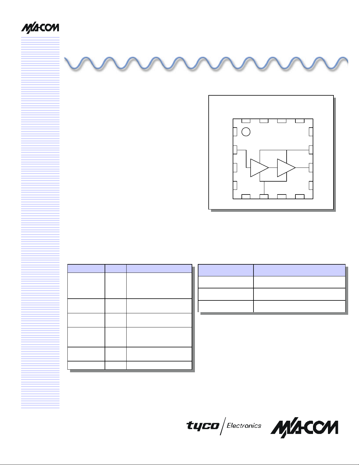
1-Watt Power Amplifier
Vdd
N/C
N/C
N/C
Vgg
MAAPSM0008
5 - 6 GHz
Features
• U-NII and Hiperlan Applications
• Saturated Output Power 30.5 dBm at +7.0 V
• Power Added Efficiency 40 Percent
• No External RF Matching
• 4-mm FQFP -N, 16 -Lead Package
Description
The MAAPSM0008 is a two-stage power amplifier
mounted in a standard outl ine, 16-lead, 4-mm FQFP -N
plastic package, designed specifically for the U-NII,
MMAC, and Hiperlan bands. The MAAPSM0008 has
fully matched 50 ohms input and output, eliminating
the need for external RF tuning components.
M/A-COM fabricates the MAAPSM0008 using a self aligned gate MESFET process to realize high power
efficiency and small size. The process features full
passivation for performance and reliability.
MAAPSM0008
Functional Schematic
Pin 16
N/C
Pin 1
RFin
N/C
N/C N/C N/C
V 1.1
N/C
RFout
N/C
N/CN/C
Pin Configuration
Pin Function
1, 3, 4 ,5 ,7,
8, 9, 12, 13,
14, 15, 16
2 RFIN RF input to the amplifier. DC
6 Vdd Positive voltage supply to
10 RF
11 Vgg Negative voltage supply to
Pad GND RF & DC ground
NC No connection
Specifications subject to change without notice.
n North America: Tel. (800) 366-2266, Fax (800) 618-8883
n Asia/Pacific: Tel.+81-44-844 -8296, Fax +81-44-844-8298
n Europe: Tel. +44 (1344) 869 595, Fax+44 (1344) 300 020
Visit www.macom.com for additional data sheets and product information.
Descriptions
block on-chip. 50 ohm input.
both stages
RF output of the amplifier.
OUT
DC block on-chip. 50 Ohm
output.
the gates of both stages
Ordering Information
Part Number Package
MAAPSM0008TR MAAPSM0008 on 7-inch, 1000-piece reel
MAAPSM0008TR-3000 MAAPSM0008 on 13 inch, 3000-piece reel
MAAPSM0008SMB MAAPSM0008 Sample Test Board
Page 2
1-Watt, 5 GHz Power Amplifier
MAAPSM0008
V 1.1
Electrical Specifications: T
= 40 °C, VDD = 7.0 V, IDQ = 360 mA
C
(unless otherwise specified)
Parameter Test Conditions Units Min. Typ. Max. Typ. @
VDD + 5 V
Frequency GHz 5.0 6.0
Input VSWR F = 5.825 GHz, Pin = +14 dBm 1.5:1 2.0:1 1.5:1
Gain F = 5.825 GHz, Pin = 0 dBm dB 18.0 19.5 19.0
P1dB F = 5.825 GHz dBm 29.5 28.0
Saturated Power F = 5.825 GHz, Pin = +14 dBm dBm 29.5 30.5 29.0
Drain Current at Psat F = 5.825 GHz, Pin = +14 dBm mA 500 600 500
Harmonics 2ƒ
Thermal resistance °C/W 31 31
Third-Order Intercept
Point
Stability +3.0 V < V
3 ƒ
Output Power = 30.5 dBm dBc
dBm 40 38
< +10.0 V, P
dBm, VSWR < 6:1, -25 ºC < TC < 70
ºC, RBW = 3 MHz max. hold
DD
OUT
< +15
dBc
-40
-70
All spurs < -70 dBc
-40
Recommended Operating Conditions
Characteristic Symbol Unit Min Typ Max
Drain Voltage V
Gate Voltage 2 V
Input Power P
Gate Current I
Case Temperature T
DD
GG
IN
GG
C
1
V 4.5 7.0 8.0
V -2.5 -2.0 -1.0
dBm — 15
mA -4 1 +4
°C -40 25 70
-70
1. Operation outside of these ranges may reduce product reliability.
2. A 100 E-Series resistor should be used in the gate voltage line.
Operating The MAAPSM0008
The MAAPSM0008 is static sensitive. Please handle
with care. To operate the device, follow these steps.
1. Apply VGG = -2 V, VDD= 0 V.
2. Ramp VDD to desired voltage, typically 5 to 7 V.
3. Adjust VGG to set IDQ, (approximately –2 V).
4. Set RF input.
5. Power down sequence in reverse. Turn gate
voltage off last.
Specifications subject to change without notice.
n North America: Tel. (800) 366-2266, Fax (800) 618-8883
n Asia/Pacific: Tel.+81-44-844 -8296, Fax +81-44-844-8298
n Europe: Tel. +44 (1344) 869 595, Fax+44 (1344) 300 020
Visit www.macom.com for additional data sheets and product information.
2
Page 3

1-Watt, 5 GHz Power Amplifier
C1 R1
Plated Vias
Application Information
Sample Board
Notes on board design
1. Sample board uses RO4350 er = 3.48 as dielectric for circuit board. Dielectric thickness is not
critical but RFin and RFout transmission lines
should be 50 ohms (w = 22 mi l for thickness = 10
mil).
2. Solder the exposed paddle on the back of the
package to the board. Proper attachment of the
exposed paddle is essential for RF and DC
ground in addition to providing a low thermal resistance.
3. Case temperature (Tc) is measured as shown on
the application board drawing on the top circuit
board metal as close to the body of the package
as possible.
4. The board must provide adequate heat sinking to
accommodate the 2.5 W typically dissipated under small signal conditions. Sample board uses
vias in the vicinity of the ground pad to provide a
suitable heat sink connected to the ground plane
of the board as shown above (recommend
theta
5. Placement of C1, C2 and R1 are not critical but
use of 1206 for the bypass caps (C1 and C2) is
critical.
= 5 °C/W max).
CA
Plated
C2
MAAPSM0008
V 1.1
Vias
Specifications subject to change without notice.
n North America: Tel. (800) 366-2266, Fax (800) 618-8883
n Asia/Pacific: Tel.+81-44-844 -8296, Fax +81-44-844-8298
n Europe: Tel. +44 (1344) 869 595, Fax+44 (1344) 300 020
Visit www.macom.com for additional data sheets and product information.
3
Page 4

1-Watt, 5 GHz Power Amplifier
Output Power
(dBm)
FREQUENCY (GHz
)
Output Power (
dBm)
PAE (%)
16 18 20 22 24
FREQUENCY (GHz)
12
22
FREQUENCY (GHz)
Typical Performance Curves
MAAPSM0008
V 1.1
GAIN (dB)
Gain Vs. Frequency
PIN = + 6 dBm, VDD = 7 V
14
12
10
4.0
4.5
5.0
5.5
Output Power Vs. Frequency
PIN = + 12 dBm, VDD = 7 V
32
30
28
- 25 deg. C
50 deg. C
70 deg. C
6.0
6.5
Gain Vs. Frequency
PIN = + 6 dBm, VDD = 5 V
24
20
18
16
GAIN (dB)
14
10
4.0
4.5
5.0
Output Power Vs. Frequency
PIN = + 12 dBm, VDD = 5 V
32
30
28
5.5
- 25 deg. C
50 deg. C
70 deg. C
6.0
6.5
26
24
4.0
4.5
5.0
5.5
- 25 deg. C
50 deg. C
70 deg. C
6.0
6.5
PAE Vs. Frequency
PIN = + 12 dBm, VDD = 7 V
45
40
35
PAE (%)
30
25
4.0
Specifications subject to change without notice.
n North America: Tel. (800) 366-2266, Fax (800) 618-8883
n Asia/Pacific: Tel.+81-44-844 -8296, Fax +81-44-844-8298
n Europe: Tel. +44 (1344) 869 595, Fax+44 (1344) 300 020
Visit www.macom.com for additional data sheets and product information.
4.5
5.0
FREQUENCY (GHz)
5.5
- 25 deg. C
50 deg. C
70 deg. C
6.0
6.5
26
24
4.0
4.5
5.0
FREQUENCY (GHz)
5.5
- 25 deg. C
6.5
50 deg. C
70 deg. C
6.0
PAE Vs. Frequency
PIN = + 12 dBm, VDD = 5 V
45
40
35
30
25
4.0
4.5
5.0
FREQUENCY (GHz)
5.5
- 25 deg. C
50 deg. C
70 deg. C
6.0
6.5
4
Page 5

1-Watt, 5 GHz Power Amplifier
Typical Performance Curves
MAAPSM0008
V 1.1
Input Return Loss Vs. Frequency
PIN = + 12 dBm, VDD = 7 V
-3
-6
-9
-12
-15
-18
-21
RETURN LOSS (dB)
-24
-27
4.0 4.5 5.0 5.5 6.0 6.5
FREQUENCY (GHz)
Dissipated Power vs. Case
Temperature
P
vs Channel Temperature (Tc)
Diss
4.5
4
3.5
3
2.5
(W)
2
Diss
P
1.5
1
0.5
0
0 25 50 75 100 125 150 175
Tc (C)
- 25 deg. C
50 deg. C
70 deg. C
Input Return Loss Vs. Frequency
PIN = + 12 dBm, VDD = 5 V
-3
-6
-9
-12
-15
-18
-21
RETURN LOSS (dB)
-24
-27
4.0 4.5 5.0 5.5 6.0 6.5
FREQUENCY (GHz)
- 25 deg. C
50 deg. C
70 deg. C
Output Power & Gain Vs. Input Power
Freq = 5.80 GHz, VDD = 7 V
35
30
25
20
Pout (dBm), Gain (dB)
15
1 3 5 7 9 11 13 15
Pin (dBm)
Pout
Gain
1-dB Compression Vs. Frequency
VDD = 7 V, IDq = 0.360 A
32
30
28
P1dB (dBm)
26
24
5.0 5.2 5.4 5.6 5.8 6.0
Pin (dBm)
Specifications subject to change without notice.
n North America: Tel. (800) 366-2266, Fax (800) 618-8883
n Asia/Pacific: Tel.+81-44-844 -8296, Fax +81-44-844-8298
n Europe: Tel. +44 (1344) 869 595, Fax+44 (1344) 300 020
Visit www.macom.com for additional data sheets and product information.
P1dB
P1dB, Gain Vs. Quiescent Bias
VDD = 7 V, Freq = 5.8 GHz
32
30
28
26
24
22
20
Gain (dB), P1dB (dBm)
18
0.20 0.22 0.24 0.26 0.28 0.30 0.32 0.34 0.36
IDQ (A)
P1dB
Gain
5
Page 6

1-Watt, 5 GHz Power Amplifier
4- mm FQFP-N, 16-Lead (MLP)
Package, Saw Singulated
MAAPSM0008
V 1.1
E
3 x e
D
16
1
2
3
4
A
A2
A1
PIN #1
16 x b
IDENTIFIER
D2
e
E2
L
Dim
Min. Nom. Max.
A 0.80 0.90 1.00
A1 0 0.02 0.05
A2 0.80 0.88 1.00
b 0.23 0.30 0.38
D - 4.00 basic -
D2 2.05 2.15 2.25
e 0.65 basic
E - 4.00 basic E2 2.05 2.15 2.25
L 0.45 typ. 0.55 typ. 0.65 typ.
Note: See JEDEC MO -220A VGGC Issue B for additional
dimensional and tolerance information.
Measurement (mm)
e
3 x e
Handling Procedures
Please observe the following precautions to avoid
damage to the MAAPSM0008:
Static Sensitivity
Gallium arsenide integrated circuits are ESD sensitive
and can be damaged by static electricity. Use proper
ESD precautions when handling these devices.
Specifications subject to change without notice.
n North America: Tel. (800) 366-2266, Fax (800) 618-8883
n Asia/Pacific: Tel.+81-44-844 -8296, Fax +81-44-844-8298
n Europe: Tel. +44 (1344) 869 595, Fax+44 (1344) 300 020
Visit www.macom.com for additional data sheets and product information.
Absolute Maximum Ratings1
Parameter Absolute Maximum
Max Input Power (5 - 6 GHz)
Operating Voltages +10 volts
Operating Temperature
Channel Temperature
Storage Temperature -40 °C to +150 °C
1. E xceeding any one or combination of these limits may cause
permanent damage.
+ 15 dBm
-40 °C to +70 °C
+150 °C
6
 Loading...