

Page 1

MA5332MS
200W Stereo, Integrated Class D Amplifier
Features
2 channel analog input Class D audio amplifier in a small 7x7mm package
Very low R
95% efficiency Class D at 2x200W at 4Ω
Split or single power supply capable
Differential or single-ended input
Multiple configuration options: 2xSE, BTL, PSE (Parallel Single-Ended)
Over-current, over-temperature and under-voltage protections with self-reset feature
Start/stop click noise reduction
Clip and Fault reporting outputs
Applications
Multi-channel home theatre system
Studio monitor
Active speaker
Soundbar subwoofer
Marine amplifier
Aftermarket car audio system
General-purpose audio power amplifier
Product validation
at 24.4 mΩ typical, enabling heatsink-less operation at 2x100W at 4Ω
DS(ON)
Total Harmonic Distortion
PG- IQFN-42
Qualified for standard applications according to the
relevant tests of J-STD-020 and JESD22.
Product type Package
MA5332MS 7x7mm PG- IQFN-42
Description
The MA5332MS offers the same or higher output power than monolithic alternatives without heatsink and 50%
less footprint. This MCM (multi-chip module) solution integrates 2 channel PWM controller, high voltage gate
driver, and 4 low R
features for reliable operation over various environmental conditions. As a powerful upgrade to IR43x2M and
other monolithic solutions, MA5332MS’ 7x7 mm PG- IQFN-42 package showcases the benefit of small footprint,
high power density, and heatsink-less operation.
Topology Half-bridge / Full bridge
MA5332MS Output power (Halfbridge,THD+N=10%, typical)
*Residual noise (AES-17, IHF-A, typical) 250 μVrms
*THD+N (1kHz, 70W, 4 Ω, typical) 0.01 %
* In a typical application
MOSFETs. Like its predecessor, IR43x2M, it includes standard Class D protection
DS(ON)
150 W in 2 Ω / 300 W in 4 Ω
200 W in 4 Ω / 400 W in 8 Ω
160 W in 6 Ω
Datasheet Please read the Important Notice and Warnings at the end of this document V 2.0
www.infineon.com page 1 of 59 9/24/2021
Page 2

MA
5332MS
Table of contents
Integrated Class D Amplifier
Table of contents
Features ........................................................................................................................................ 1
Applications ................................................................................................................................... 1
Product validation .......................................................................................................................... 1
Description .................................................................................................................................... 1
Table of contents ............................................................................................................................ 2
1 Qualification information ........................................................................................................ 4
2 Device Comparison Table ........................................................................................................ 5
3 Pin Configuration ................................................................................................................... 6
3.1 Lead assignments .................................................................................................................................... 6
3.2 Lead definitions ....................................................................................................................................... 7
4 Specifications ........................................................................................................................ 8
4.1 Absolute maximum ratings ..................................................................................................................... 8
4.2 Recommended operating conditions ..................................................................................................... 9
4.3 Electrical characteristics ....................................................................................................................... 10
4.4 Audio characteristics (SE) ..................................................................................................................... 13
4.5 Audio characteristics (BTL) ................................................................................................................... 13
4.6 Audio characteristics (PSE) ................................................................................................................... 14
4.7 Typical Audio characteristics (SE) ........................................................................................................ 15
4.7.1 Power vs. THD+N .............................................................................................................................. 15
4.7.2 Frequency vs. THD+N ....................................................................................................................... 16
4.7.3 Frequency response ......................................................................................................................... 16
4.7.4 Noise floor ........................................................................................................................................ 17
4.7.5 Efficiency .......................................................................................................................................... 17
4.8 Typical Audio characteristics (BTL) ...................................................................................................... 18
4.8.1 Power vs. THD+N .............................................................................................................................. 18
4.8.2 Frequency vs. THD+N ....................................................................................................................... 19
4.8.3 Frequency response ......................................................................................................................... 19
4.8.4 Noise floor ........................................................................................................................................ 20
4.9 Typical Audio characteristics (PSE) ...................................................................................................... 21
4.9.1 Power vs. THD+N .............................................................................................................................. 21
4.9.2 Frequency vs. THD+N ....................................................................................................................... 22
4.9.3 Frequency response ......................................................................................................................... 22
4.9.4 Noise floor ........................................................................................................................................ 23
5 Thermal information ............................................................................................................. 24
5.1 Peak power duration thermal information .......................................................................................... 24
5.2 Heatsink information ............................................................................................................................ 28
6 Functional block diagram ....................................................................................................... 29
7 Typical Implementation ......................................................................................................... 30
8 Input / Output pin equivalent circuit diagrams ......................................................................... 33
9 PWM Modulator Design .......................................................................................................... 34
9.1 Input Section ......................................................................................................................................... 34
9.2 Control Loop Design .............................................................................................................................. 35
9.3 PWM Frequency ..................................................................................................................................... 35
9.4 Clock Synchronization .......................................................................................................................... 36
9.5 Click Noise Elimination ......................................................................................................................... 37
Datasheet 2 of 59 V 2.0
9/24/2021
Page 3

MA
5332MS
Table of contents
Integrated Class D Amplifier
9.6 Differential Input ................................................................................................................................... 38
10 Operational Mode.................................................................................................................. 39
10.1 Self-oscillation Start-up Condition ....................................................................................................... 39
11 Protections ........................................................................................................................... 40
11.1.1 Self-Reset Protection ....................................................................................................................... 41
11.1.2 Designing Ct...................................................................................................................................... 42
11.1.3 Shutdown Input ............................................................................................................................... 42
11.1.4 Latched Protection........................................................................................................................... 43
11.1.5 Interfacing with System Controller ................................................................................................. 43
11.2 Over Current Protection (OCP) ............................................................................................................. 44
11.3 Over Temperature Protection (OTP) .................................................................................................... 45
11.4 Under Voltage Protection (UVP) ........................................................................................................... 45
12 Status Output ....................................................................................................................... 46
12.1 Fault Output .......................................................................................................................................... 46
12.2 CLIP Output ........................................................................................................................................... 47
13 Power Supply Design ............................................................................................................. 48
13.1 Supplying VAA and VSS ......................................................................................................................... 48
13.2 Supplying VCC and VB ........................................................................................................................... 48
13.2.1 Choosing Bootstrap Capacitance .................................................................................................... 49
13.2.2 Choosing Bootstrap Diode ............................................................................................................... 49
13.2.3 Charging VBS Prior to Start ................................................................................................................ 49
13.3 Power Supply Sequence ....................................................................................................................... 51
14 Package details ..................................................................................................................... 52
15 Board mounting, part marking, and ordering information ......................................................... 55
Revision history............................................................................................................................. 60
Datasheet 3 of 59 V 2.0
9/24/2021
Page 4
MA
5332MS
Table of contents
Integrated Class D Amplifier
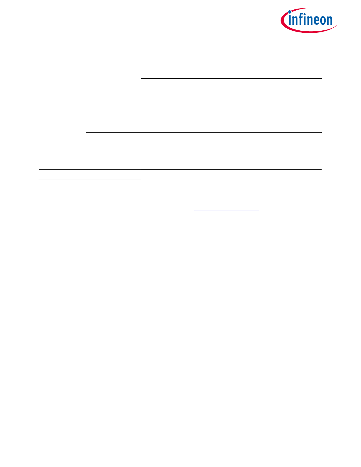
1 Qualification information
Qualification Level (1) Standard (2)
Qualified for standard applications according to the relevant tests
of J-STD-020 and JESD22
Moisture Sensitivity Level (MSL) (3) MSL3
(per IPC/JEDEC J-STD-020)
ESD Charge Device
Model
Human Body
Model
IC Latch-Up Test
RoHS Compliant Yes
Class C2a
(per JEDEC standard JS-002)
Class 1B
(per JEDEC standard JS-001)
Class I, Level A
(per JESD78)
Note:
1. Qualification standards can be found at Infineon’s web site
2. Higher qualification ratings may be available should the user have such requirements. Please contact your
http://www.infineon.com/
International Rectifier sales representative for further information.
3. Higher MSL ratings may be available for the specific package types listed here. Please contact your International
Rectifier sales representative for further information.
Datasheet 4 of 59 V 2.0
9/24/2021
Page 5

MA
5332MS
Table of contents
Integrated Class D Amplifier
2 Device Comparison Table
Table 1
Device Name Description
MA5332MS 200W (4 Ω)*2 channel integrated analog input Class D audio Amplifier
IR4302M 130W (4 Ω)*2 channel integrated analog input Class D audio Amplifier
IR4322M 100W (2 Ω)*2 channel integrated analog input Class D audio Amplifier
IR4312M 35W (4 Ω)*2 channel integrated analog input Class D audio Amplifier
IR4301M 160W (4 Ω) single-channel integrated analog input Class D audio Amplifier
IR4321M 135W (2 Ω) single-channel integrated analog input Class D audio Amplifier
IR4311M 35W (4 Ω) single-channel integrated analog input Class D audio Amplifier
Datasheet 5 of 59 V 2.0
9/24/2021
Page 6

MA
5332MS
Table of contents
Integrated Class D Amplifier
3 Pin Configuration
3.1 Lead assignments
Figure 1 Lead assignments
Datasheet 6 of 59 V 2.0
9/24/2021
Page 7

MA
5332MS
Table of contents
outputs.
Integrated Class D Amplifier
3.2 Lead definitions
Pin # Symbol
1 CLIP Clipping detection output, open drain, referenced to GND
2 COMP2 CH2 PWM comparator input
3 IN-2 CH2 Analog inverting input
4 IN+2 CH2 Analog non-inverting input
5 GND
6 VSS Floating input negative supply
7 VAA Floating input positive supply
8 IN+1 CH1 Analog non-inverting input
9 IN-1 CH1 Analog inverting input
10 COMP1 CH1 PWM comparator input
11 CSD Shutdown timing capacitor / shutdown input
12 FAULT Fault reporting output, open drain, referenced to GND
13 VCC Low side supply
14 COM Low side supply return, internally connected to pin 27
15 CSH1 CH1 High side over current sensing input, referenced to VS1
16 VB1 CH1 High side floating supply
17 VS1 CH1 PWM output, internally connected to pin 19
18 VP1 CH1 Positive power supply
19 VS1 CH1 PWM output
20 VN1 CH1 Negative power supply, connect to COM externally
21 VN2 CH2 Negative power supply, connect to COM externally
22 VS2 CH2 PWM output, internally connected to pin 24
23 VP2 CH2 Positive power supply
24 VS2 CH2 PWM output
25 VB2 CH2 High side floating supply
26 CSH2 CH2 High side over current sensing input, referenced to VS2
27 COM Low side supply return, internally connected to pin 14
28 NC
Description
GND for internal shunt zener diodes to VAA and VSS, a reference to FAULT and CLIP
Datasheet 7 of 59 V 2.0
9/24/2021
Page 8
MA
5332MS
Table of contents
Integrated Class D Amplifier
4 Specifications
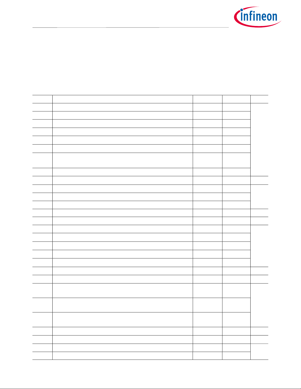
4.1 Absolute maximum ratings
Absolute Maximum Ratings indicate sustained limits beyond which damage to the device may occur. All
voltage parameters are absolute voltages referenced to COM=VN1=VN2; all currents are defined positive into
any lead. The Thermal Resistance and Power Dissipation ratings are measured under board mounted and still
air conditions.
Symbol
VPn Positive power supply rail voltage, n=1-2
Definition Min Max Units
- 100
VBn High side floating supply voltage -0.3 115
VSn
V
CSHn
V
CC
VAA
VSS
V
IN+n
I
INn
V
CSD
V
COMPn
V
CLIP
I
CLIP pin sinking current
CLIP
V
FAULT
I
FAULT
I
AAZ
I
SSZ
I
CCZ
I
BSZn
High side floating supply voltage
CSH pin input voltage, n=1-2
Low side supply voltage
(2)
Floating input positive supply voltage
Floating input negative supply voltage
Floating input supply ground voltage , n=1-2 VSS -0.3 VAA +0.3
Input current between IN- and IN+ pins
CSD pin input voltage
COMP pin input voltage, n=1-2
CLIP pin input voltage
FAULT pin input voltage GND -0.3 VAA +0.3 V
FAULT pin sinking current
Floating input supply zener clamp current
Floating input negative supply zener clamp current
Low side supply zener clamp current
Floating supply zener clamp current
dVSn/dt Allowable Vs voltage slew rate, n=1-2
dVSS/dt
Id
@ 25ºC
Allowable Vss voltage slew rate
Continuous output current, from VPn to VSn, VSn to VNn,
VCC=10V, VBn-VSn=10V
Id
Continuous output current, from VPn to VSn, VSn to VNn,
@ 100ºC
VCC=10V, VBn-VSn=10V
IDM Pulsed output current, from VPn to VSn, VSn to VNn, VCC=10V,
VBn-VSn=10V
Pd
RthJC
T
Control IC junction temperature - 150
JIC
T
JFET
Power dissipation
Thermal resistance, junction to case
FET junction temperature - 150
(5)
(4)
@ TC = 25C
(2)
(3)
(4)
, n=1-2
(2)
(2)
(1)
(2)
(2)
, n=1-2
, n=1-2
(2)
V
-15 V
Bn
VSn -0.3 V
Bn
Bn
-0.3 15
-0.3 110
-1
(See I
SSZ
)
GND +0.3
- ±3 mA
VSS -0.3 VAA +0.3
VSS -0.3 VAA +0.3
GND -0.3 VAA +0.3
- 5 mA
- 5
- 20
(2)
- 20
- 20
- 20
- 50 V/ns
- 50 V/ms
- 16
- 10
- 64
- 25
- 5
+0.3
+0.3
V
mA
A
W
C/W
C
Datasheet 8 of 59 V 2.0
9/24/2021
Page 9
MA
5332MS
T
able of contents
VBn
High side floating supply absolute voltage, n=1
-2
VSn
+10 VSn +14
VAA
Floating input positive supply voltage
VSS
+9.0
VSS + 9.8
I
AAZ
Floating input supply zener clamp current
1 15
I
SSZ
Floating input negative supply zener clamp current
1 15 V
CC
Low side fixed supply voltage
10 15
VIC IN- and IN+ pins co
mmon mode input voltage
V
SS
+ 2 VAA - 2
V
IN-n
Inverting input voltage, n=1
-2
V
IN+
-0.5 V
IN+
+0.5 V
CSD
CSD pin input voltage
VSS
VAA
V
COMPn
COMP
pin input voltage, n=1
-2
VSS
VAA
V
CS
Hn
CSH pin input voltage, n=1
-2
VSn
VBn V
fSW
Switching f
requency
-
500 kHz
T
J_IC
Juction temperature of controller IC
-40 100
C
Integrated Class D Amplifier
TS Storage Temperature -55 150
TL Lead temperature (Soldering, 10 seconds) - 300
Note:
1. IN- and IN+ contain clamping diodes between the two pins.
2. VAA -VSS, Vcc-COM and VBn-VSn contain internal shunt zener diodes. Note that the voltage ratings of these can be limited by
the clamping current.
3. For the rising and falling edges of step signal of 10V. Vss=15V to 100V.
4. Per MOSFET.
5. Repetitive rating, pulse width limited by maximum junction temperature.
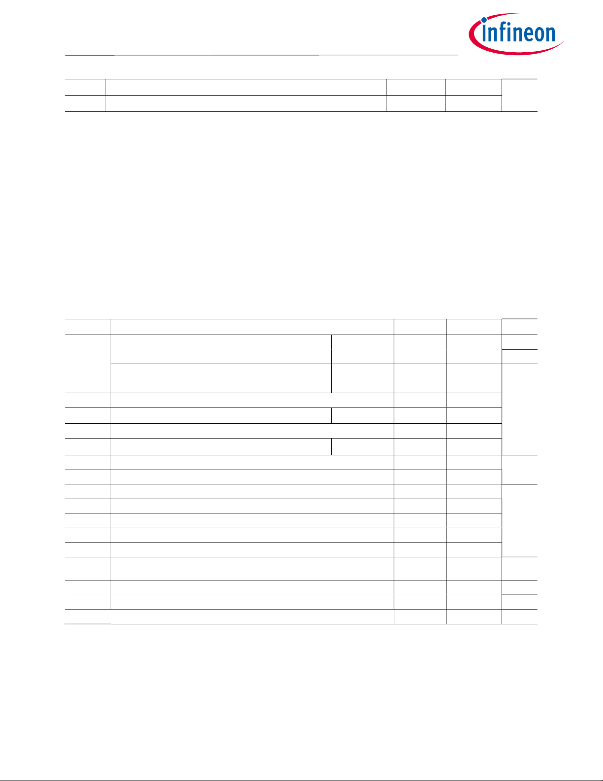
4.2 Recommended operating conditions
For proper operation, the device should be used within the recommended conditions below. The Vss and Vsn
offset ratings are tested with supplies biased at COM=VN1=VN2, VAA-VSS=9.6V, VCC=12V and VBn-VSn=12V. All
voltage parameters are absolute voltages referenced to COM; all currents are defined positive into any lead.
Symbol Definition Min Max Units
Positive power supply voltage, n=1-2, without
heatsink
MA5332MS - 60
VPn
Positive power supply voltage, n=1-2, with
heatsink
VSn High side floating supply offset voltage, n=1-2 MA5332MS
(7)
VSS
Floating input negative supply voltage
(7)
(7)
MA5332MS - 80
(6)
100
MA5332MS 0 100
(7)
V
mA
V
C
COMP pin phase compensation capacitor to GND , n=1-2 1 - nF
COMPn
Note:
6. Logic operational for Vs equal to –5V to +100V. Logic state held for Vs equal to –5V to –VBS.
7. GND input voltage is limited by I
Datasheet 9 of 59 V 2.0
9/24/2021
AAZ
and I
SSZ
.
Page 10
MA
5332MS
Table of contents
Integrated Class D Amplifier
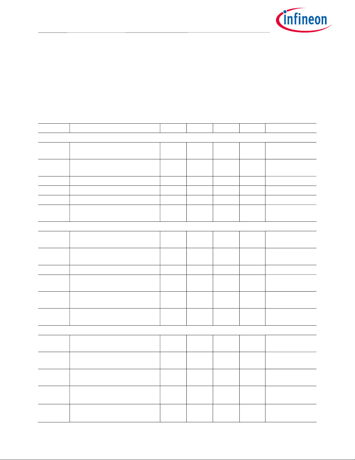
4.3 Electrical characteristics
Unless otherwise specified, the following apply:
V
V
V
T
= 12 V
CC,VBS
SS=VS1=VS2=VN1=VN2
=9.6V
AA
=25C
A
=COM=0V
Table 2 Electrical characteristics
Symbol Definition Min Typ Max Units Test conditions
Low-side supply
UV
CC+
UV
CC-
UV
CCHYS
I
Low side quiescent current - - 3 mA
QCC
Vcc supply UVLO positive
threshold
Vcc supply UVLO negative
threshold
UV
hysteresis - 0.2 - V
CC
8.4 8.9 9.4 V
8.2 8.7 9.2 V
ICC Low side supply current - 10 - mA f=400kHz
V
CLAMPL
n
Low side zener diode clamp
voltage, n=1-2
14.7 15.3 16.2 V ICC=5mA
High-side floating supply
UV
BS+n
UV
BS-n
UV
BSHYSn
I
QBSn
I
QBSn_OFF-CSH
V
CLAMPHn
High side well UVLO positive
threshold, n=1-2
High side well UVLO negative
threshold, n=1-2
UV
hysteresis, n=1-2 - 0.2 - V
BS
High side quiescent current,
n=1-2
High side quiescent current,
with CSH pin open n=1-2
High side zener diode clamp
voltage, n=1-2
8.0 8.5 9.0 V
7.8 8.3 8.8 V
- - 2.4 mA
350 500 650 uA
14.7 15.3 16.2 V IBS=5mA
Floating input supply
UV
UV
UV
I
QAA0
I
QAA1
AA+
AA-
UV
AAHYS
VA+, VA- floating supply UVLO
positive threshold from VSS
VA+, VA- floating supply UVLO
negative threshold from VSS
hysteresis - 0.5 - V
AA
Floating Input positive quiescent
supply current
Floating Input positive quiescent
supply current
8.2 8.7 9.2 V
7.7 8.2 8.7 V
- 1.5 3 mA
- 4 6 mA
VSS =0V, GND pin
floating
VSS =0V, GND pin
floating
VSS =0V, GND pin
floating
VAA=9.6V, VSS =0V,
V
=VSS
CSD
VAA=9.6V, VSS =0V,
V
=VAA
CSD
Datasheet 10 of 59 V 2.0
9/24/2021
Page 11
MA
5332MS
Table of contents
Integrated Class D Amplifier
I
I
QAA2
LKM
Floating Input positive quiescent
supply current
Floating input side to Low side
leakage current
- 5 7.5 mA
- - 50 µA
VAA floating supply zener diode
V
CLAMPM+
clamp voltage, positive, with
4.9 5.1 5.4 V
respect to GND
VSS floating supply zener diode
V
CLAMPM-
clamp voltage, negative, with
-5.4 -5.1 -4.9 V
respect to GND
Audio input (V
V
Input offset voltage, n=1-2 -18 0 18 mV
OSn
I
Input bias current, n=1-2 - - 40 nA
BINn
GBWn
gmn OTA transconductance, n=1-2 - 10 - mS
GVn OTA gain, n=1-2 50 - - dB
V
Nrmsn
=0, VAA=4.8V, VSS=-4.8V)
GND
Small signal bandwidth in OTA, n=12
CHn OTA input noise voltage,
n=1-2
- 9 - MHz C
- 200 330 mVrms
PWM
Vth
f
OTAn
PWM
PWM comparator threshold in
COMP
COMP pin star-up local oscillation
frequency, n=1-2
-
0.7 1.0 1.5 MHz V
(VAA VSS)/2
- V
VAA=9.6V, VSS =0V,
V
=GND
CSD
VAA=VSS=V
GND
=
100V
IAA=5mA,
ISS=5mA,
V
=0V,
GND
V
=VSS
CSD
IAA=5mA,
ISS=5mA,
V
=0V,
GND
V
=VSS
CSD
=1nF, Rf=0
COMP
V
=0V, V
IN+
=10mV
CSD
IN-
=GND
Ton_n
Toff_n
DTn
COMP to VS rising edge propagation
delay, n=1-2
COMP to VS trailing edge
propagation delay, n=1-2
Deadtime: Low-side turn-off to
High-side turn-on (DT
LO-HO
) & Highside turn-off to Low-side turn-on
(DT
) , n=1-2
HO-LO
- 370 - ns
- 320 - ns
- 50 - ns
VP=30V,
VN=-30V,
Power MOSFET (FET1, FET2, FET3, FET4)
At Tj=25°C, unless otherwise specified
(8)
V
(BR)DSS
R
FET on resistance - 24.4 30.5 mΩ
DS(ON)
Drain-to-Source breakdown voltage 100 - - V
Qg Total gate charge - 12.7 19 nC
I
VP leakage current, VS=VN - - 20 µA
LK0
VGS=0V,
ID=250uA
ID=3.3A, VGS=10V
VGS=10V
CSD
=VSS
(8)
,
VP=100V
V
Protection
Datasheet 11 of 59 V 2.0
9/24/2021
Page 12

MA
5332MS
Table of contents
Integrated Class D Amplifier
I
OCPn
I
OCNn
Vth1
Over current detection Positive
threshold, n=1-2
(8)
Over current detection Negative
threshold, n=1-2
(9)
CSD pin shutdown release
threshold
- 40 - A
- -40 - A
0.62xVAA 0.70xVAA 0.78xVAA V
Vth2 CSD pin self-reset threshold 0.26xVAA 0.30xVAA 0.34xVAA V
I
CSD pin discharge current 70 100 130 µA
CSD+
I
CSD pin charge current 70 100 130 µA
CSD-
t
SDn
t
OCPn
t
OCNn
Vth+
Vth-
t
CLIP
t
CLIPmin
TSD
T
SDHYS
CLIP
CLIP
Shutdown propagation delay from
VS < Vth1 to Shutdown, n=1-2
CHn propagation delay time from
IOn > I
to Shutdown, n=1-2
OCPn
CHn propagation delay time from
IOn < I
Clip detection positive threshold in
COMP
to Shutdown, n=1-2
OCNn
Clip detection negative threshold in
COMP
Clipping detection propagation
delay
Clipping detection minimum output
duration
Over-temperature shutdown
threshold in controller IC
Over-temperature shutdown
threshold hysteresis
- - 250 ns
- - 500 ns
- - 500 ns
0.85xVAA 0.90xVAA 0.95xVAA V
0.05xVAA 0.10xVAA 0.15xVAA V
- 40 - ns
- 3 - us
100 - - ºC
- 7 - ºC
V
= VSS +4.8V
CSD
V
= VSS +4.8V
CSD
COMP = VSS
COMP = VSS
COMP = VSS
Datasheet 12 of 59 V 2.0
9/24/2021
Page 13
MA
5332MS
Table of contents
Integrated Class D Amplifier
4.4 Audio characteristics (SE)
Table 3
Parameter Test conditions Typ Unit
Po Power output per channel
Residual noise(AES-17, IHF-A,
typical)
Idling supply current
Efficiency
(11)
(10)
RL= 6Ω, 10%THD+N, V
RL= 4Ω, 10%THD+N, V
RL= 3Ω, 10%THD+N, V
RL= 2Ω, 10%THD+N, V
RL= 6Ω, 1%THD+N, V
RL= 4Ω, 1%THD+N, V
RL= 3Ω, 1%THD+N, V
RL= 2Ω, 1%THD+N, V
EVAL_AUDAMP25 , V
EVAL_AUDAMP25 , V
EVAL_AUDAMP25, V
Pout=200W, RL= 4Ω
= ± 40 V
bus
= ± 36.5 V
bus
= ± 31.5 V
bus
= ± 23 V
bus
= ± 40 V
bus
= ± 36.5 V
bus
= ± 31.5 V
bus
= ± 23V
bus
= ± 36.5 V ,RL= 4Ω
bus
= ± 36.5 V ,RL= 4Ω
bus
= ± 36.5 V,
bus
160 W
200
190
150
120
150
140
110
250 uV
+55 mA
-80
95 %
Note:
8. Vp changes over temperature at a rate of 50mV/K compared to Tj=25°C.
9. Over-current protection threshold measured under Tj=25°C condition.
10. Tested with heatsink (digikey part number: V8818V)
11. Class D stage only
4.5 Audio characteristics (BTL)
Table 4
Parameter Test conditions Typ Unit
Po Power output per channel
Residual noise(AES-17, IHF-A,
typical)
Idling supply current
Efficiency
(10)
(9)
RL= 8Ω, 10%THD+N, V
RL= 6Ω, 10%THD+N, V
RL= 4Ω, 10%THD+N, V
RL= 8Ω, 1%THD+N, V
RL= 6Ω, 1%THD+N, V
RL= 4Ω, 1%THD+N, V
EVAL_AUDAMP25 , V
EVAL_AUDAMP25 , V
= ± 36.5 V
bus
= ± 31.5 V
bus
= ± 23 V
bus
= ± 36.5 V
bus
= ± 31.5 V
bus
= ± 23V
bus
= ± 36.5 V ,RL= 4Ω 350 uV
bus
= ± 36.5 V ,RL= 8Ω
bus
EVAL_AUDAMP25 , V
= ± 36.5 V ,RL= 8Ω
bus
400 W
380
300
300
280
220
+55 mA
-80
95 %
Datasheet 13 of 59 V 2.0
9/24/2021
Page 14
MA
5332MS
Table of contents
Integrated Class D Amplifier
4.6 Audio characteristics (PSE)
Table 5
Parameter Test conditions Typ Unit
Po Power output per channel
Residual noise(AES-17, IHF-A,
typical)
Idling supply current
Efficiency
(10)
(9)
RL= 2Ω, 10%THD+N, V
RL= 2Ω, 1%THD+N, V
EVAL_AUDAMP25 , V
EVAL_AUDAMP25 , V
EVAL_AUDAMP25 , V
= ± 36.5 V
bus
= ± 36.5V
bus
= ± 36.5 V ,RL= 4Ω
bus
= ± 36.5 V ,RL= 4Ω
bus
= ± 36.5 V ,RL= 4Ω
bus
400 W
300
250 uV
+55 mA
-80
95 %
Datasheet 14 of 59 V 2.0
9/24/2021
Page 15
MA
5332MS
Table of contents
Integrated Class D Amplifier
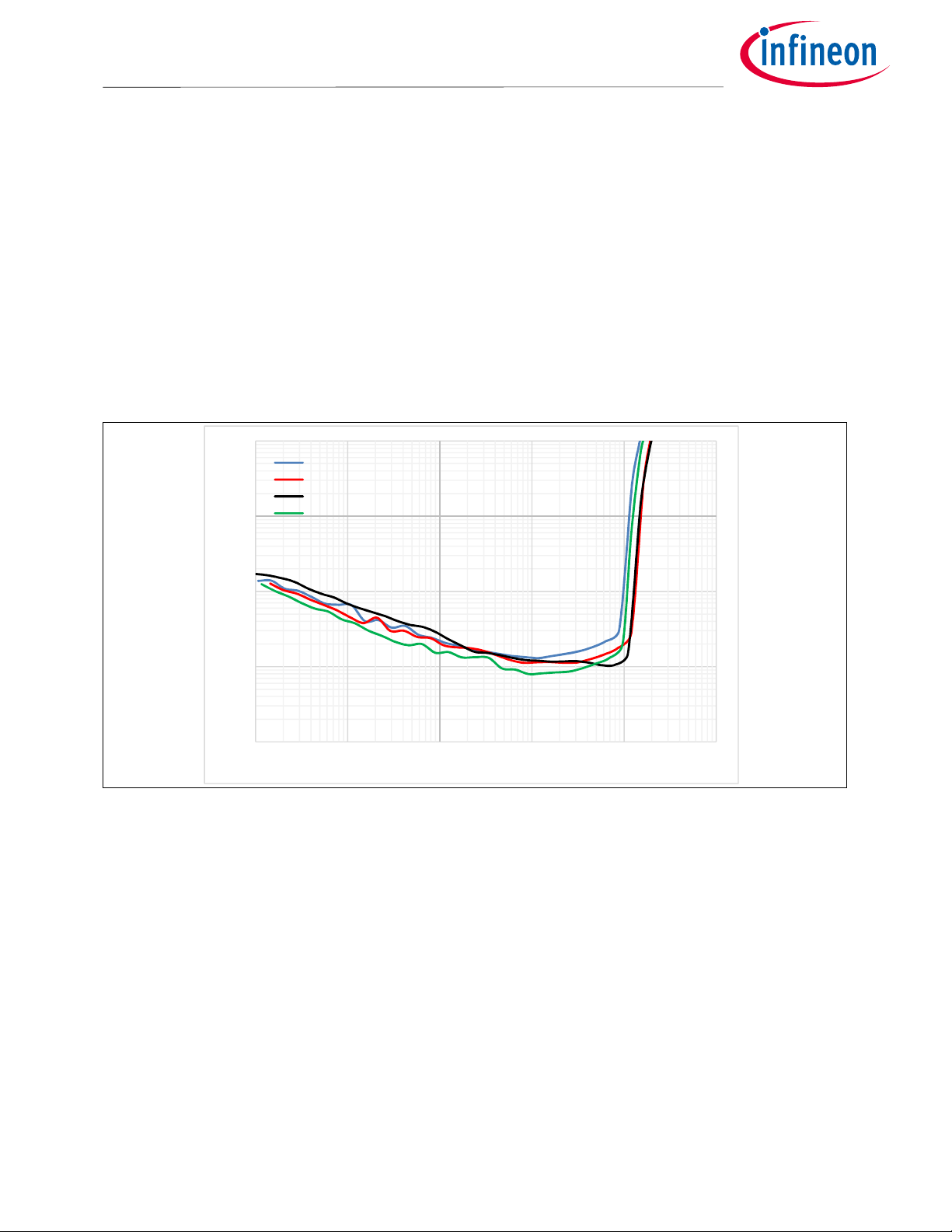
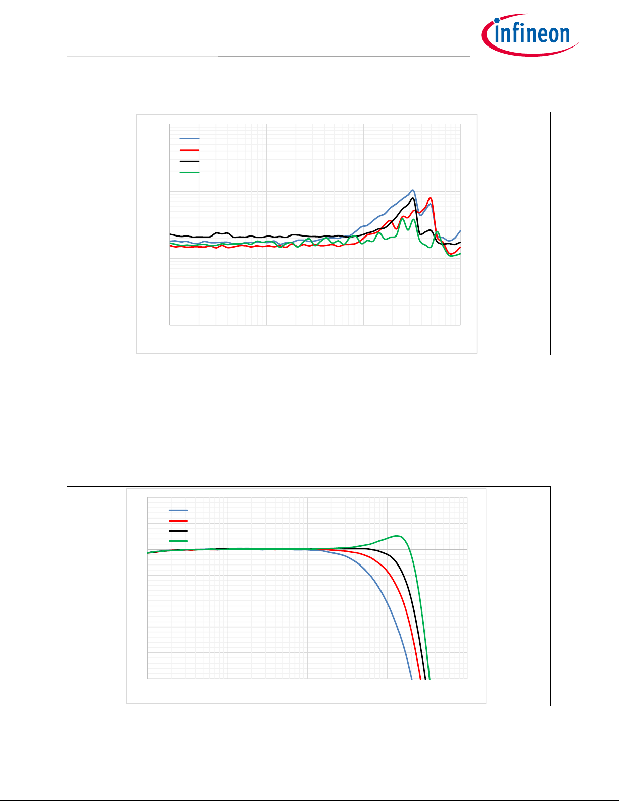
4.7 Typical Audio characteristics (SE)
Test conditions:
All Measurements taken at Sine wave frequency= 1 kHz, AES17+ AUX-0025 measurement filters.
V
= ± 40 V, Load impedance = 6 Ω, F
bus
V
= ± 36.5 V, Load impedance = 4 Ω, F
bus
V
= ± 31.5 V, Load impedance = 3 Ω, F
bus
V
= ± 23 V, Load impedance = 2 Ω, F
bus
= 400 kHz
PWM
= 400 kHz
PWM
= 400 kHz
PWM
= 400 kHz
PWM
4.7.1 Power vs. THD+N
10
2ohm
3ohm
4ohm
1
6ohm
0.1
THD+N(%)
0.01
0.001
0.01 0.1 1 10 100 1000
Figure 2 Power vs. THD+N
Outpower(W)
Datasheet 15 of 59 V 2.0
9/24/2021
Page 16
MA
5332MS
Table of contents
Integrated Class D Amplifier
4.7.2 Frequency vs. THD+N
1
2ohm
3ohm
4ohm
6ohm
0.1
THD+N(%)
0.01
0.001
20 200 2000 20000
Figure 3 Frequency vs. THD+N @1W
4.7.3 Frequency response
Test conditions:
Output power = 1 W, LPF = 22uH+0.47uF
4
2ohm
2
0
-2
dBr A
-4
3ohm
4ohm
6ohm
Frequency(Hz)
Figure 4 Frequency response
Datasheet 16 of 59 V 2.0
9/24/2021
-6
-8
-10
20 200 2000 20000 200000
Frequency(Hz)
Page 17

MA
5332MS
Table of contents
Integrated Class D Amplifier
4.7.4 Noise floor
10
-10
-30
-50
dBV
-70
-90
-110
-130
-150
10 100 1000 10000
Figure 5 Noise floor
4.7.5 Efficiency
2ohm
3ohm
4ohm
6ohm
Frequency(Hz)
100.0%
90.0%
80.0%
70.0%
60.0%
50.0%
40.0%
Efficiency
30.0%
20.0%
10.0%
0.0%
0.00 50.00 100.00 150.00 200.00 250.00
Figure 6 Efficiency 4 Ω load
MA5332 4ohm load
MA5332 4ohm load
Power (W)
Datasheet 17 of 59 V 2.0
9/24/2021
Page 18
MA
5332MS
Table of contents
10
Integrated Class D Amplifier
4.8 Typical Audio characteristics (BTL)
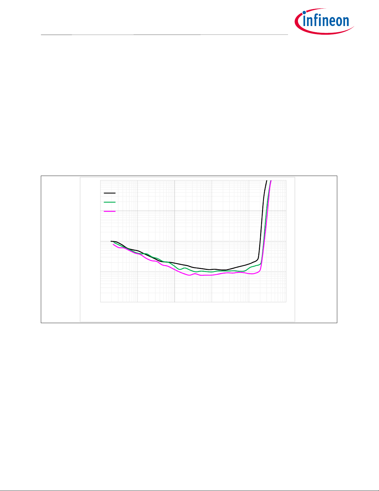
Test conditions:
All Measurements taken at Sine wave frequency= 1 kHz, AES17+ AUX-0025 measurement filters.
V
= ± 40 V, Load impedance = 8 Ω, F
bus
V
= ± 31.5 V, Load impedance = 6 Ω, F
bus
V
= ± 23 V, Load impedance = 4 Ω, F
bus
= 400 kHz
PWM
= 400 kHz
PWM
= 400 kHz
PWM
4.8.1 Power vs. THD+N
4ohm
6ohm
1
0.1
THD+N(%)
0.01
0.001
0.01 0.1 1 10 100 1000
8ohm
Figure 7 Power vs. THD+N
Outpower(W)
Datasheet 18 of 59 V 2.0
9/24/2021
Page 19
MA
5332MS
Table of contents
Integrated Class D Amplifier
4.8.2 Frequency vs. THD+N
1
4ohm
6ohm
8ohm
0.1
THD+N(%)
0.01
0.001
20 200 2000 20000
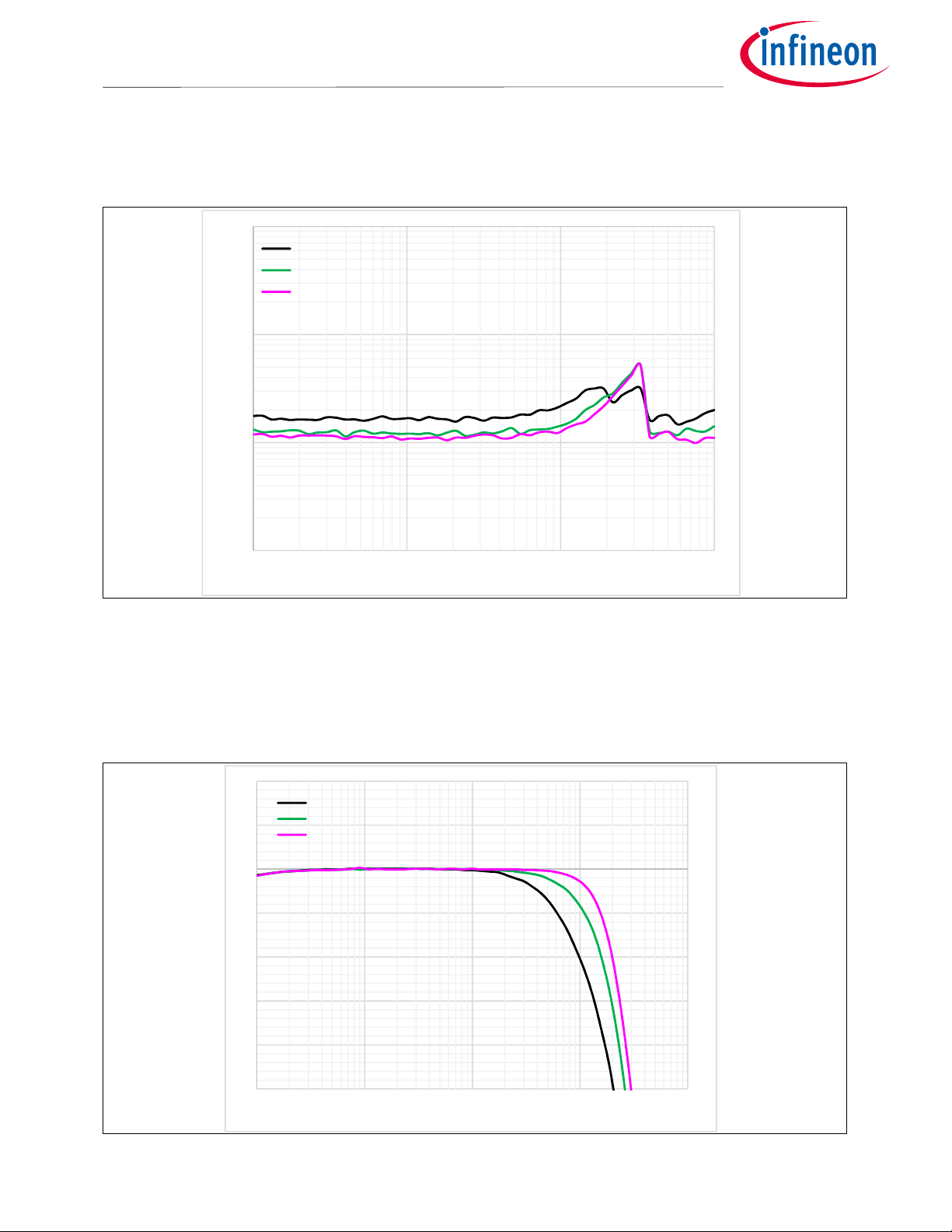
Figure 8 Frequency vs. THD+N @1W
4.8.3 Frequency response
Test conditions:
Output power = 1 W, fixed LPF 22uH+0.47uF
4
4ohm
2
0
-2
dBr A
-4
-6
6ohm
8ohm
Frequency(Hz)
Figure 9 Frequency response
Datasheet 19 of 59 V 2.0
9/24/2021
-8
-10
20 200 2000 20000 200000
Frequency(Hz)
Page 20
MA
5332MS
Table of contents
Integrated Class D Amplifier
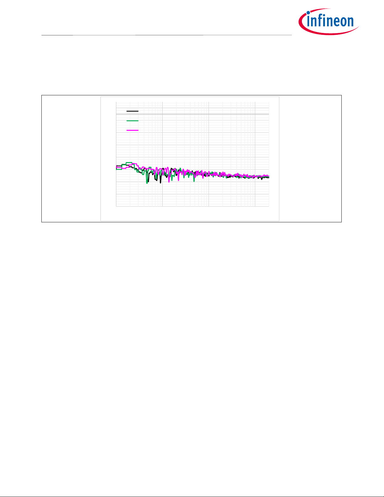
4.8.4 Noise floor
Test conditions:
No input signal
10
-10
-30
-50
-70
dBV
-90
-110
-130
-150
10 100 1000 10000
Figure 10 Noise floor
4ohm
6ohm
8ohm
Frequency(Hz)
Datasheet 20 of 59 V 2.0
9/24/2021
Page 21
MA
5332MS
Table of contents
10
Integrated Class D Amplifier
4.9 Typical Audio characteristics (PSE)
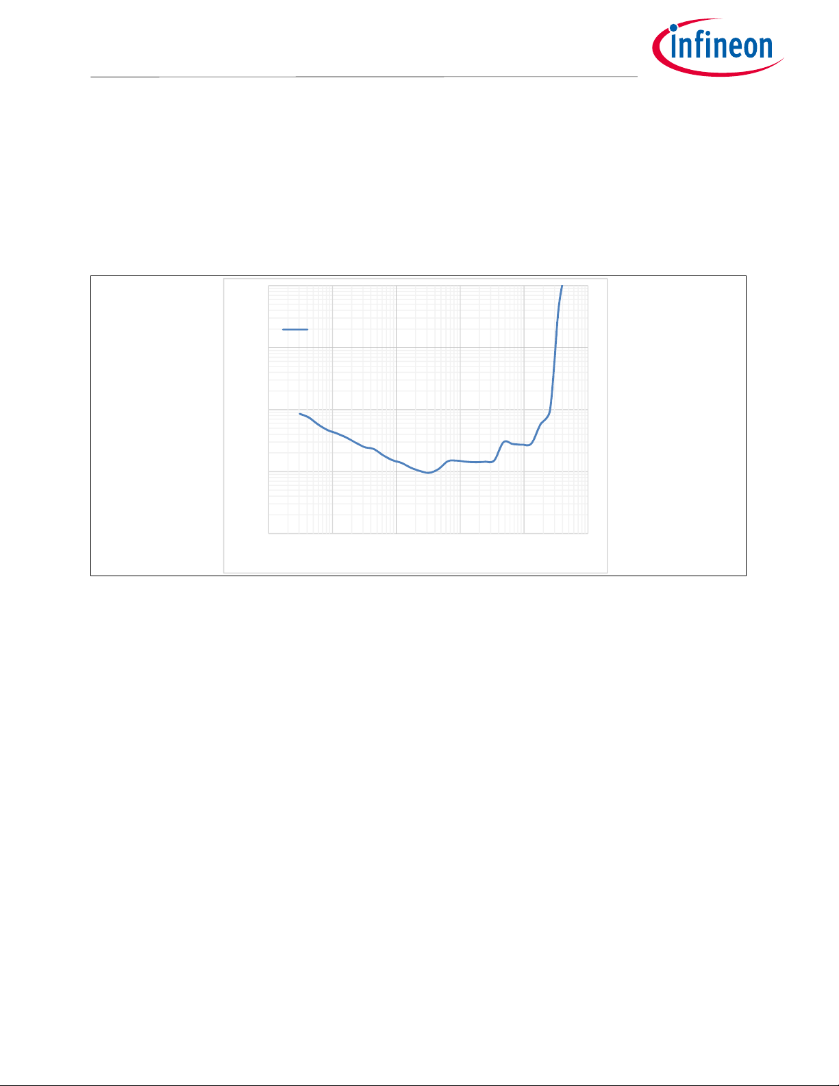
Test conditions:
All Measurements taken at Sine wave frequency= 1 kHz, AES17+ AUX-0025 measurement filters.
V
= ± 36.5 V, Load impedance = 2 Ω, F
bus
= 400 kHz
PWM
4.9.1 Power vs. THD+N
2ohm
1
0.1
THD+N(%)
0.01
0.001
0.01 0.1 1 10 100 1000
Figure 11 Power vs. THD+N
Outpower(W)
Datasheet 21 of 59 V 2.0
9/24/2021
Page 22
MA
5332MS
Table of contents
Integrated Class D Amplifier
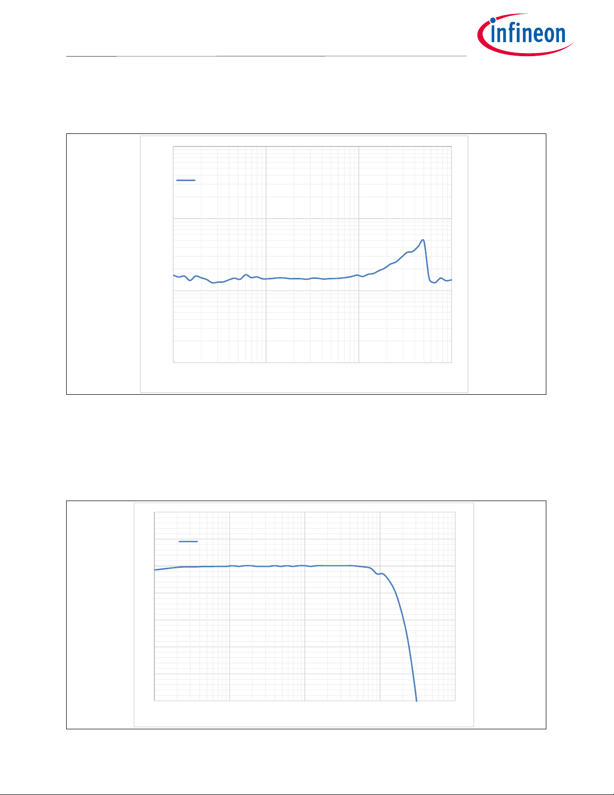
4.9.2 Frequency vs. THD+N
1
2ohm
0.1
THD+N(%)
0.01
0.001
20 200 2000 20000
Figure 12 Frequency vs. THD+N @1W
4.9.3 Frequency response
Test conditions:
Output power = 1 W, fixed LPF 22uH+0.47uF
4
2
0
-2
dBr A
-4
-6
2ohm
Frequency(Hz)
Figure 13 Frequency response
Datasheet 22 of 59 V 2.0
9/24/2021
-8
-10
20 200 2000 20000 200000
Frequency(Hz)
Page 23
MA
5332MS
Table of contents
Integrated Class D Amplifier
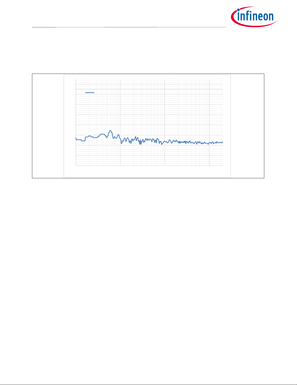
4.9.4 Noise floor
Test conditions:
No input signal
10
-10
-30
-50
-70
dBV
-90
-110
-130
-150
10 100 1000 10000
Figure 14 Noise floor
2ohm
Frequency(Hz)
Datasheet 23 of 59 V 2.0
9/24/2021
Page 24
MA
5332MS
Tab
le of contents
±V
Integrated Class D Amplifier
5 Thermal information
Benefits from unique co-packaging technique and superior MOSFET technology, MA5332MS has the
best-in-class thermal performance, Peak power duration. It can deliver 100W*2/4Ω even without a heatsink.
5.1 Peak power duration thermal information
Test conditions:
All Measurements are taken at sinewave frequency= 1 kHz, AES17+ AUX-0025 measurement filters. Input signal
= 1 kHz, F
Tests are based on Eval_AUDAMP25 board when both channels are driven.
Table 6 Peak power with heatsink
= 400 kHz.
PWM
Load (Ω)
bus
(V)
10 percent THD+N power (W)
Duration
6 40 160 More than 1 minute without thermal shutdown
4 36.5 200
3 31.5 190
2 23 150
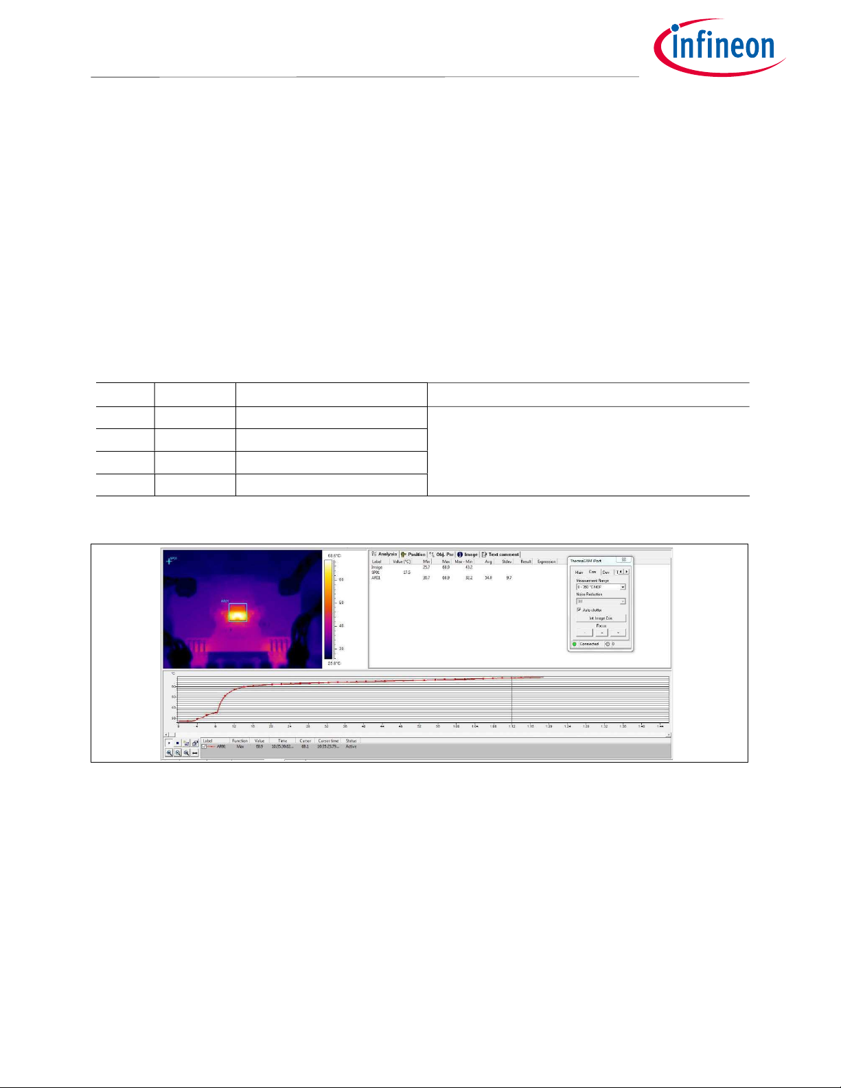
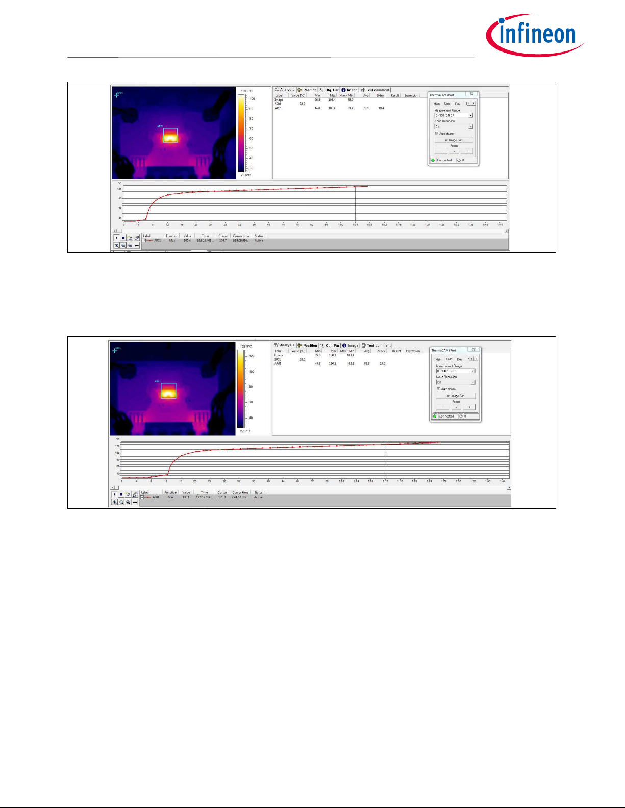
Figure 15 Peak power P
= 164 W with 6 Ω load ±40 V
out
Note: Maximum temperature 68.9°C at 1 minute.
Datasheet 24 of 59 V 2.0
9/24/2021
Page 25
MA
5332MS
Table of contents
Integrated Class D Amplifier
Figure 16 Peak power P
= 200 W with 4 Ω load ±36.5 V
out
Note: Maximum temperature 105°C at 1 minute.
Figure 17 Peak power P
= 194 W with 3 Ω load ±31.5 V
out
Note: Maximum temperature 130°C at 1 minute.
Datasheet 25 of 59 V 2.0
9/24/2021
Page 26
MA
5332MS
Table of contents
±V
Integrated Class D Amplifier
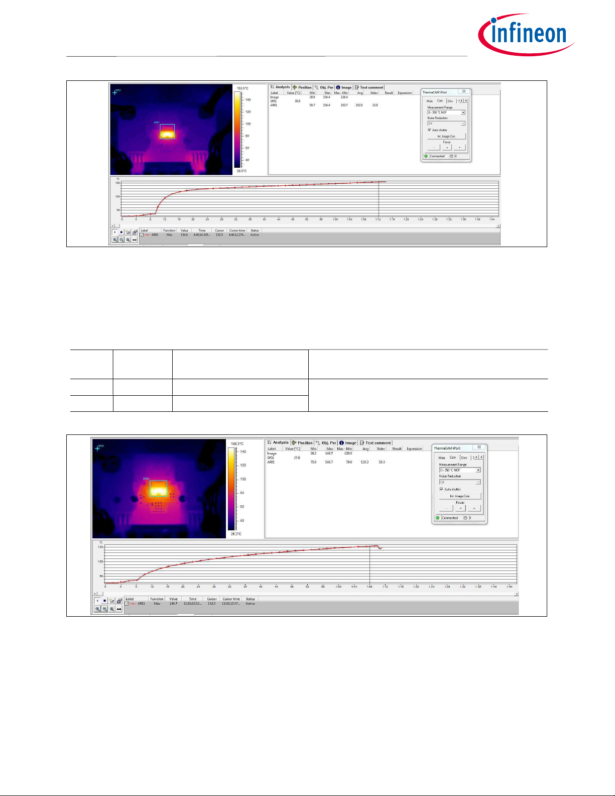
Figure 18 Peak power P
= 150 W with 2 Ω load ±23 V
out
Note: Maximum temperature 154°C at 1 minute.
Table 7 Peak power without heatsink
Load (Ω)
bus
(V)
10 percent THD+N power
Duration
(W)
4 26.5 100 More than 1 minute without thermal shutdown
2 13.7 50
Figure 19 Peak power P
Note: Maximum temperature 146.7°C at 1 minute.
Datasheet 26 of 59 V 2.0
9/24/2021
= 102 W with 4 Ω load ±26.5 V
out
Page 27
MA
5332MS
Table of contents
±V
±V
Integrated Class D Amplifier
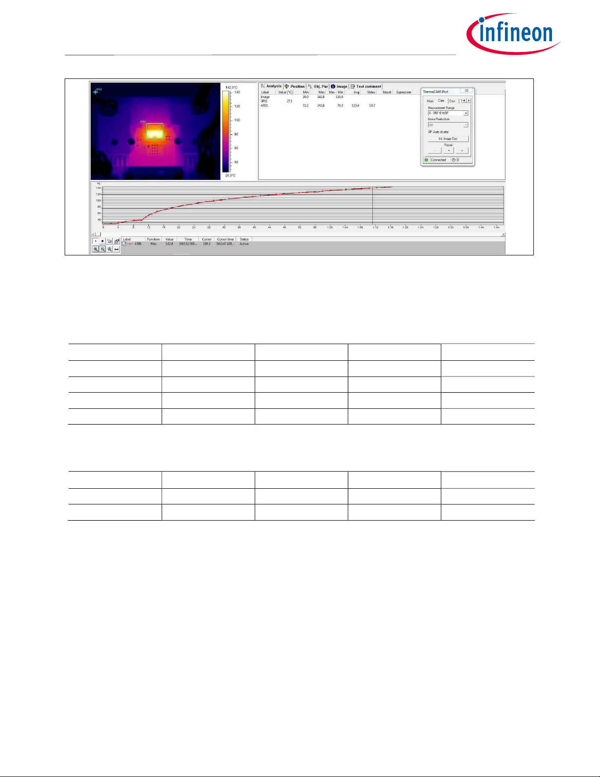
Figure 20 Peak power P
= 55 W with 2 Ω load ±13.7 V
out
Note: Maximum temperature 142.8°C at 1 minute.
Table 8 1/8 power test with heatsink
Load (Ω)
bus
(V)
Max. T-case (°C) 1/8 power (W) Duration (minutes)
6 40 71.6 16.5 30
4 36.5 85.6 19.8 30
3 31.5 87.2 19.7 30
2 23 84.8 15 30
Table 9 1/8 power test without heatsink
Load (Ω)
bus
(V)
Max. T-case (°C) 1/8 power (W) Duration (minutes)
4 22.7 84.6 7.12 30
2 13.7 76.1 4.88 30
Datasheet 27 of 59 V 2.0
9/24/2021
Page 28
MA
5332MS
Table of contents
Integrated Class D Amplifier
5.2 Heatsink information
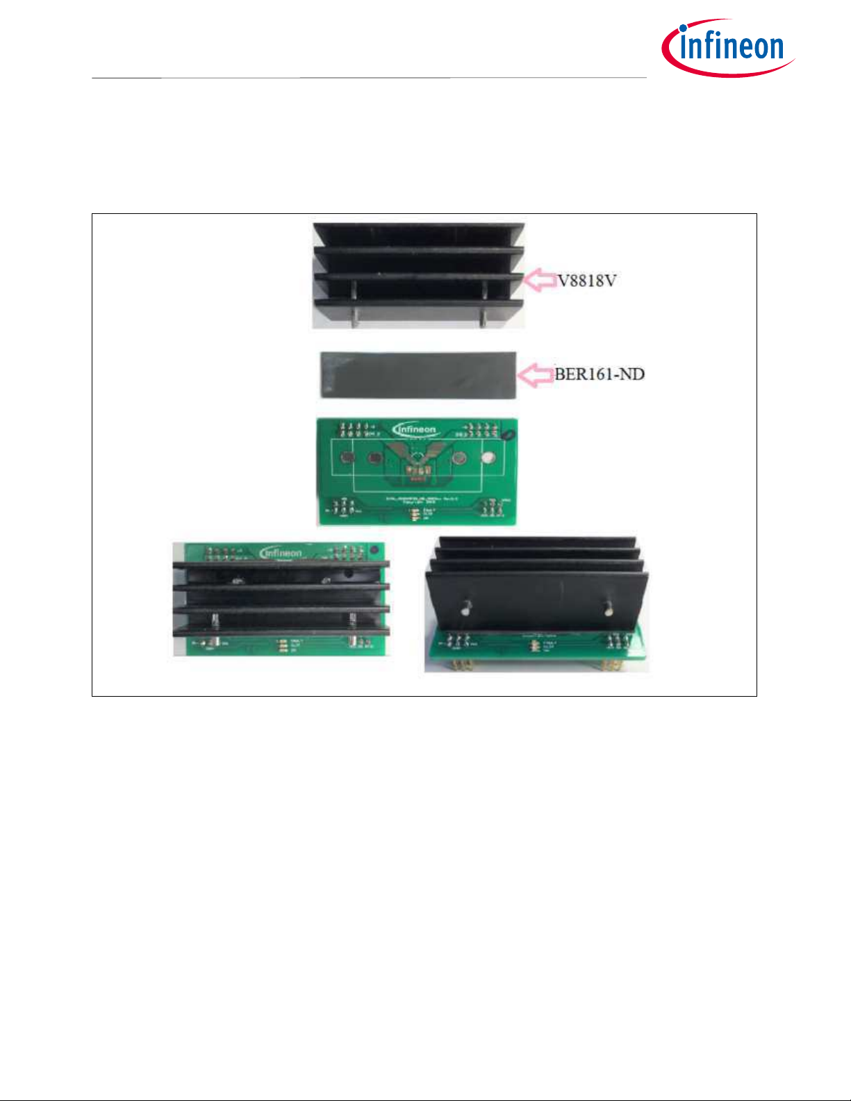
Heatsink: V8818V
Thermal pad: BER161-ND
Figure 21 Heatsink installation
Datasheet 28 of 59 V 2.0
9/24/2021
Page 29
MA
5332MS
Table of contents
Integrated Class D Amplifier
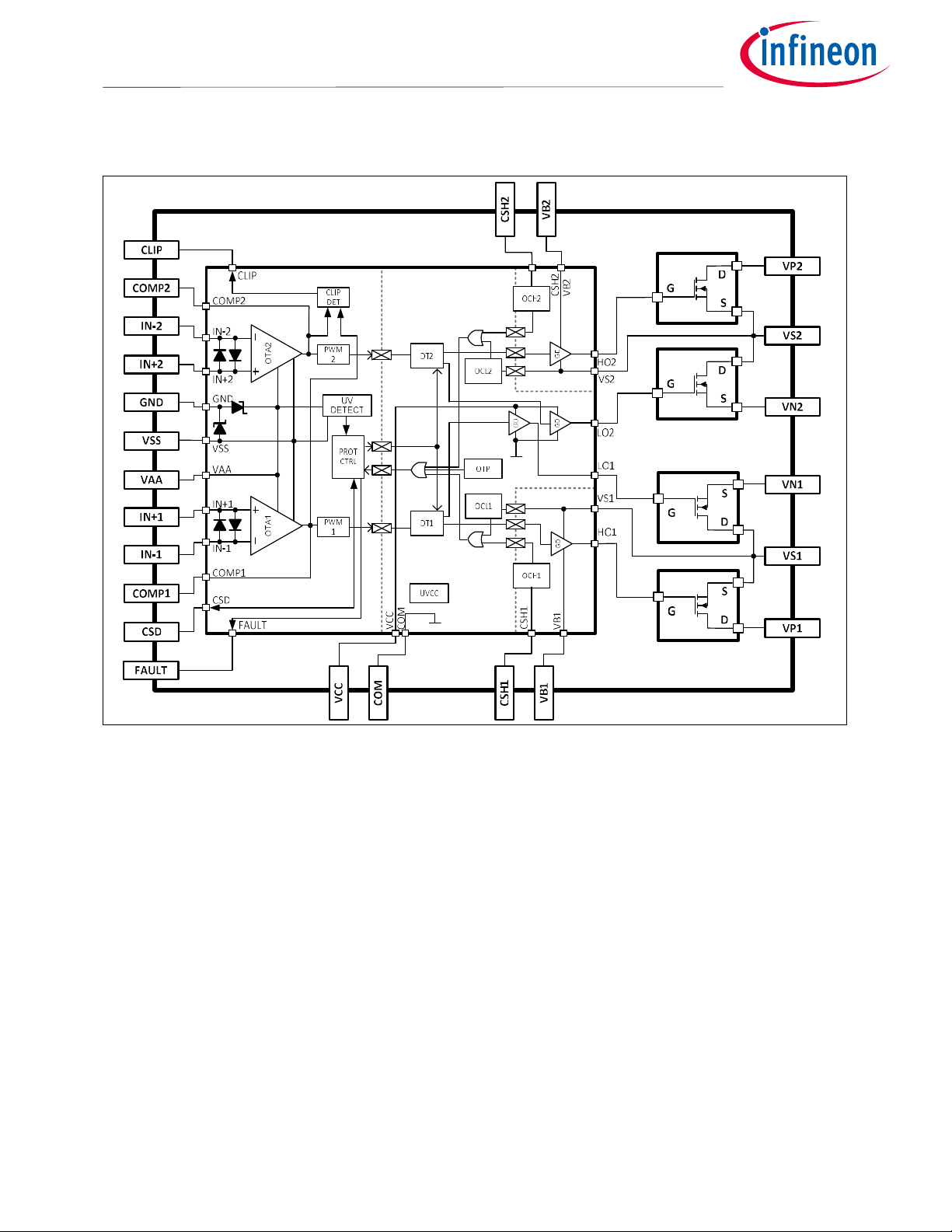
6 Functional block diagram
Figure 22 Block diagram
Datasheet 29 of 59 V 2.0
9/24/2021
Page 30
MA
5332MS
Table of contents
Integrated Class D Amplifier
7 Typical Implementation
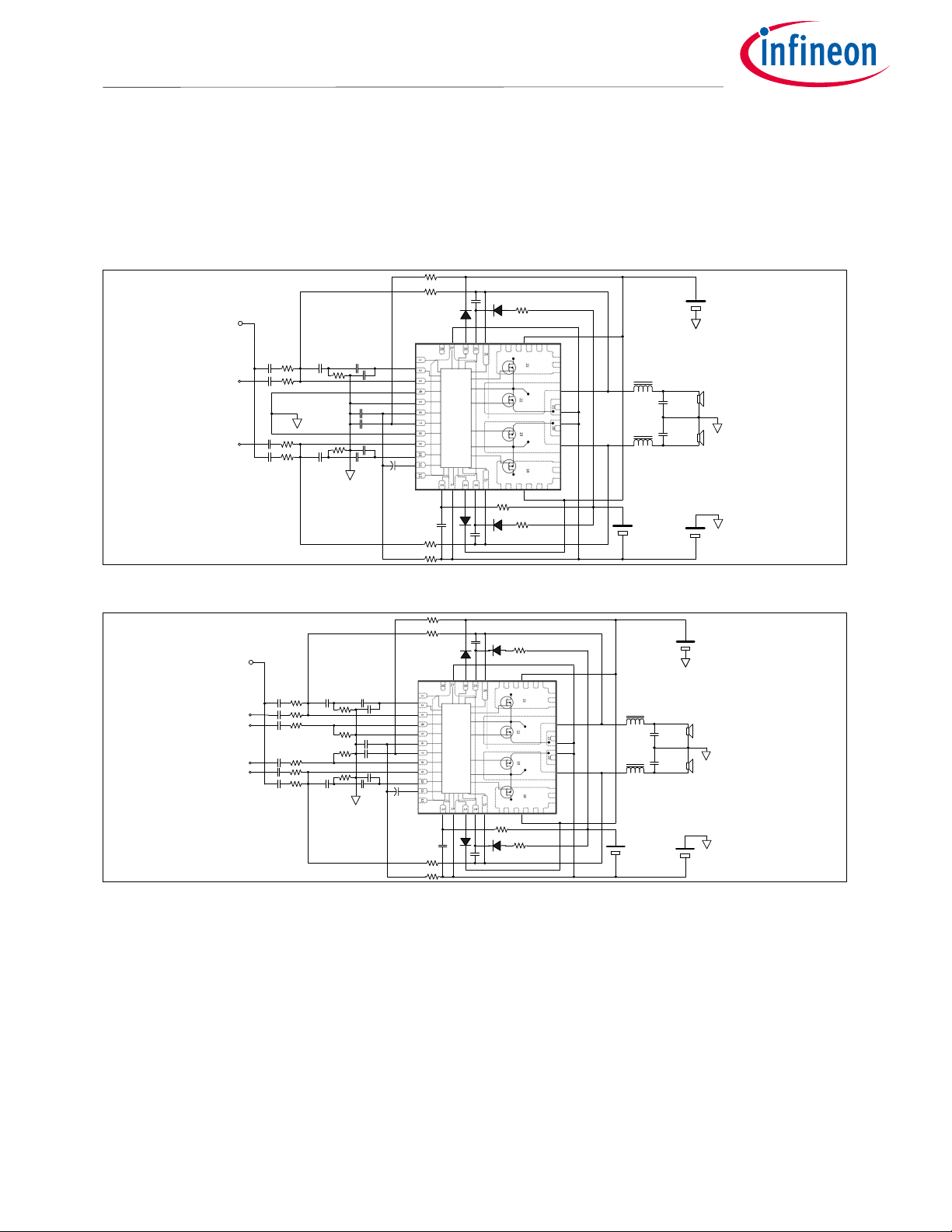
The MA5332MS can be designed as single-ended, BTL or parallel single ended (PSE) output configuration, using
a single or split power supply. Here are examples of typical configurations.
A configuration for single-ended input with split power supply sets the base example. The front end section
refers to GND which is common to speaker output GND.
EXT CLK
(OPTIONAL)
CH2 INPUT
CH1 INPUT
CLIP
COMP2
IN+2
GND
IN+1
COMP1
FAULT
IN-2
VSS
VAA
IN-1
CSD
CSH2
COM
VB2
VS2
COM
VCC
CSH1
VB1
VS1
Figure 23 Inverting amplifier with Split Power Supply
EXT CLK
(OPTIONAL)
CH2 IN+
CH2 IN-
CH1 IN-
CH1 IN+
CLIP
COMP2
GND
COMP1
FAULT
IN-2
IN+2
VSS
VAA
IN+1
IN-1
CSD
CSH2
COM
VB2
VS2
COM
VCC
CSH1
VB1
VS1
+B
VP2
VS2
VN2
VN1
VS1
VP1
VCC
CH2 OUTPUT
Speaker
Speaker
CH1 OUTPUT
-B
+B
VP2
VS2
VN2
VN1
VS1
VP1
CH2 OUTPUT
Speaker
Speaker
CH1 OUTPUT
Figure 24 Differential amplifier with Split Power Supply
Datasheet 30 of 59 V 2.0
9/24/2021
VCC
-B
Page 31
MA
5332MS
Table of contents
Integrated Class D Amplifier
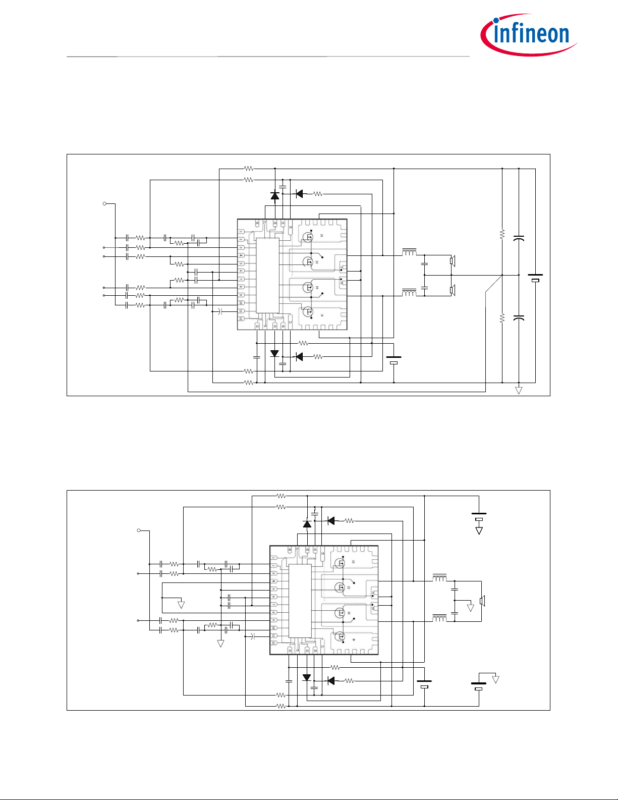
The single-supply configuration uses a virtual GND which sits in the middle of the power supply rail. The frontend section of the amplifier refers to the virtual GND as a reference. This method uses differential input to
receive an input signal from a different voltage potential. It is recommended to allow input capacitors to fully
settle to steady-state values before releasing the CSD pin to start PWM oscillation. The load current and
inductor ripple current flow through the bus splitting capacitor.
+B
EXT CLK
(OPTIONAL)
CH2 IN+
CH2 IN-
CH1 IN-
CH1 IN+
CLIP
COMP2
IN-2
IN+2
GND
VSS
VAA
IN+1
IN-1
COMP1
CSD
FAULT
CSH2
COM
VB2
VS2
VP2
VS2
VN2
VN1
VS1
COM
VCC
CSH1
VB1
VS1
VP1
VCC
CH2 OUTPUT
Speaker
Speaker
CH1 OUTPUT
Figure 25 Typical Application Circuit with Single Power Supply
Balanced Tied Load (BTL) output takes two output legs for speaker output. It doubles output power with
double load impedance. Any load current does not flow through supply dividing capacitor; therefore BTL
configuration is free from GND fluctuations. Also, the bus splitting capacitor can be much smaller. Higher
output power and absence of GND fluctuation make BTL suitable for subwoofer applications.
Figure 26 Typical Bridged Tied Load (BTL) Output Application with Split Power Supply
Datasheet 31 of 59 V 2.0
9/24/2021
EXT CLK
(OPTIONAL)
INPUT-
INPUT+
CLIP
COMP2
IN-2
IN+2
GND
VSS
VAA
IN+1
IN-1
COMP1
CSD
FAULT
+B
CSH2
COM
VB2
VS2
VP2
VS2
VN2
VN1
VS1
COM
VCC
CSH1
VB1
VS1
VP1
VCC
Speaker
-B
Page 32
MA
5332MS
Table of contents
Integrated Class D Amplifier
+B
EXT CLK
(OPTIONAL)
INPUT-
INPUT+
CLIP
COMP2
IN-2
IN+2
GND
VSS
VAA
10V
IN+1
IN-1
COMP1
CSD
FAULT
CSH2
COM
VB2
VS2
VP2
VS2
VN2
VN1
VS1
COM
VCC
CSH1
VB1
VS1
VP1
10V
Speaker
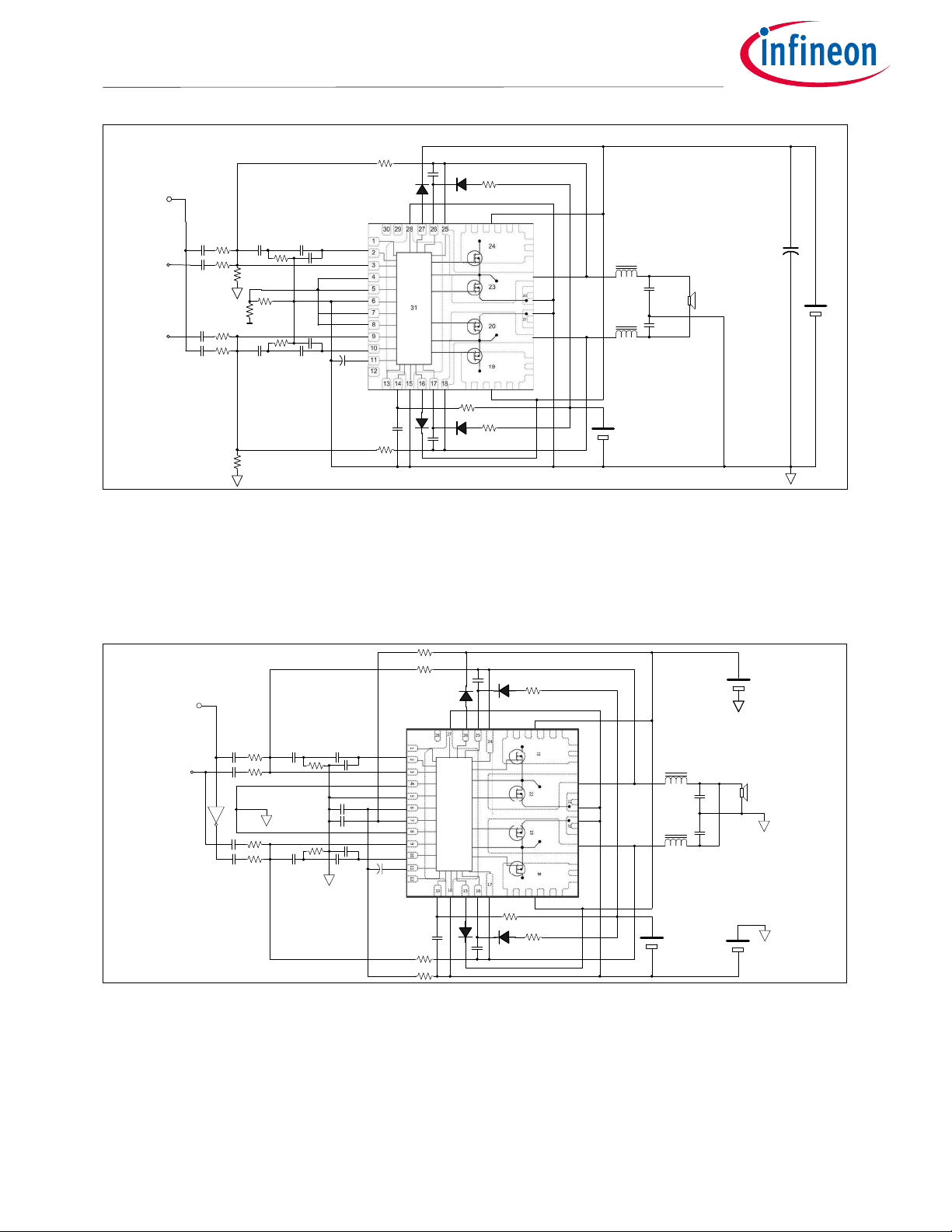
Figure 27 Typical Bridged Tied Load (BTL) Output Application with Single Power Supply
Parallel Single Ended (PSE) output parallels two channels’ output legs for one speaker output. It doubles
output current and makes it easier to drive a low impedance load. Higher output current with lower bus voltage
makes PSE suitable for subwoofer applications.
COM
CLIP
INPUT
COMP2
IN-2
IN+2
GND
VSS
VAA
IN+1
IN-1
COMP1
CSD
FAULT
COM
VCC
Figure 28 PSE amplifier with Split Power Supply
+B
CSH2
VB2
VS2
VP2
VS2
VN2
VN1
VS1
CSH1
VB1
VS1
VP1
VCC
Speaker
-B
Datasheet 32 of 59 V 2.0
9/24/2021
Page 33
MA
5332MS
Table of contents
Integrated Class D Amplifier
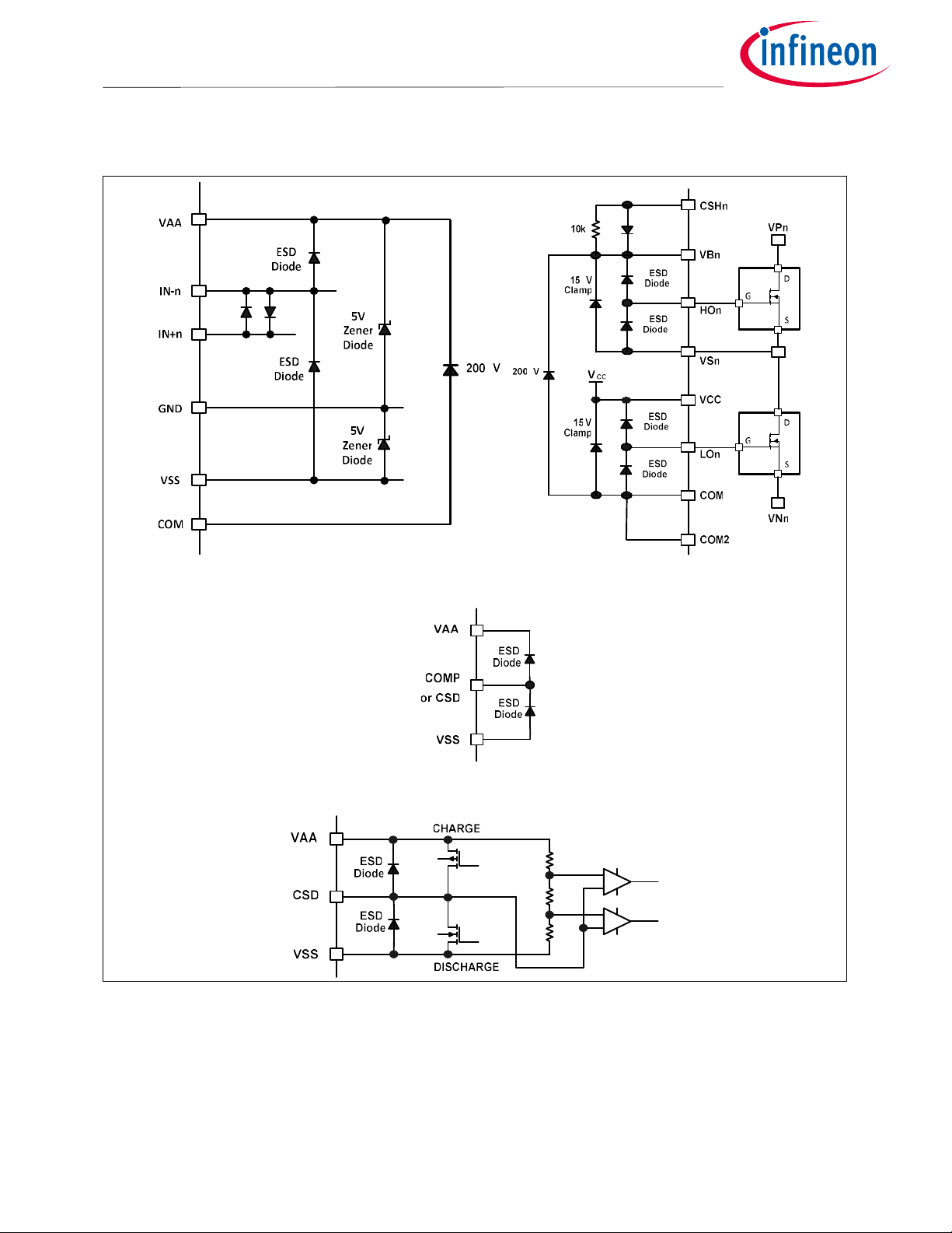
8 Input / Output pin equivalent circuit diagrams
,
Figure 29 Input/output pin equivalent circuit diagrams
Datasheet 33 of 59 V 2.0
9/24/2021
Page 34
MA
5332MS
Table of contents
Integrated Class D Amplifier
9 PWM Modulator Design
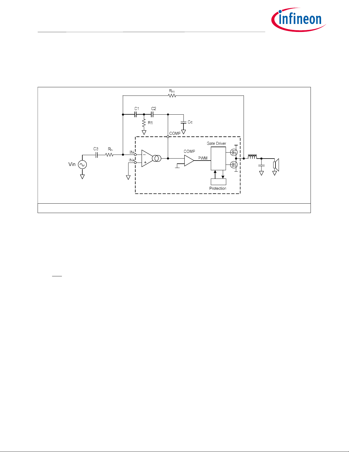
The open-access front-end configuration of MA5332MS enables many ways to implement a PWM modulator.
This section explains how PWM modulation works based on an example of a self-oscillating PWM modulator in
a typical application.
Figure 30 MA5332MS Typical Control Loop Design
9.1 Input Section
The audio input stage of MA5332MS forms an inverting error amplifier. The voltage gain of the amplifier, GV, is
determined by the ratio between input resistor RIN and feedback resistor RFB.
R
G
Since the feedback resistor RFB is part of an integrator time constant, which determines switching frequency,
changing the overall voltage gain by RIN is simpler and therefore recommended. Note that the input impedance
of the amplifier is equal to the input resistor RIN.
A DC blocking capacitor C3 should be connected in series with RIN to minimize the DC offset voltage on the output.
Due to potential distortion, a ceramic capacitor is not recommended. Minimizing the DC offset is essential to
minimize the audible noise during power-ON and -OFF.
The connection of the non-inverting input IN+ is a reference for the error amplifier, and thus is crucial for audio
performance. Connect IN+ to the signal reference ground in the system, which has the same potential as the
negative terminal of the speaker output.
FB
V
R
IN
Datasheet 34 of 59 V 2.0
9/24/2021
Page 35
MA
5332MS
Table of contents
Target Self
-
Oscillation
500 2.2 200 450 2.2 165
350 2.2 124 300 2.2 115
250 2.2 102 200 4.7 41.2 150 10 20.0
70 22 4.42
Integrated Class D Amplifier
9.2 Control Loop Design
The MA5332MS allows the user to choose from numerous methods of PWM modulator implementations. In this
section, all the explanations are based on a typical application circuit of a self-oscillating
9.3 PWM Frequency
Choosing the switching frequency entails making a trade-off between many aspects. At lower switching
frequency, conduction losses in the MOSFET stage increases due to higher inductor ripple current. The output
carrier leakage in the speaker output increases. At higher switching frequency, the efficiency degrades due to
higher switching losses. Higher switching frequency supports wider audio bandwidth. The inductor ripple
decreases yet core loss might increase. For these reasons, 400kHz is chosen for a typical design example.
Self-oscillating frequency has little influence from the bus voltage and input resistance RIN. Note that the
nature of a self-oscillating PWM is for the switching frequency to decrease as PWM modulation deviates from
idling.
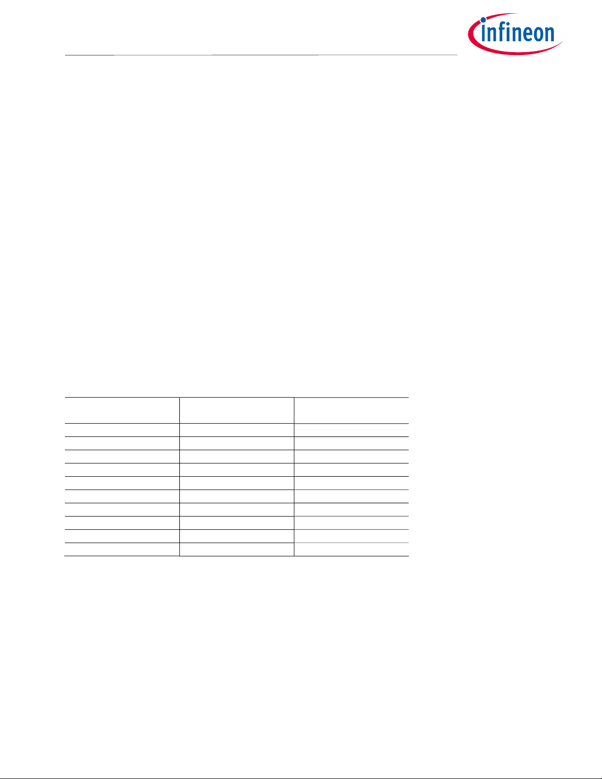
Table 10 summarizes suggested values of components for a given target self-oscillating frequency. The frontend operational transconductance amplifier (OTA) output has limited voltage and current compliances. This
set of component values ensures that OTA operates within its linear region for optimal THD+N performance. In
case the target frequency is somewhere in between the frequencies listed in Table 10, simply adjust the
frequency by tweaking R1.
Table 10 External Component Values vs. Self-Oscillation Frequency
Frequency (kHz) C1=C2 (nF) R1 (ohms)
400 2.2 141
100 10 14.0
Datasheet 35 of 59 V 2.0
9/24/2021
Page 36
MA
5332MS
Table of contents
Integrated Class D Amplifier
9.4 Clock Synchronization
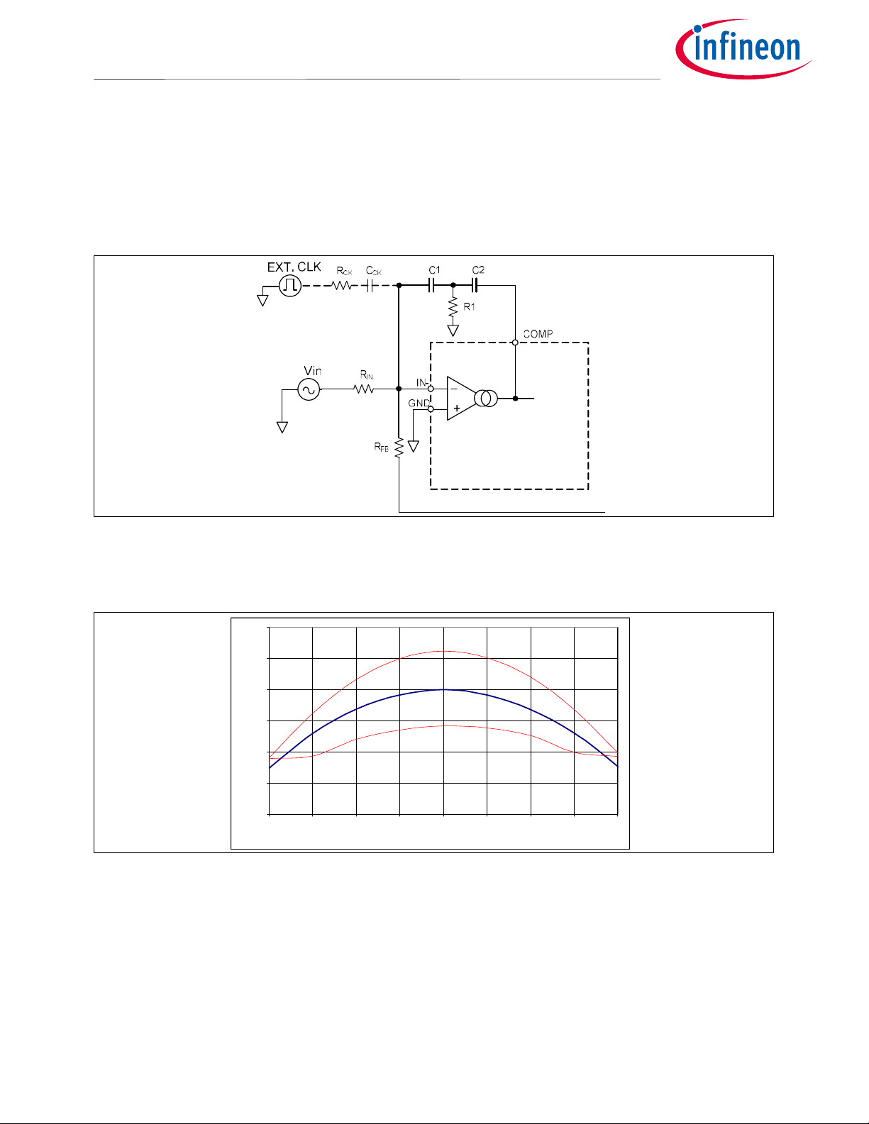
In the PWM control loop design example, the self-oscillating frequency can be set and synchronized to an external
clock. Through a set of resistors and a capacitor, the external clock injects periodic pulsating charges into the
integrator, forcing oscillation to lock up to the external clock frequency. A typical setup with 5 Vp-p 50% duty
clock signal uses RCK=22 kΩ and CCK=100 pF in Figure 31. To maximize audio performance, the self-running
frequency without clock injection should be 20 to 30% higher than the external clock frequency.
Figure 31 External Clock Synchronization
Figure 32 shows how a self-oscillating frequency locks up to an external clock frequency. A design of a 400 kHz
self-oscillating frequency synchronizes to an external clock whose frequency is within the red border lines.
600
500
400
300
200
Operating Frequency (kHz)
100
0
10% 20% 30% 40% 50% 60% 70% 80% 90%
Duty Cycle
Figure 32 Typical Lock Range to External Clock (RCK=22 kΩ and CCK=100 pF)
Datasheet 36 of 59 V 2.0
9/24/2021
Page 37
MA
5332MS
Table of contents
Integrated Class D Amplifier
9.5 Click Noise Elimination
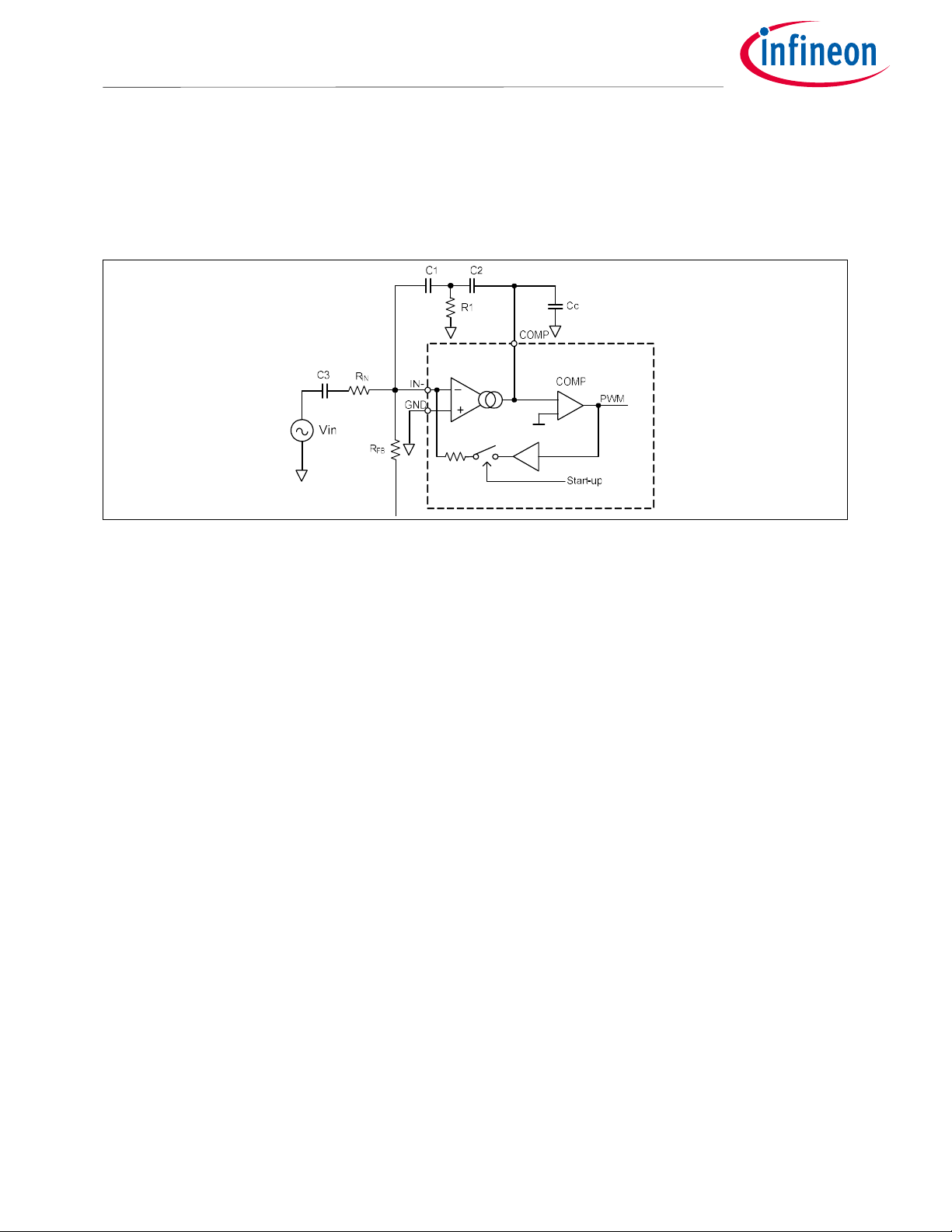
The MA5332MS has a unique feature that minimizes power-ON and -OFF audible click noise. When CSD is in
between Vth1 and Vth2 during start-up, an internal closed loop around the OTA enables an oscillation that
generates voltages at COMP and IN-, bringing them to steady-state values. It runs at around 1 MHz, independent
from the switching oscillation.
Figure 33 Audible Click Noise Elimination
As a result, all capacitive components connected to COMP and IN- pins, such as C1, C2, C3 and Cc in Figure 33,
are pre-charged to their steady-state values during the start-up sequence. This allows instant settling of closedloop PWM operation.
To utilize the click noise reduction function, the following conditions must be met.
1. CSD pin has slow enough ramp up from Vth1 to Vth2 such that the voltages in the capacitors can settle
to their target values.
2. High-side bootstrap power supply needs to be charged up prior to starting oscillation.
3. Audio input has to be zero.
4. For internal local loop to override external feedback during the startup period, DC offset at speaker
output prior to shutdown release has to satisfy the following condition.
Datasheet 37 of 59 V 2.0
9/24/2021
Page 38
MA
5332MS
Table of contents
Integrated Class D Amplifier
9.6 Differential Input
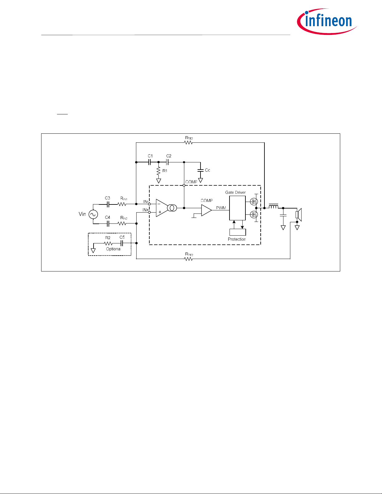
Figure 34 shows an example of a differential input configuration. This design is useful in a single supply
configuration. Use R
Voltage gain is given by a ratio between RIN and RFB.
R
G
FB
V
R
IN
IN1=RIN2
, R
FB1=RFB2
, C3=C4.
Figure 34 Differential Input
Although component values in the feedback network are balanced between inverting and non-inverting inputs,
the integration capacitor path in the non-inverting input creates unbalance at high frequencies, causing slightly
higher distortion compared to an unbalanced input configuration. To improve the THD degradations, place
optional RC network R2=R1 and C5=C1.
Datasheet 38 of 59 V 2.0
9/24/2021
Page 39
MA
5332MS
Table
of contents
Integrated Class D Amplifier
10 Operational Mode
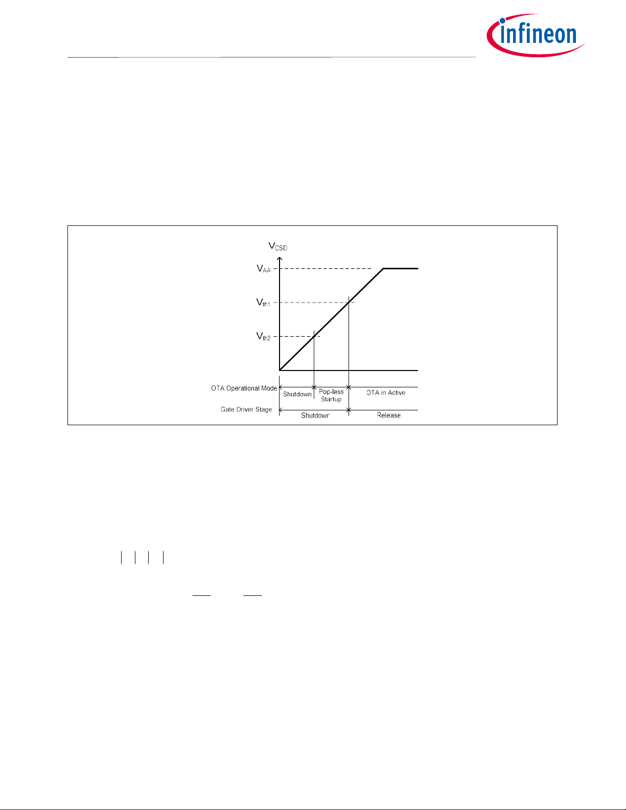
The CSD pin determines the operational mode of the MA5332MS as shown in Figure 35. The OTA has three
operational modes: shutdown, pop-less startup and normal operation; while the gate driver section has two
modes: shutdown and normal operation.
When V
MOSFETs are still in shutdown mode. The OTA is activated and starts local oscillation for pop-less start-up which
pre-biases all the capacitive components in the error amplifier. When V
operation mode and PWM operation starts.
< Vth2, the IC is in shutdown mode and the input OTA is cut off. When Vth2< V
CSD
>Vth1, the MA5332MS enters normal
CSD
< Vth1, the output
CSD
Figure 35 V
and Operational Mode
CSD
10.1 Self-oscillation Start-up Condition
The MA5332MS requires the following conditions in order for pop-less startup to work properly.
- All the control power supplies, VAA, VSS, VCC and VBS are above the under-voltage lockout
thresholds.
- CSD pin voltage is over Vth1 threshold.
-
- The duration CSD voltage transitioning from Vth2 to Vth1 is long enough to pre-charge input and
integration capacitors around OTA section.
ii
FBIN
Where
i
IN
V
IN
,
R
IN
i
FB
V
B
.
R
FB
Datasheet 39 of 59 V 2.0
9/24/2021
Page 40
MA
5332MS
Table of contents
Integrated Class D Amplifier
11 Protections
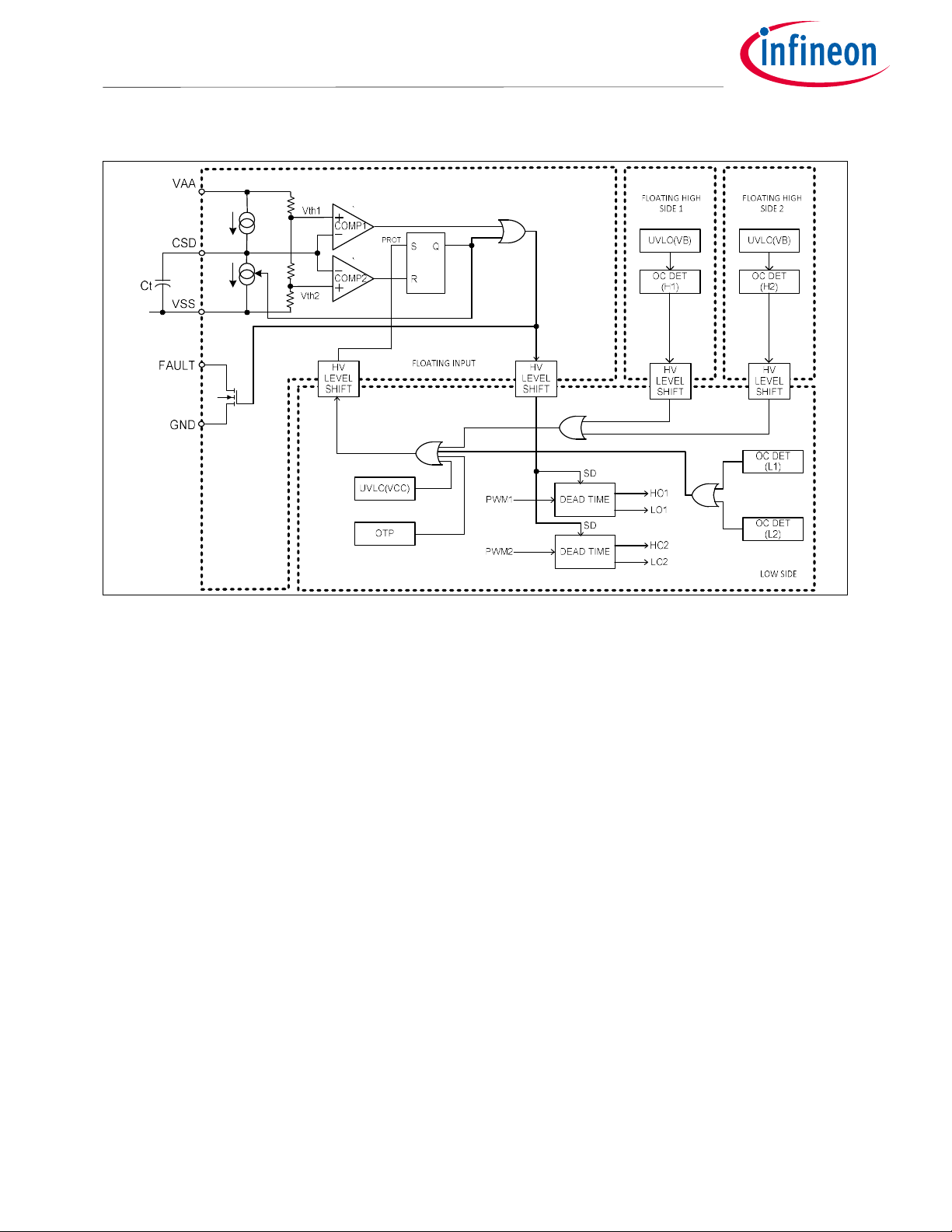
Figure 36 Protection Functional Block Diagram
The internal protection control block dictates the operational modes, normal or shutdown, using the input of the
CSD pin. In shutdown mode, the controller IC turns off internal power MOSFETs.
The CSD pin provides five functions.
1. Power up delay timer
2. Self-reset timer
3. Shutdown input
4. Latched protection configuration
5. Shutdown status output (host I/F)
The CSD pin cannot be paralleled with another MA5332MS directly.
The operating statuses of the protection features are shown in Table 11.
Datasheet 40 of 59 V 2.0
9/24/2021
Page 41
MA
5332MS
Table of contents
Event
CSD FAULT
UVCC, rising edge
Recycle
L until CSD>Vth1
UVCC, falling edge
n/a n/a
UVAA, rising edge
n/a L at VAA<UVAA
UVAA, falling edge
n/a L at V
AA<UVAA
UVBS, rising edge
n/a n/a
UVBS, falling edge
n/a n/a Over Current Protection
is reset
Held L until OCP
is reset
Clip Detection
n/a n/a
Protection
is reset
Held L
until OTP
is reset
Integrated Class D Amplifier
Table 11 Events and Actions of CSD and FAULT
Keep recycling until OCP
Over Temperature
Keep recycling until OTP
*CSD recycle: CSD pin voltage
discharges down to Vth2 and charges
back to VAA, if CSD pin is configured
as self reset protection.
11.1.1 Self-Reset Protection
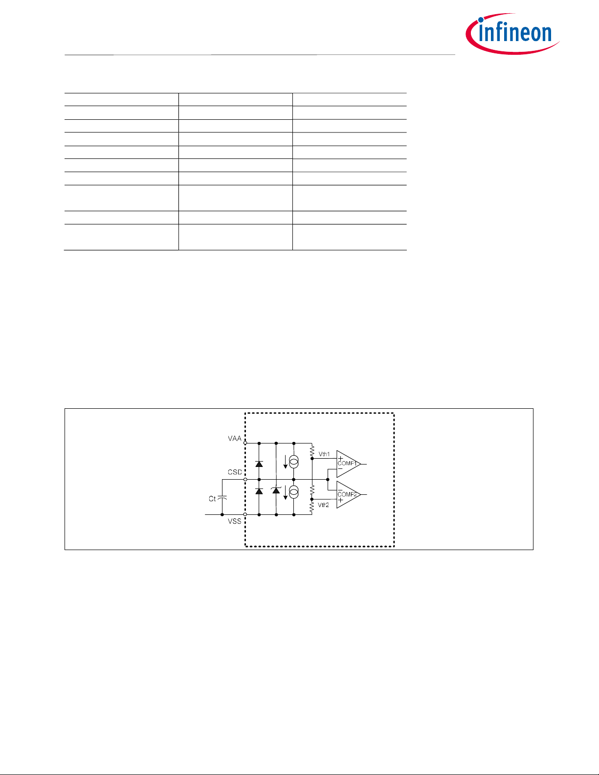
Attaching a capacitor between CSD and VSS configures the MA5332MS self-reset protection mode.
Upon an OCP event, the CSD pin discharges the external capacitor voltage V
to reset the internal shutdown latch. Then, the CSD pin begins to charge the external capacitor, Ct, in an attempt
to resume operation. Once the voltage of the CSD pin rises above the upper threshold, V
operation.
down to the lower threshold V
CSD
, the IC resumes normal
th1
th2
Figure 37 Self-Reset Protection Configuration
Datasheet 41 of 59 V 2.0
9/24/2021
Page 42
MA
5332MS
Table of contents
Integrated Class D Amplifier
11.1.2 Designing Ct
The external timing capacitor, Ct, programs self-reset timings: t
t
is the time that elapses from when the IC enters the shutdown mode to the time when the IC
RESET
resumes operation. t
should be long enough to avoid over heating the MOSFETs from the repetitive
RESET
RESET
and tSU.
sequence of shutting down and resuming operation during over-current conditions. In most
applications, the minimum recommended time for t
is 0.1 seconds.
RESET
tSU is the time between powering up the IC in shutdown mode to the moment the IC releases shutdown
to begin normal operation.
The Ct determines t
and tSU as following equations:
RESET
VCt
t
RESET
AA
1.1
[s]
I
CSD
VCt
t
SU
AA
7.0
[s]
I
CSD
where I
: the charge/discharge current at the CSD pin
CSD
VAA: the floating input supply voltage with respect to V
SS.
11.1.3 Shutdown Input
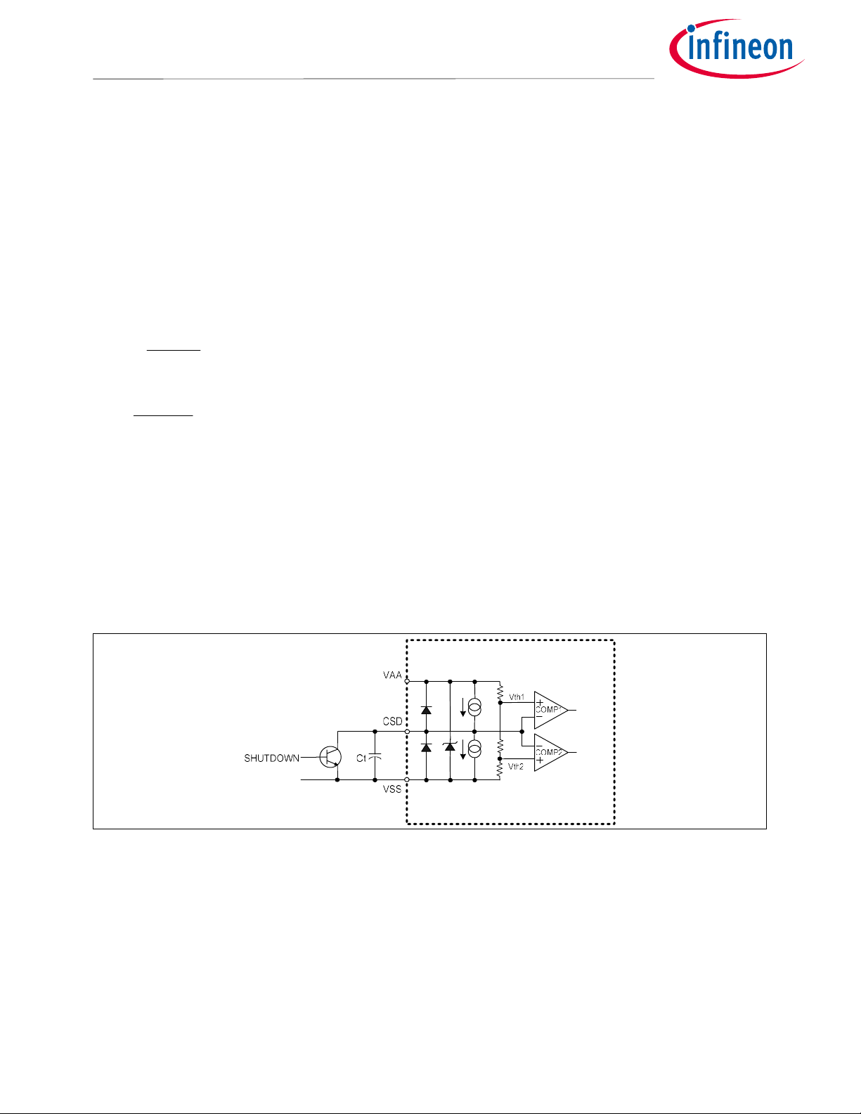
During normal operation, pulling the CSD pin below the upper threshold Vth1 forces the IC into shutdown mode.
Figure 38 shows how to add an external discharging path to shutdown the PWM.
Figure 38 Shutdown Input
Datasheet 42 of 59 V 2.0
9/24/2021
Page 43
MA
5332MS
Table of contents
Integrated Class D Amplifier
11.1.4 Latched Protection
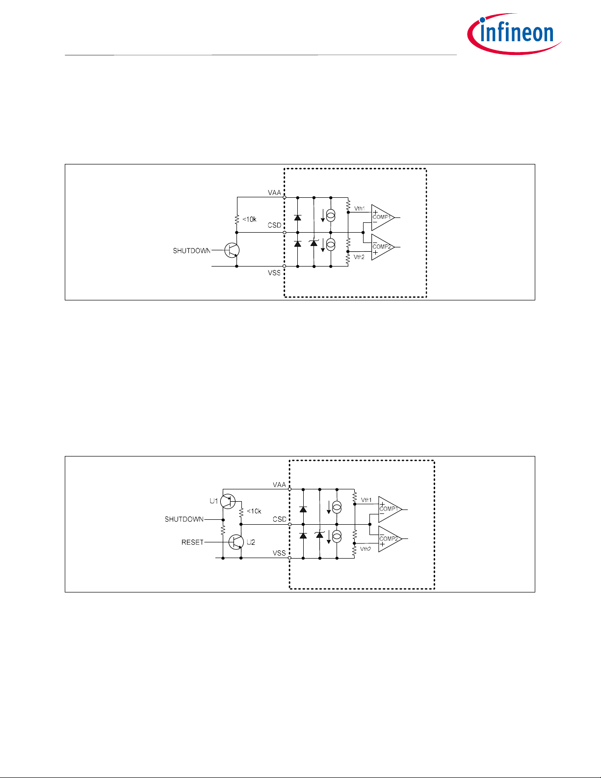
Connecting CSD to VAA through a 10 kΩ or less resistor configures latched protection mode. The internal
shutdown latch stays in shutdown mode after the overcurrent is detected. An external reset switch brings CSD
below the lower threshold Vth2 for a minimum of 200 ns and resets the latch. At first power-up, a reset signal to
the CSD pin is required to release the IC from shutdown mode.
Figure 39 Latched Protection with Reset Input
11.1.5 Interfacing with System Controller
The MA5332MS can communicate with an external system controller through a simple interfacing circuit shown
in Figure 40. A generic PNP transistor, U1, detects the sink current at the CSD pin during protection event and
outputs a shutdown flag signal to an external system controller. Another generic NPN transistor, U2, can then
reset the internal protection logic by pulling the CSD voltage below the lower threshold Vth2. After the first
power-up sequence, a reset signal to the CSD pin is required to release the IC from shutdown mode.
Figure 40 Interfacing CSD with System Controller
Datasheet 43 of 59 V 2.0
9/24/2021
Page 44
MA5332MS
Protections
Integrated Class D Amplifier
11.2 Over Current Protection (OCP)
The MA5332MS features over current protection to protect the internal power MOSFETs during abnormal load
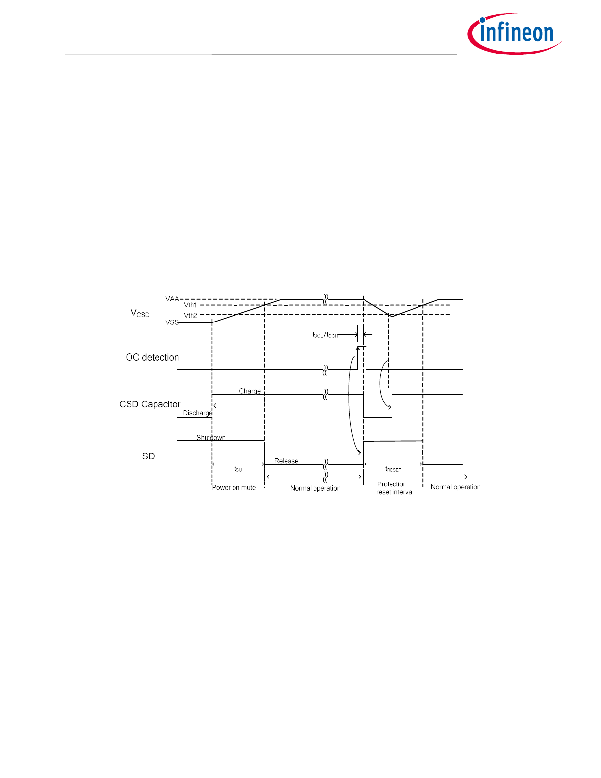
conditions. The control logic diagrams are in Figure 41. As soon as either the high-side or low-side current sensing
block detects over current, the following sequence will occur.
1. The shutdown latch flips its logic states from normal operational mode to shutdown mode.
2. Low-side and high-side MOSFETs go into an off state condition.
3. The CSD pin starts discharging the external capacitor Ct.
4. When voltage across Ct falls below the lower threshold Vth2, COMP2 resets the shutdown latch to normal
mode.
5. The CSD pin starts charging the external capacitor Ct.
6. When V
operation.
Figure 41 summarizes the above. As long as the over current condition exists, the IC will repeat the over current
protection sequence at a repetitive rate set by the CSD capacitor.
goes above the upper threshold Vth1, the logic on COMP1 toggles and the IC resumes
CSD
Figure 41 Overcurrent Protection Timing Chart
Datasheet 44 of 59 V 2.0
9/24/2021
Page 45

MA5332MS
Protections
Integrated Class D Amplifier
11.3 Over Temperature Protection (OTP)
If the junction temperature TJ of the controller IC exceeds the on-chip thermal shutdown threshold, TSD, the onchip over temperature protection shuts down the PWM.
11.4 Under Voltage Protection (UVP)
In order to prevent a partial on-state of the internal MOSFET, under-voltage protection monitors the low side and
high side gate bias supplies, VCC and VB. When VCC is below UVLO, both high and low side MOSFETs are turned
off. When the high side supply VBS is below the UVLO threshold, the high side output is disabled, while the low
side works normally.
Datasheet 45 of 59 V 2.0
9/24/2021
Page 46
MA5332MS
Status Output
Integrated Class D Amplifier
12 Status Output
12.1 Fault Output
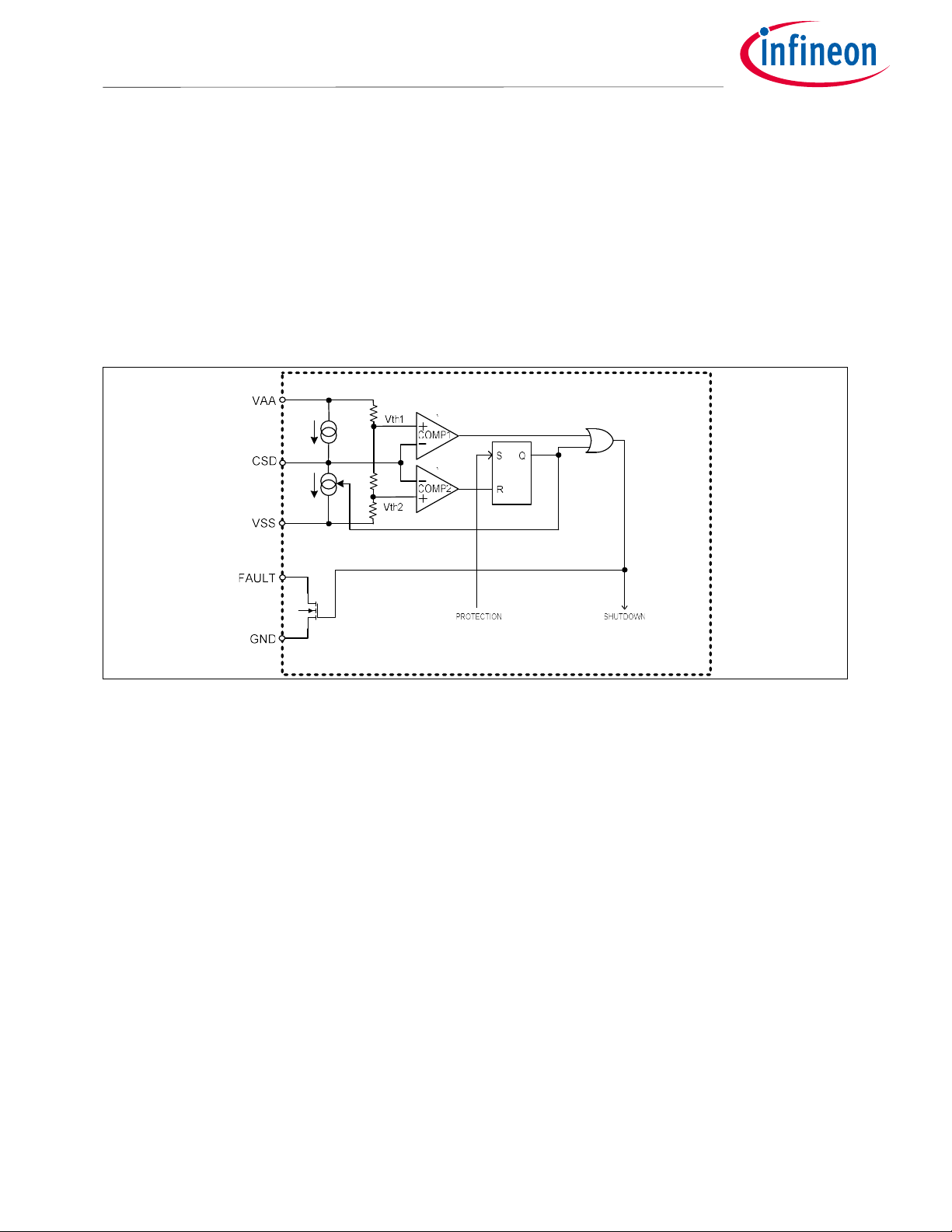
FAULT output is an open drain output referenced to GND to report whether the MA5332MS is in shutdown mode
or in normal operating mode. If the FAULT pin is open, the MA5332MS is in normal operation mode, i.e. the
output MOSFETs are active. The following conditions trigger shutdown internally and pulls the FAULT pin down
to GND.
Over Current Protection
Over Temperature Protection
Shutdown mode from CSD pin voltage
Figure 42 Fault Output
Datasheet 46 of 59 V 2.0
9/24/2021
Page 47
MA5332MS
Status Output
Integrated Class D Amplifier
12.2 CLIP Output
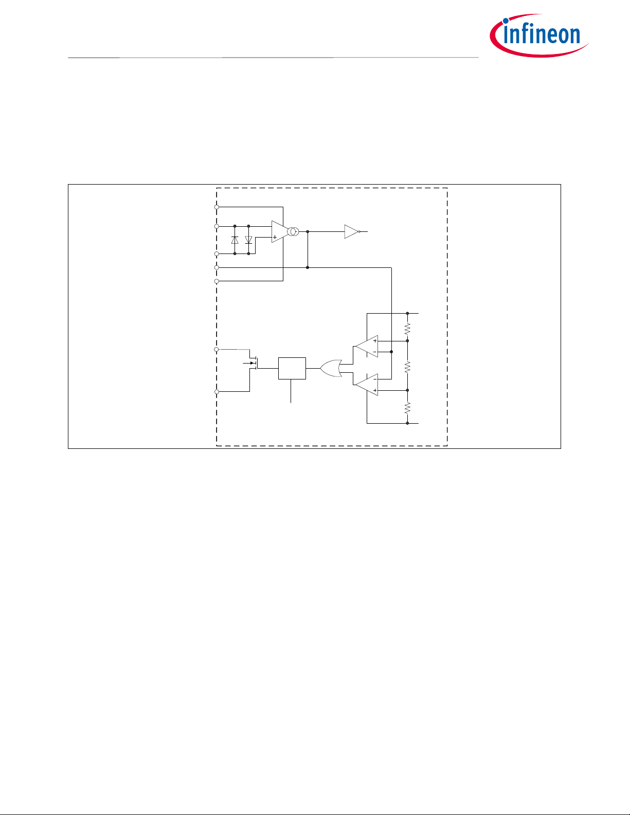
When the output of the amplifier loses track of an expected target value, the amplifier enters into clipping
condition.
The CLIP detection block monitors the COMP pin voltage with a window comparator. The CLIP pin is pulled to
GND when a clipping condition is detected. The detection thresholds in the COMP pin are at 10% and 90% of
VAA-VSS. The CLIP outputs are disabled in shutdown mode.
VAA
Figure 43 CLIP Detection
IN-
IN+
COMP
VSS
CLIP1
GND
OTA
PGEN
SD
PWM
VAA
R
R
R
VSS
Datasheet 47 of 59 V 2.0
9/24/2021
Page 48
MA5332MS
Power Supply Design
Integrated Class D Amplifier
13 Power Supply Design
13.1 Supplying VAA and VSS
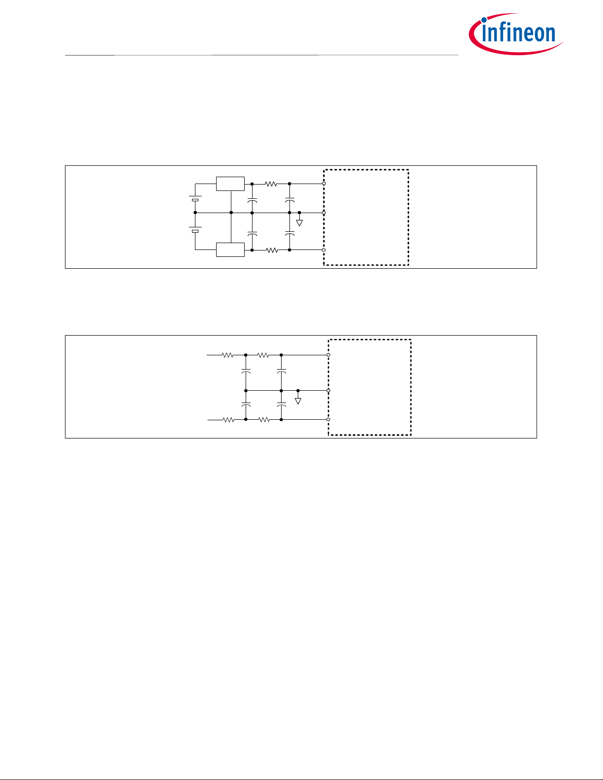
VAA and VSS are supply voltages to the front-end of the analog section, hence are noise sensitive. For best
audio performance, use regulated power supplies for VAA and VSS.
7805
7905
10
2.2µF
2.2µF
10
Figure 44 Supplying VAA and VSS with External Voltage Regulators
VAA
GND
VSS
MA53xx
When switched-mode regulators are used as supply voltages for VAA and VSS, place a two-stage R-C noise filter
in the supply lines as shown in Figure 45.
+5V
-5V
10
10µF
10µF
10
10
2.2µF
2.2µF
10
VAA
GND
VSS
MA53xx
Figure 45 Supplying VAA and VSS from Switched Mode Power Supply
13.2 Supplying VCC and VB
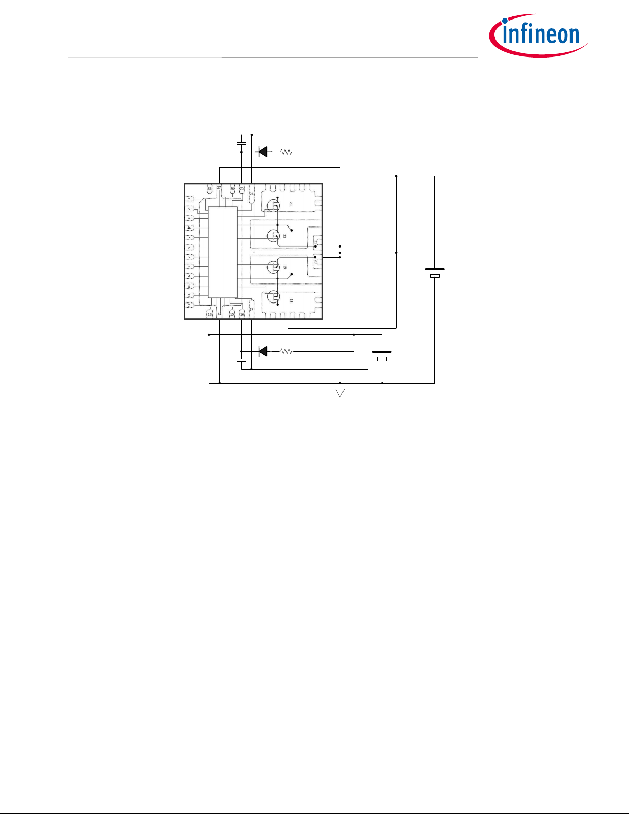
Figure 46 shows the recommended power supply configuration for gate driver power supplies. The gate driver
stage has three power supply inputs:
1. VCC-COM: low side gate drive supply
2. VB1-VS1: CH1 high side gate drive supply
3. VB2-VS2: CH2 high side gate drive supply
The low-side power supply, VCC, feeds the internal gate drive logic and low side gate driver. In order to protect
VCC from switching noise generated by the VS node, it is recommended to insert a few ohms of R
bootstrap charging path.
VBS
in the
The high-side driver requires a floating supply VBn referenced to the respective switching node VSn where the
source of the output MOSFET is connected. A charge pump method (floating bootstrap power supply)
eliminates the need for a floating power supply and thus is used in the typical application circuit. The floating
bootstrap power supply charges the bootstrap capacitor C
low-side MOSFET ON period. When the high-side MOSFET is ON, the diode cuts off and floats the VBS supply. CBS
retains its VB supply voltage for the rest of the high-side ON duration.
Datasheet 48 of 59 V 2.0
9/24/2021
from the low-side power supply VCC during the
BS
Page 49
MA5332MS
Power Supply Design
Integrated Class D Amplifier
fQIII 2
PWMGQBSQCCVCC
/per channel
Recommend to have minimum 20% design margin for Ivcc.
R
VPN2
4.7
VP2
VP1
CLIP
COMP2
IN-2
IN+2
GND
VSS
VAA
IN+1
IN-1
COMP1
CSD
FAULT
C
VBS2
10uF
CSH2
COM
VB2
VS2
COM
VCC
CSH1
VB1
VS1
VS2
VN2
VN1
VS1
C
BP
100nF
Vbus
C
VCC
1uF
C
VBS1
10uF
R
VPN1
4.7
VCC
Figure 46 Recommended Power Supply Configurations for Output Stage
13.2.1 Choosing Bootstrap Capacitance
Often MA5332MS uses hard clipping condition. The continuous high-side ON duration could continue as long as
half of the lowest audio frequency, tens of milliseconds. A typical application uses a 22 uF CBS to support low
audio frequency clipping. A ceramic capacitor (X7R, X5R or X5S type) or aluminum electrolytic capacitor with 25
V or higher voltage rating is recommended.
13.2.2 Choosing Bootstrap Diode
Use a bootstrap charging diode with voltage rating of 1.5 x the maximum bus voltage. In order to charge the
bootstrap capacitor in a very short low-side ON period with a high PWM modulation ratio, a fast recovery diode
type (trr<50ns) is recommended.
13.2.3 Charging VBS Prior to Start
For proper start-up, pre-charging the bootstrap supply VBS prior to PWM start-up is necessary for self-oscillating
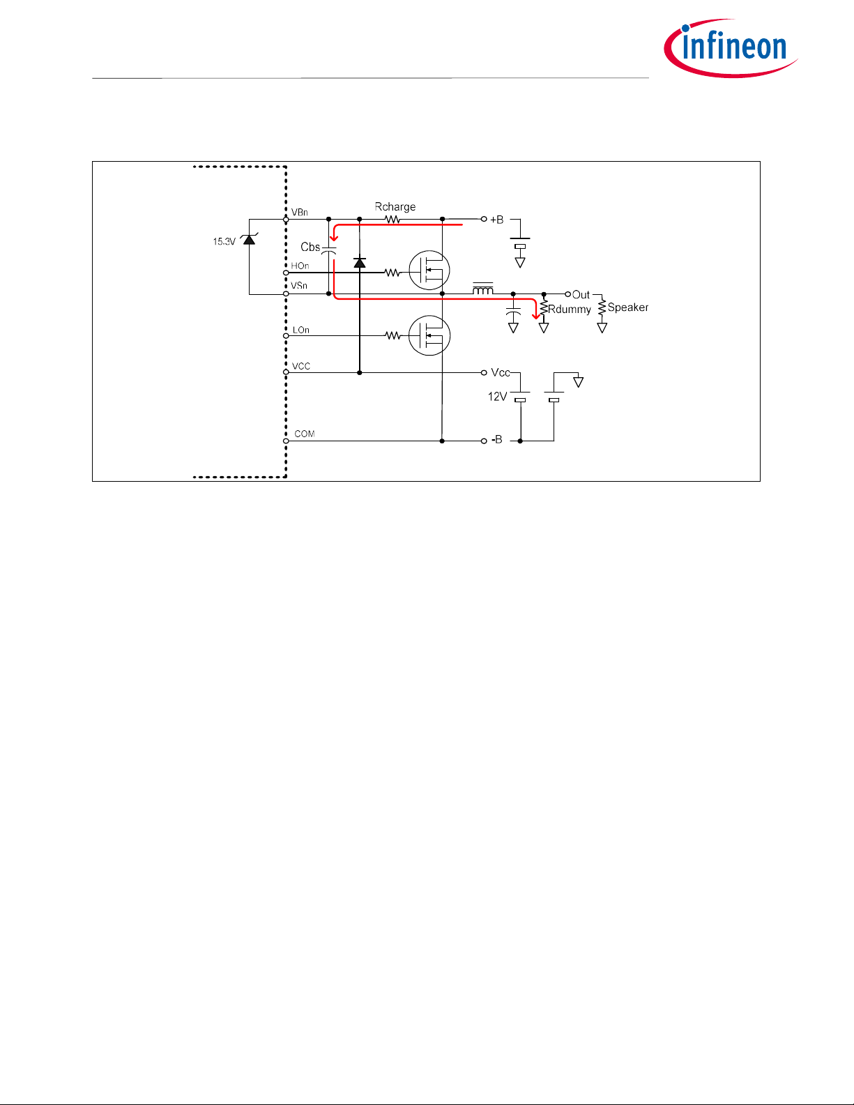
PWM modulator topologies. A charging resistor, R
charges CBS prior to switching start as shown in Figure 47. The minimum resistance of R
maximum PWM modulation index of the system. When the high-side MOSFET is on, R
power supply together with the quiescent current, I
continuous high-side on time.
The maximum resistance of R
Datasheet 49 of 59 V 2.0
9/24/2021
inserted between the positive supply bus and VB,
CHARGE,
is limited by the
CHARGE
drains the bootstrap
CHARGE
so it reduces the holding time, resulting in maximum
QBS,
is limited by the current charge capability of the resistor during startup.
CHARGE
Page 50
MA5332MS
Power Supply Design
Integrated Class D Amplifier
Pre-charging current flows into the speaker load. In order to startup without the load connected, a dummy load
R
in parallel with the speaker output provides a pre-charging current path.
dummy
Figure 47 Bootstrap Supply Pre-Charging
Datasheet 50 of 59 V 2.0
9/24/2021
Page 51
MA5332MS
Power Supply Design
Integrated Class D Amplifier
13.3 Power Supply Sequence
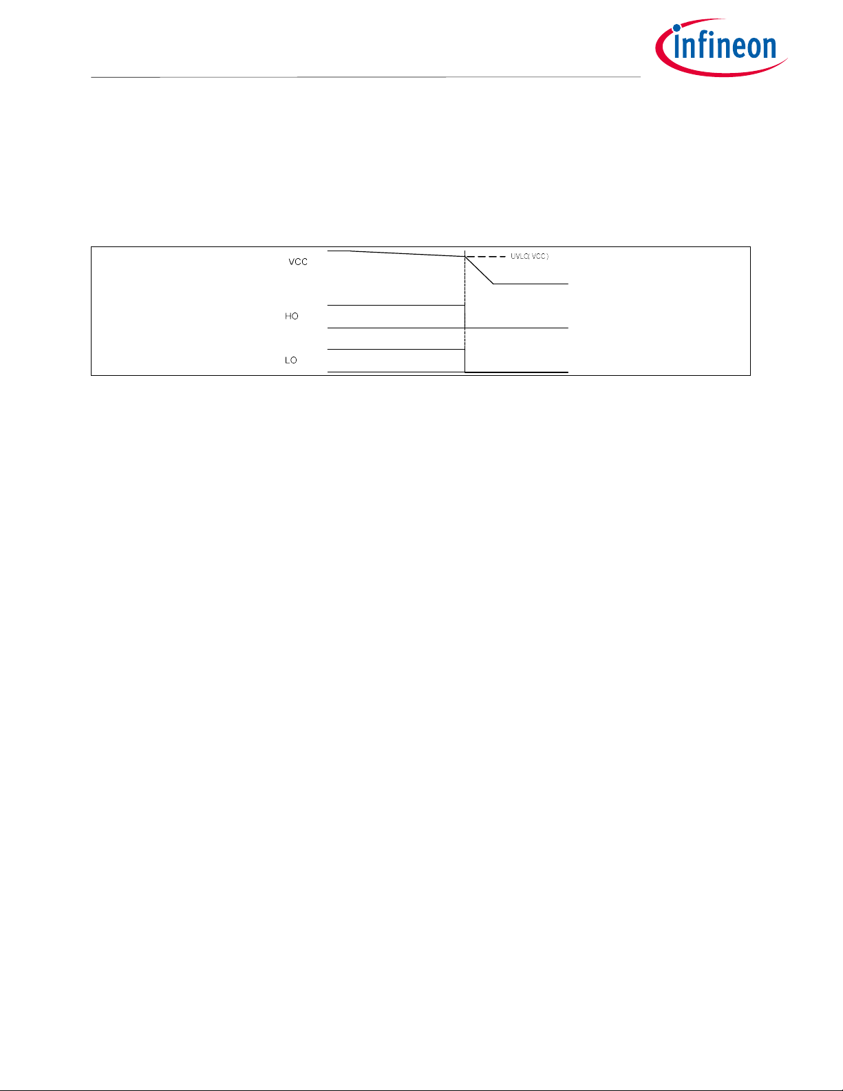
The protection control block in the MA5332MS monitors the status of VAA and VCC to ensure that both voltage
supplies are above their respective UVLO (under voltage lockout) thresholds before starting normal operation. If
either VAA or VCC is below the under voltage threshold, the output MOSFETs are disabled in shutdown mode until
both VAA and VCC rise above their voltage thresholds. As soon as VAA or VCC falls below its UVLO threshold, protection
logic in the MA5332MS turns off high-side and low-side.
Figure 48 MA5332MS UVLO Timing Chart
Datasheet 51 of 59 V 2.0
9/24/2021
Page 52
MA5332MS
Package details
Integrated Class D Amplifier
14 Package details
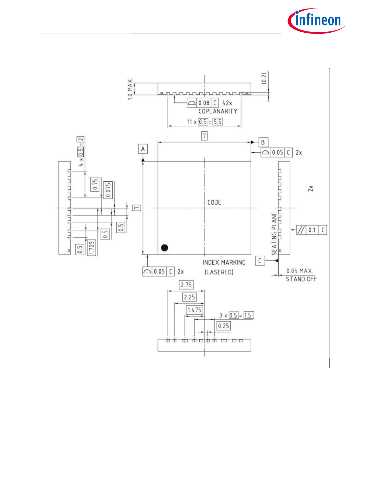
Figure 49 Package details
Datasheet 52 of 59 V 2.0
9/24/2021
Page 53
MA5332MS
Package details
Integrated Class D Amplifier
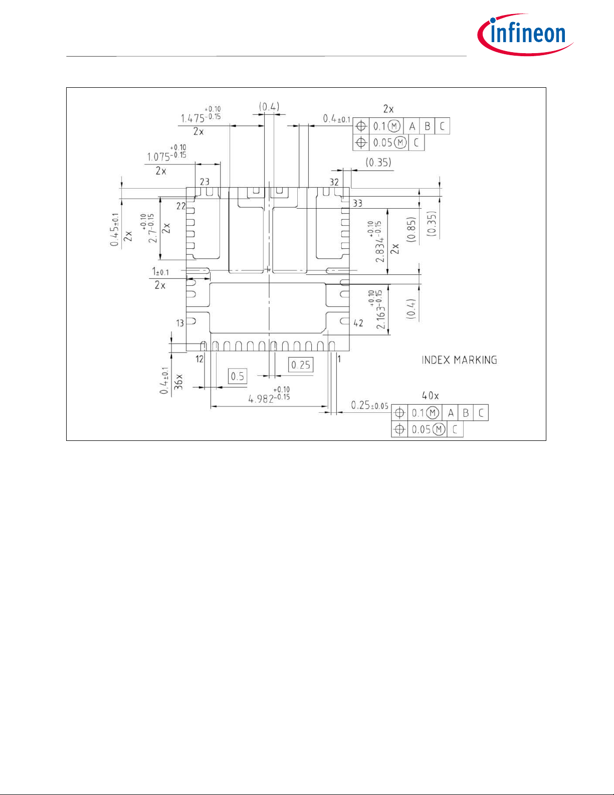
Figure 50 Package details; Bottom metallization detail view
Datasheet 53 of 59 V 2.0
9/24/2021
Page 54
MA5332MS
Package details
Integrated Class D Amplifier
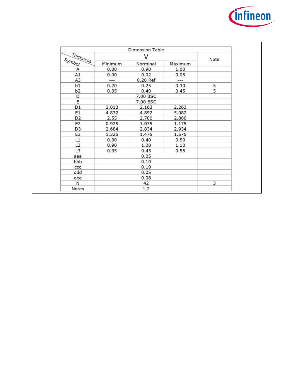
Figure 51 Dimension table
Datasheet 54 of 59 V 2.0
9/24/2021
Page 55
MA5332MS
Board mounting, part marking, and ordering information
Integrated Class D Amplifier
15 Board mounting, part marking, and ordering information
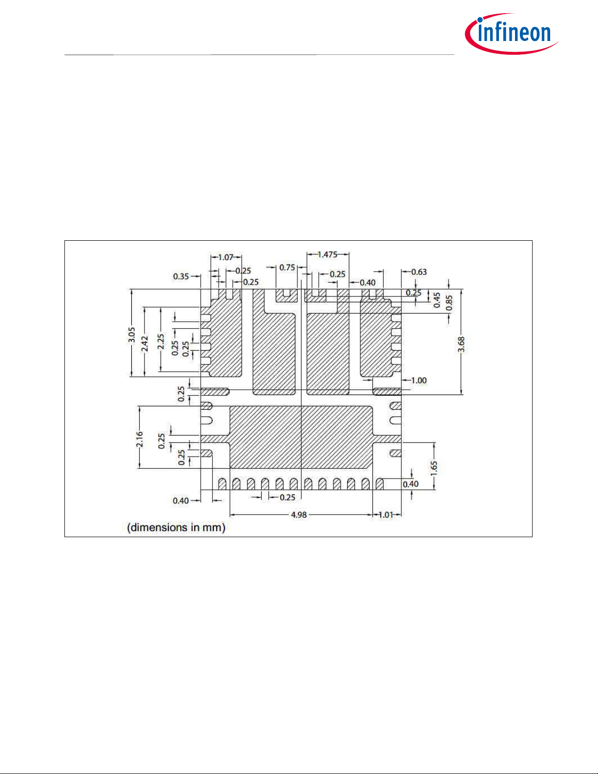
Reliability of products in the PQFN package is subject to the board mounting process. The Soldering
process is critical. Refer to Application Note AN-1170 Audio IC Board Mounting Application Note for
specific footprint design and soldering methods.
Device outline
Figure 52 shows the outline for these devices. The relative pad positions are controlled to an accuracy of
±0.050mm. For full dimensions and tolerances of each device, and to find out its size and outline, refer to the
relevant product data sheet and package outline drawing.
Figure 52 42-lead 7x7 device outline
Datasheet 55 of 59 V 2.0
9/24/2021
Page 56
MA5332MS
Board mounting, part marking, and ordering information
Integrated Class D Amplifier
Substrate/PCB layout
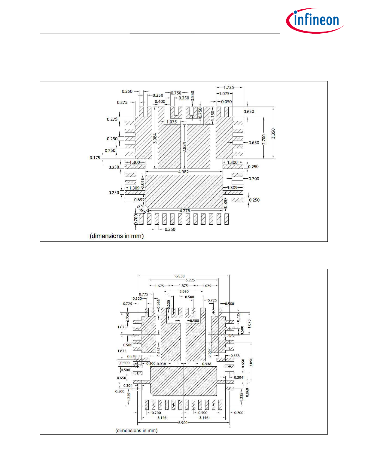
Evaluations have shown that the best overall performance is achieved using the substrate/PCB layout shown in
Figure 53 and Figure 54
Figure 53 42-lead 7x7 substrate /PCB layout_1
Figure 54 42-lead 7x7 substrate /PCB layout_2
Datasheet 56 of 59 V 2.0
9/24/2021
Page 57
MA5332MS
Board mounti
ng, part marking, and ordering information
Integrated Class D Amplifier
Stencil Design
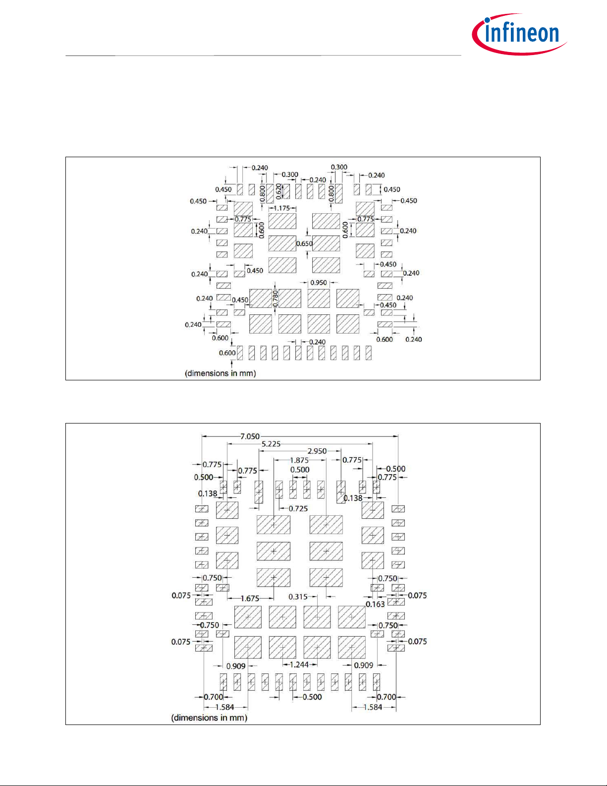
Evaluations have shown that the best overall performance is achieved using the stencil design shown in
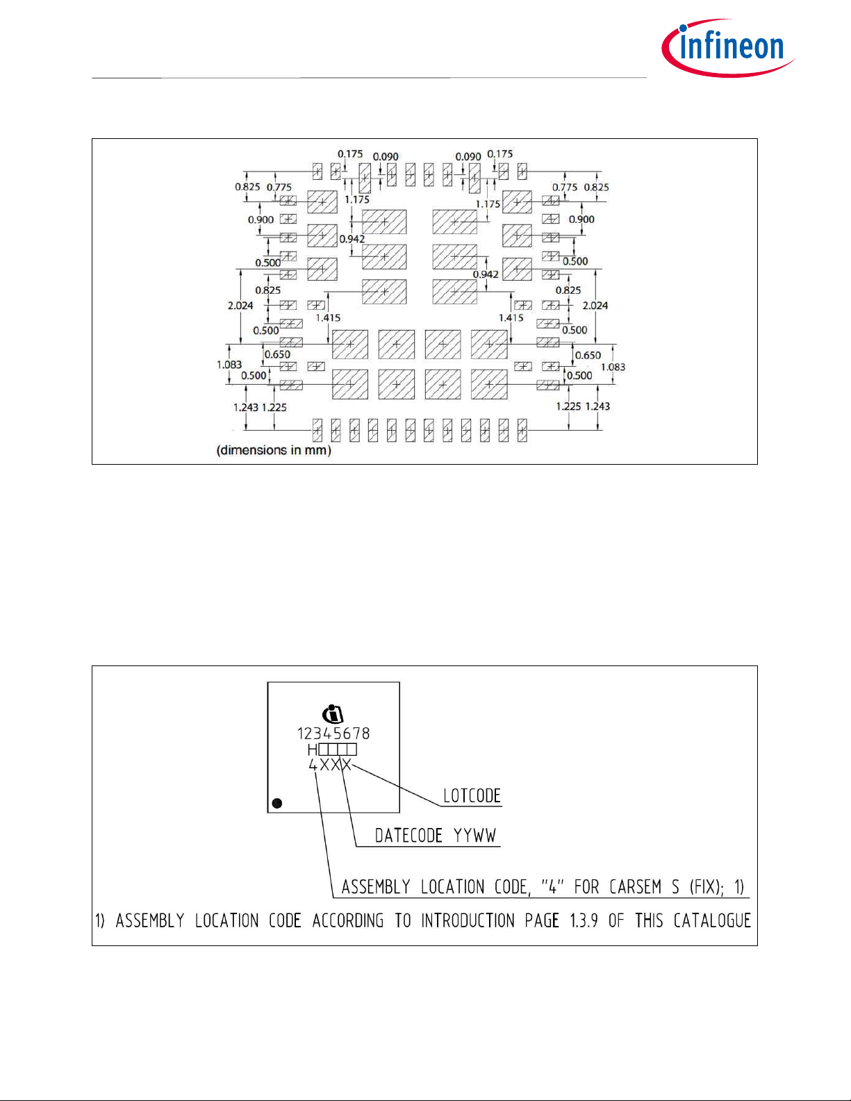
Figure 55-58.
Figure 55 42-lead 7x7 stencil design_1
Datasheet 57 of 59 V 2.0
9/24/2021
Page 58
MA5332MS
Board mounting, part marking, and ordering information
Integrated Class D Amplifier
Figure 56 42-lead 7x7 stencil design_2
Figure 57 42-lead 7x7 stencil design_3
Note: This design is for a stencil thickness of 0.127mm (0.005"). The reduction should be adjusted for
stencils of other thicknesses. All soldering conditions are necessary to ensure reliability. More
details please refer to Application Note AN-1170 Audio Power Quad Flat No-Lead (PQFN) Board
Mounting Application
Part marking
Figure 58 Part marking
Datasheet 58 of 59 V 2.0
9/24/2021
Page 59
MA5332MS
Board mounting, part marking, and ordering informati
on
Integrated Class D Amplifier
Ordering information
Base part number Package type
MA5332MS 7x7mm PG- IQFN-42 Tape and Reel 3000 MA5332MS
Standard pack
Complete part number
Form Quantity
Datasheet 59 of 59 V 2.0
9/24/2021
Page 60

100VIntegratedClassDAmplifier
MA5332MS
RevisionHistory
MA5332MS
Revision:2021-09-25,Rev.2.0
Previous Revision
Revision Date Subjects (major changes since last revision)
2.0
Trademarks
Allreferencedproductorservicenamesandtrademarksarethepropertyoftheirrespectiveowners.
WeListentoYourComments
Anyinformationwithinthisdocumentthatyoufeeliswrong,unclearormissingatall?Yourfeedbackwillhelpustocontinuously
improvethequalityofthisdocument.Pleasesendyourproposal(includingareferencetothisdocument)to:
Publishedby
InfineonTechnologiesAG
81726München,Germany
©2020InfineonTechnologiesAG
AllRightsReserved.
2021-09-25
Release of final version
LegalDisclaimer
Theinformationgiveninthisdocumentshallinnoeventberegardedasaguaranteeofconditionsorcharacteristics
(“Beschaffenheitsgarantie”).
Withrespecttoanyexamples,hintsoranytypicalvaluesstatedhereinand/oranyinformationregardingtheapplicationofthe
product,InfineonTechnologiesherebydisclaimsanyandallwarrantiesandliabilitiesofanykind,includingwithoutlimitation
warrantiesofnon-infringementofintellectualpropertyrightsofanythirdparty.
Inaddition,anyinformationgiveninthisdocumentissubjecttocustomer’scompliancewithitsobligationsstatedinthis
documentandanyapplicablelegalrequirements,normsandstandardsconcerningcustomer’sproductsandanyuseofthe
productofInfineonTechnologiesincustomer’sapplications.
Thedatacontainedinthisdocumentisexclusivelyintendedfortechnicallytrainedstaff.Itistheresponsibilityofcustomer’s
technicaldepartmentstoevaluatethesuitabilityoftheproductfortheintendedapplicationandthecompletenessoftheproduct
informationgiveninthisdocumentwithrespecttosuchapplication.
Information
Forfurtherinformationontechnology,deliverytermsandconditionsandpricespleasecontactyournearestInfineon
TechnologiesOffice(www.infineon.com).
Warnings
Duetotechnicalrequirements,componentsmaycontaindangeroussubstances.Forinformationonthetypesinquestion,
pleasecontactthenearestInfineonTechnologiesOffice.
TheInfineonTechnologiescomponentdescribedinthisDataSheetmaybeusedinlife-supportdevicesorsystemsand/or
automotive,aviationandaerospaceapplicationsorsystemsonlywiththeexpresswrittenapprovalofInfineonTechnologies,ifa
failureofsuchcomponentscanreasonablybeexpectedtocausethefailureofthatlife-support,automotive,aviationand
aerospacedeviceorsystemortoaffectthesafetyoreffectivenessofthatdeviceorsystem.Lifesupportdevicesorsystemsare
intendedtobeimplantedinthehumanbodyortosupportand/ormaintainandsustainand/orprotecthumanlife.Iftheyfail,itis
reasonabletoassumethatthehealthoftheuserorotherpersonsmaybeendangered.
60
Rev.2.0,2021-09-25
 Loading...