

Page 1
MA08509D
10W Power Amplifier Die Preliminary Release
(8.0-11 GHz)
FEATURES
DD
V
• Broadband Perform anc e
• 32% Typical Power Added Efficiency
• 50 Ω Input/Output Impedance
• Self-Aligned MSAG® MESFET Process
RF
IN
GG
V
Description Maximum Ratings (T
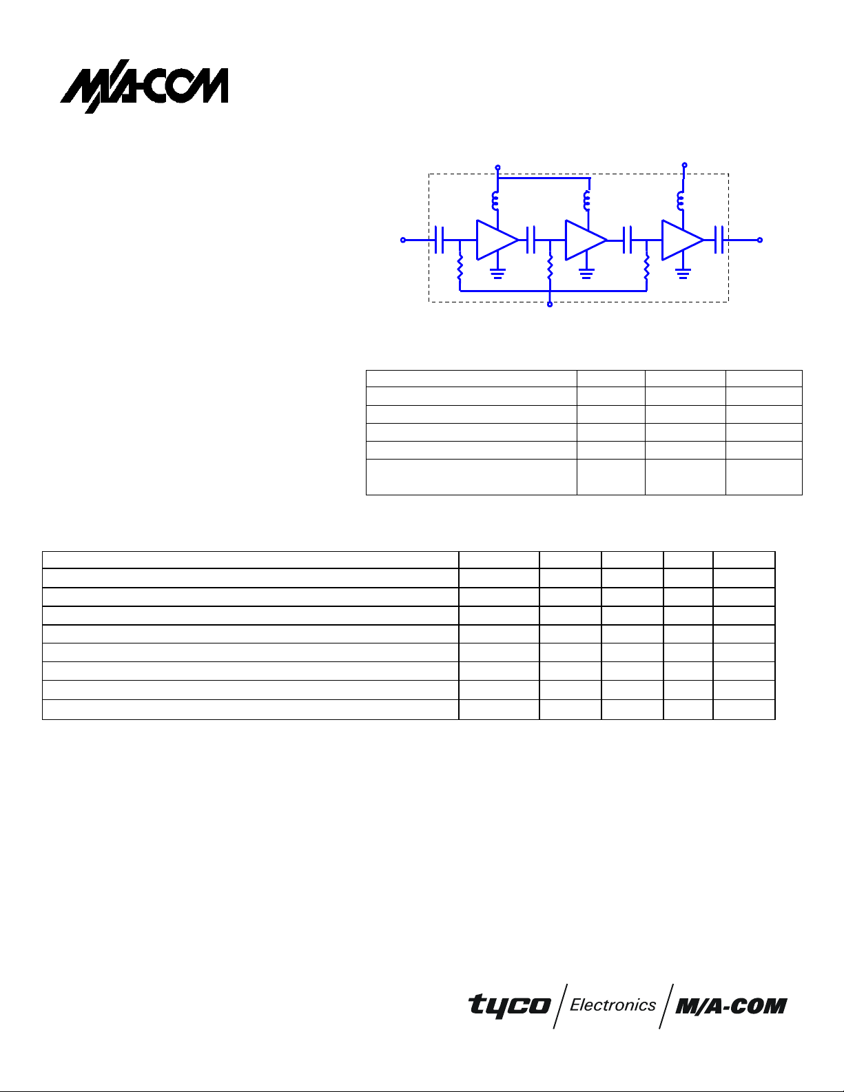
The MA08509D is a three stage MMIC power
amplifier fabricated using M/A-COM’s mature
GaAs Self-Aligned MSAG
®
MESFET Process.
This product is fully matched to 50 ohms on
both the input and the output.
ELECTRICAL CHARACTERISTICS V
Characteristic Symbol Min Typ Max Unit
Frequency
Output Power, saturated P
Power Gain, saturated G
Gain Flatness Over Frequency @ Pin = 18 dBm
Power Added Efficiency (P
OUT=PSAT
Return Loss S11 -6 -4 dB
Harmonics
Output Stage Thermal Resistance @ Pin = 18 dBm Rth 5.4
) PAE 25 32 %
DD
Rating Symbol Value Unit
DC Drain Supply Voltage VDD 12
DC Gate Supply Voltage VGG -6 Vdc
RF Input Power
Junction Temperature
Storage Temperature T
= 10.0 V, V
= -4 V, PIN = 18 dBm, TA = 25 °C
GG
ƒ
39.0 40 41.5 dBm
SAT
20 22 dB
SAT
- +/- 1.0 dB
, 3ƒο
2ƒ
ο
DD
V
OUT
RF
= 25 °C unless otherwise noted)
A
Vdc
PIN 500 mW
TJ 150 °C
-40 to
STG
°C
+85
8.0 - 11.0 GHz
-30 dBc
°C/W
Specifications subject to change without notice.
North America: Tel. (800)366-2266, Fax (800)618-8883
Asia/Pacific: Tel. +81-44-844-8296, Fax +81-44-844-8298
Europe: Tel. +44 (1344) 869 595, Fax +44 (1344) 300 020
Visit www.macom.com for additional data sheets and product information
902179 D
Page 2
10W Power Amplifier Die (8-11 GHz) MA08509D
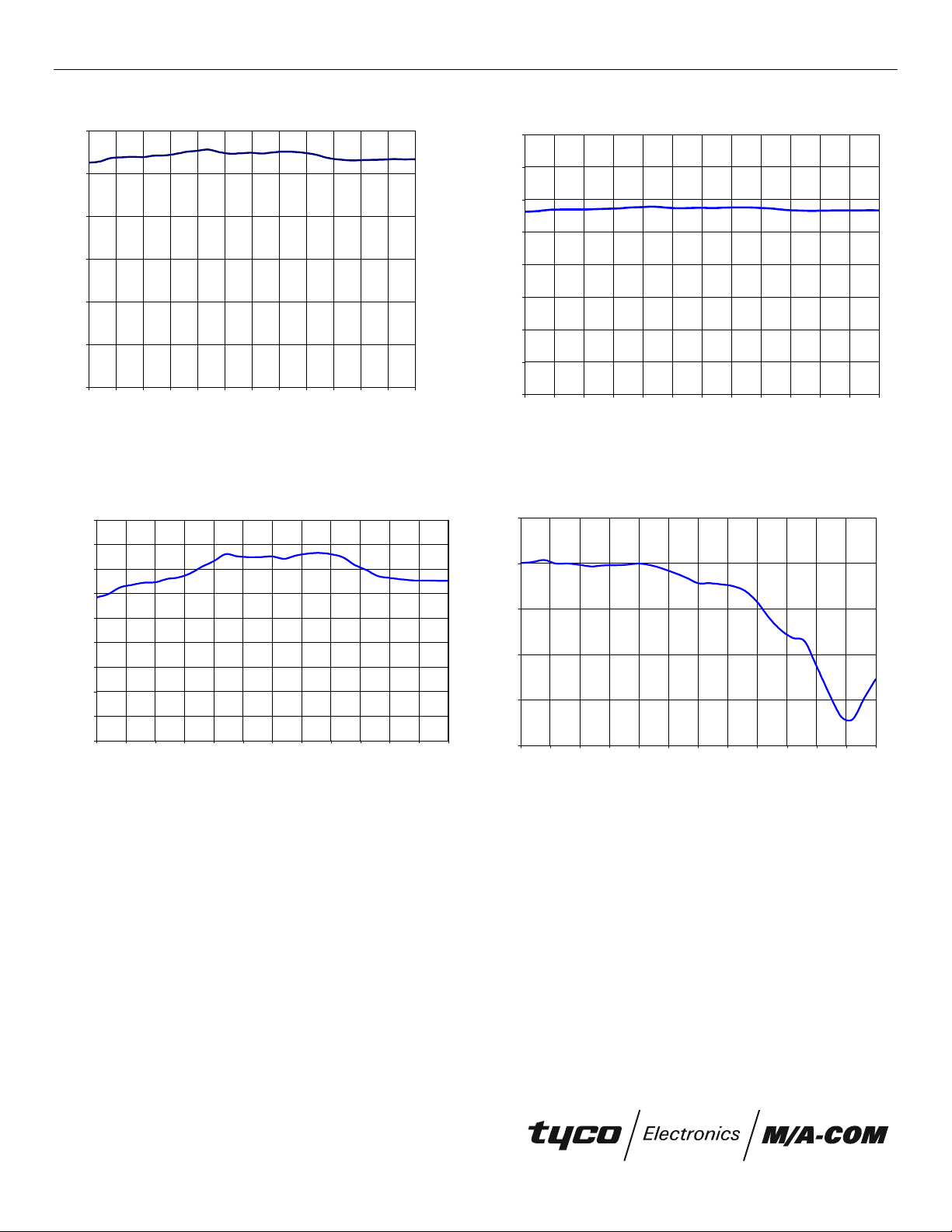
TYPICAL CHARACTERISTICS (V
42
= 10 V, VGG = -4 V, PIN = 18 dBm)
DD
32
40
38
36
Pout (dBm)
34
32
30
8 8.25 8.5 8.75 9 9.25 9.5 9.75 10 10.25 10.5 10.75 11
Frequency (GHz)
28
24
20
16
Gain (dB)
12
8
4
0
8 8.25 8.5 8.75 9 9.25 9.5 9.75 10 10.25 10.5 10.75 11
Frequency (GHz)
Figure 1. Output Power vs. Frequency Figure 2. Gain vs. Frequency
45
40
35
30
25
20
PAE (%)
15
10
5
0
8 8.25 8.5 8.75 9 9.25 9.5 9.75 10 10.25 10.5 10.75 11
Frequency (GHz)
0
-5
-10
-15
Return Loss(dB)
-20
-25
8 8.25 8.5 8.75 9 9.25 9.5 9.75 10 10.25 10.5 10.75 11
Frequency (GHz)
Figure 3. Power Added Efficiency vs. Frequency Figure 4. Input Return Loss vs. Frequency
Specifications subject to change without notice.
North America: Tel. (800)366-2266, Fax (800)618-8883
Asia/Pacific: Tel. +81-44-844-8296, Fax +81-44-844-8298
Europe: Tel. +44 (1344) 869 595, Fax +44 (1344) 300 020
Visit www.macom.com for additional data sheets and product information
902179 D
Page 3

10W Power Amplifier Die (8-11 GHz) MA08509D
APPLICATION INFORMATION
F
µ
F
µ
0.1
RF IN
F
µ
0.1
50 Ω
VGG
5000 pF
5000 pF
VGG
100 pF
100 pF
F
µ
0.1
VDD
VDD
5000 pF
0.1
VDD
50
VDD
F
µ
0.1
F
µ
0.1
5000 pF
5000 pF
RF OUT
Ω
5000 pF
Figure 5. Recommended bonding diagram for pedestal
mount. Support circuitry typical of MMIC characterization
fixture for C W testing
Assembly:
Chip dimensions: 4.6 mm x 4.6 mm, .003”
thickness.
Die attach: Use AuSn (80/20) 1-2 mil.
preform solder. Limit time @ 300 °C to less
than 5 minutes.
Wirebonding: Bond @ 160 °C using
standard ball or thermal co mpression wedge
bond techniques. For DC pad connections,
use either ball or wedge bonds. For best RF
performance, use wedge bonds of shortest
length, although ball bonds are also
acceptable.
Biasing:
1. User must apply negative bias to VGG before
applying positive bias to V
damage to amplifier.
to prevent
DD
Specifications subject to change without notice.
North America: Tel. (800)366-2266, Fax (800)618-8883
Asia/Pacific: Tel. +81-44-844-8296, Fax +81-44-844-8298
Europe: Tel. +44 (1344) 869 595, Fax +44 (1344) 300 020
Visit www.macom.com for additional data sheets and product information
902179 D
 Loading...