

Page 1
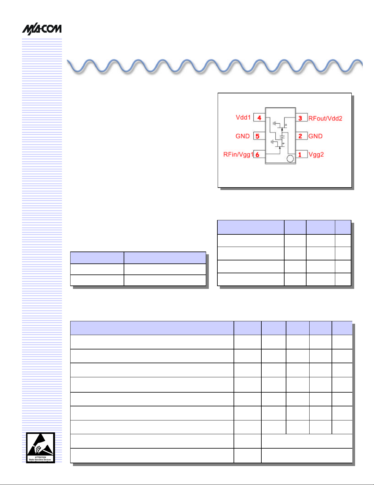
3.0 V 100 mW RF Power Amplifier
IC for Bluetooth
V 1.00
MA02305AK
Features
n 20 dB Gain – dramatically increases range of your low
power Bluetooth devices
n Single 3.0V positive supply – operates over a wide
range of supply voltages
n Extremely small size – 6 pin SOT plastic package -
3 mm x 1.75 mm body size
n Output power easily controllable via V
n 45% Power Added Efficiency
n 100% Duty Cycle
n 2000 to 2900 MHz Operation
n Self-Aligned MSAG
®
-Lite MESFET Process
DD1
Description
The MA02305AK is an RF power am plifier based on M/ACOM’s Self-Aligned MSAG MESFET Process. This
product is designed for use in 2.4 GHz ISM products as a
booster for high power Bluetooth devices. Output power
can be controlled to meet Bluetooth requirements via varying input power or the voltage on V
DD1
.
Ordering Information
Part Number Package
MA02305AK-R7 7 inch, 3000 Piece Reel
MA02305AK-SMB MA02305AK Test Board
MA02305AK
Maximum Ratings (T
Rating
DC Supply Voltage VDD 5.5 V
RF Input Power PIN 10 mW
Junction Temperature TJ 150 °C
Storage Temperature Range T
= 25 °C unless otherwise noted)
A
Symbol Value Unit
-40 to +150 °C
STG
Electrical Characteristics: V
Characteristic Symbol Min Typ Max Unit
Frequency Range ƒ 2400 2500 MHz
Output Power f = 2450 MHz P
Power Added Efficiency f = 2450 MHz η 40 45 %
Harmonics 2ƒ
Input VSWR - 1.5 2.0 :1
Off Isolation (VDD=0 V) S21 -25 dB
Thermal Resistance, junction to soldering point (pin 2) RTH 180 °C/W
Load Mismatch (VDD = 5.5 V, VSWR = 8:1, PIN = 0 dBm) - No Degradation in Power Output
Stability (P
= 0dBm, VDD = 0-5.5 V, Load VSWR = 5:1, fixed phases) - All non-harmonically related outputs
IN
= 2.5 V, V
DD1
= 3 V, P
DD2
= +0 dBm, Duty Cycle = 100%, T
IN
18.7 20 dBm
OUT
3ƒ
-30
-27
more than 60 dB below desired signal
A
-26
-22
= 25°C
dBc
Page 2
3.0 V 100 mW RF Power Amplifier IC for Bluetooth
Output Power (dBm)
Pout (dBm), PAE
Pout (dBm), PAE
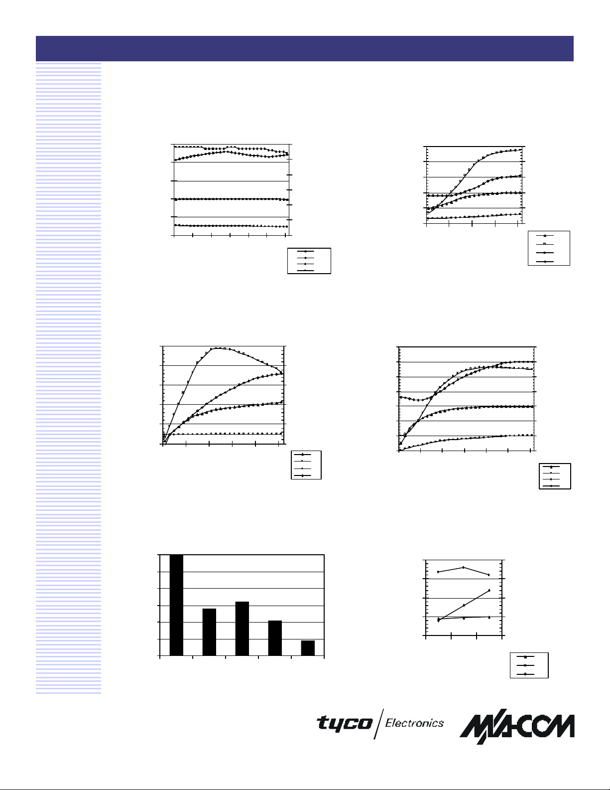
Typical Performance Curves
Output Power, Drain Currents, and Efficiency vs.
Frequency V
DD2
= 3 V , V
= 2.5 V, P
DD1
= 0 dBm
IN
MA02305AK
V 1.00
Output Power, Drain Currents and Efficiency vs.
Input Power V
= 3 V , ƒ = 2450 MHz, V
DD2
DD1
= 2.5V
50
40
30
65
55
45
35
20
10
Pout (dBm), PAE (%)
0
2300 2350 2400 2450 2500 2550 2600
Frequency (MHz)
25
15
5
Pout
PAE
Id1
Id2
Output Power, Drain Currents and Efficiency vs.
Supply Voltage
P
= 0 dBm , ƒ = 2450 MHz, V
IN
50
40
30
20
10
DD1
= 2.5 V
100
80
60
40
20
Pout (dBm), PAE (%)
0
0 1 2 3 4 5
VD2 (volts)
0
Pout
PAE
Id1
Id2
Id1, Id2 (mA)
Output Power, Drain Currents and Efficiency vs.
V
P
IN
Id1, Id2 (mA)
50
40
30
(%)
20
10
0
-15 -10 -5 0 5
Input Power (dBm)
for Power Control
DD1
= 0 dBm , ƒ = 2450 MHz, V
60
50
40
30
20
10
0
Pout (dBm), PAE (%)
-10
0.0 0.5 1.0 1.5 2.0 2.5 3.0
VD1 (volts)
DD2
= 3 V
100
80
60
40
20
0
70
60
50
40
30
20
10
0
Id1, Id2 (mA)
Pout
PAE
Id1
Id2
Id1, Id2 (mA)
Pout
PAE
Id1
Id2
Specifications subject to change without notice.
n North America: Tel. (800) 366-2266
n Asia/Pacific: Tel.+81-44-844 -8296, Fax +81-44-844-8298
n Europe: Tel. +44 (1344) 869 595, Fax+44 (1344) 300 020
Visit www.macom.com for additional data sheets and product information.
Harmonics
P
= 0 dBm , ƒ0 = 2450 MHz, V
IN
20
10
0
-10
-20
-30
-40
fo 2fo 3fo 4fo 5fo
= 2.5V, V
DD1
DD2
= 3V
Output Power, Input Return Loss and Efficiency
vs. Temperature
P
= 0 dBm , ƒ = 2450 MHz, V
IN
50
40
30
(%)
20
10
-40 25 80
Temperature (C)
= 2.5 V, V
DD1
= 3 V
DD2
-10
-15
-20
-25
-30
Input Return Loss (dB)
Pout
PAE
IRL
Page 3

3.0 V 100 mW RF Power Amplifier IC for Bluetooth
Mechanical Data
C1
MA02305AK
V 1.00
C4
C2
C5
R1
L1
Component layout and printed circuit drawing for evaluation board.
Application Information
List of Components for MA02305AK:
Part Value Manufacturer Size Part Number
C1 100 pF Dielectric Labs 0805 C11AH101K8TXL
C2 100 pF Murata 0603 GRM39C0G101J050AD
C3 100 pF Murata 0603 GRM39C0G101J050AD
C4 4700 pF Murata 0603 GRM39X7R471K
C5 1.5 pF Dielectric Labs 0603 C06CF1R5B5UL
C6 0.5 pF Dielectric Labs 0805 C11AH0R5B8TXL
R1 210 Ohm Panasonic 0603 ERJ-3EKF2100
L1 2.7 nH Toko 0603 LL1608-F2N7S
L2 22 nH Coilcraft 0603 0603HC-22NXJBU
RFin
C2
L1
Vdd1
0.120.26
C6
C1
0.27*
4
5
6
L2
C3
Vdd2
C4
0.18
L2
0.15*
3
0.05*
2
1
C3
C6
RFout
C5
E valuation Board Schematic. 50 Ω transmission line lengths in inches based on 10 mil thick, FR4. Critical line lengths denoted with (*).
Specifications subject to change without notice.
n North America: Tel. (800) 366-2266
n Asia/Pacific: Tel.+81-44-844 -8296, Fax +81-44-844-8298
n Europe: Tel. +44 (1344) 869 595, Fax+44 (1344) 300 020
Visit www.macom.com for additional data sheets and product information.
Vgg1 Vgg2
R1
0.28*
3
Page 4

3.0 V 100 mW RF Power Amplifier IC for Bluetooth
Designing With the MA02305AK
The MA02305AK is built using a near -enhancement mode FET that operates from a single supply voltage. A negative voltage is not required because the FET is designed to operate with a +0V DC gate bias.
There is no impedance matching or RF choking on this IC – these functions are supplied externally. This approach
offers the highest level of performance.
To duplicate MA02305AK data sheet performance, your circuit board must recreate the same impedances developed
on the evaluation board depicted in the preceding figures. One-port S-parameters looking into the board impedances
away from the device are listed below. The calibration plane for the datasheet is the pin of the device.
MA02305AK
V 1.00
Frequency
(MHz)
GHz MAG ANG MAG ANG MAG ANG MAG ANG
V
Pin 1 RF
GG2
OUT/VDD2
0.10 0.97043 179.42 0.71433 139.99 0.95319 152.14 0.17741 -126.15
0.20 0.99055 174.22 0.60534 129.51 0.98326 162.08 0.15709 -145.68
0.30 0.99177 171.32 0.47048 120.60 0.98368 173.64 0.16001 -151.45
0.40 0.98788 168.52 0.33247 111.57 0.97982 -174.63 0.16851 -154.29
0.50 0.98749 165.67 0.26397 107.46 0.98418 178.14 0.18235 -156.15
0.60 0.98721 162.81 0.19530 103.28 0.98820 170.74 0.19827 -158.65
0.70 0.98736 159.91 0.14041 110.03 0.98958 166.96 0.21441 -161.89
0.80 0.98679 157.04 0.08519 120.66 0.99031 163.16 0.23162 -165.23
0.90 0.98706 154.23 0.07177 135.30 0.98996 160.07 0.24969 -168.85
1.00 0.98788 151.34 0.06349 153.01 0.98991 156.76 0.26778 -173.43
1.10 0.98726 148.45 0.06587 169.91 0.98978 153.72 0.28514 -178.11
1.20 0.98626 145.60 0.07191 -174.26 0.98931 150.61 0.30267 176.84
1.30 0.98641 142.71 0.08315 -166.96 0.98780 147.19 0.31953 171.23
1.40 0.98644 139.82 0.09505 -160.56 0.98649 143.63 0.33628 165.32
1.50 0.98500 136.88 0.10675 -157.86 0.94242 143.98 0.35222 159.06
1.60 0.98453 133.95 0.11951 -155.52 0.89784 144.34 0.36683 152.71
1.70 0.98446 130.94 0.12963 -155.34 0.94174 139.92 0.38061 145.84
1.80 0.98349 127.91 0.14015 -154.79 0.98750 135.30 0.39320 138.74
1.90 0.98313 124.92 0.14882 -155.14 0.98984 132.06 0.40495 131.52
2.00 0.98382 121.96 0.15720 -155.31 0.99198 128.73 0.41623 124.12
2.10 0.98452 118.98 0.16432 -155.56 0.99283 125.72 0.42563 116.58
2.20 0.98438 115.96 0.17177 -156.08 0.99454 122.46 0.43485 108.81
2.30 0.98388 112.89 0.17810 -156.67 0.99489 119.34 0.44313 101.04
2.40 0.98292 109.77 0.18392 -157.01 0.99429 116.09 0.45009 93.13
2.50 0.98095 106.65 0.18976 -157.26 0.99242 112.85 0.45667 85.39
2.60 0.98047 103.48 0.19541 -157.75 0.99221 109.40 0.46135 77.68
2.70 0.97883 100.30 0.20085 -157.91 0.98695 105.78 0.46780 70.00
2.80 0.97676 97.12 0.20642 -157.88 0.98054 102.09 0.47186 62.56
2.90 0.97636 94.00 0.21257 -158.32 0.94404 98.07 0.47850 55.39
3.00 0.97572 90.90 0.21802 -158.71 0.90652 93.92 0.48427 48.41
Specifications subject to change without notice.
n North America: Tel. (800) 366-2266
n Asia/Pacific: Tel.+81-44-844 -8296, Fax +81-44-844-8298
n Europe: Tel. +44 (1344) 869 595, Fax+44 (1344) 300 020
Visit www.macom.com for additional data sheets and product information.
Pin 3 V
Pin 4 RFIN/V
DD1
GG1
Pin 6
4
Page 5

3.0 V 100 mW RF Power Amplifier IC for Bluetooth
Frequency
(MHz)
GHz MAG ANG MAG ANG MAG ANG MAG ANG
3.10 0.97519 87.69 0.22473 -158.80 0.92813 94.32 0.49202 41.58
3.20 0.97443 84.47 0.23177 -158.99 0.95106 94.75 0.49805 35.13
3.30 0.97243 81.27 0.24068 -159.25 0.96150 90.58 0.50499 28.91
3.40 0.97032 78.11 0.24969 -159.62 0.97174 86.31 0.51221 22.98
3.50 0.96903 74.98 0.26052 -160.44 0.96351 82.36 0.51994 17.31
3.60 0.96701 71.74 0.27111 -161.00 0.95413 78.37 0.52764 11.82
3.70 0.96360 68.63 0.28211 -161.90 0.93047 76.80 0.53520 6.57
3.80 0.96292 65.58 0.29396 -162.97 0.91064 75.14 0.54388 1.67
3.90 0.96262 62.38 0.30492 -164.32 0.93350 71.90 0.55281 -3.06
4.00 0.96034 59.13 0.31552 -165.45 0.95344 68.60 0.56144 -7.62
4.10 0.95820 55.98 0.33008 -167.00 0.95477 64.91 0.57003 -11.96
4.20 0.95728 52.79 0.34582 -168.67 0.95909 61.22 0.57934 -15.94
4.30 0.95652 49.53 0.36052 -170.75 0.95625 57.65 0.58809 -19.92
4.40 0.95406 46.40 0.37552 -172.64 0.95056 54.21 0.59686 -23.71
4.50 0.95198 43.31 0.39089 -175.10 0.94539 50.71 0.60531 -27.27
4.60 0.95125 40.19 0.40622 -177.54 0.94197 47.20 0.61438 -30.62
4.70 0.95152 37.10 0.42189 179.59 0.93401 43.41 0.62434 -33.90
4.80 0.95166 33.99 0.44003 176.61 0.92723 39.69 0.63385 -37.21
4.90 0.95067 30.77 0.45429 173.31 0.90236 35.79 0.64268 -40.26
5.00 0.94774 27.57 0.46894 169.93 0.87776 32.01 0.65242 -43.36
5.10 0.94351 24.50 0.48131 166.56 0.84543 31.67 0.65976 -46.33
5.20 0.94210 21.54 0.49478 163.09 0.81564 31.34 0.66830 -49.11
5.30 0.94232 18.59 0.50530 159.43 0.85067 29.15 0.67776 -51.79
5.40 0.94193 15.72 0.51842 155.69 0.88431 27.07 0.68668 -54.49
5.50 0.94382 12.78 0.52984 151.82 0.89525 23.25 0.69550 -57.16
5.60 0.94635 9.68 0.54223 147.54 0.90655 19.42 0.70606 -59.79
5.70 0.94601 6.52 0.54973 143.21 0.90262 15.33 0.71713 -62.63
5.80 0.94421 3.50 0.55888 138.79 0.89847 11.62 0.72678 -65.49
5.90 0.94367 0.68 0.56482 134.44 0.88135 8.25 0.73521 -68.25
6.00 0.94249 -2.19 0.56973 130.04 0.86517 5.04 0.74383 -71.11
V
Pin 1 RF
GG2
OUT/VDD2
Pin 3 V
Pin 4 RFIN/V
DD1
MA02305AK
V 1.00
Pin 6
GG1
Specifications subject to change without notice.
n North America: Tel. (800) 366-2266
n Asia/Pacific: Tel.+81-44-844 -8296, Fax +81-44-844-8298
n Europe: Tel. +44 (1344) 869 595, Fax+44 (1344) 300 020
Visit www.macom.com for additional data sheets and product information.
 Loading...