

Page 1
RF Power Amplifier IC
for 2.4 GHz ISM
MA02303GJ
Features
• Perfect for 802.11B, HOP, SWAP, HOMERF,
Bluetooth, WDECT, MDS, MMDS
• Single Positive Supply
• Power Added Efficiency As High As 55 Percent
• IP
= +43 dBm
3
• Output Power 26.5 dBm @ 3.3 V
• Output Power 28.5 dBm @ 5.0 V
• 100 Percent Duty Cycle
• 2200 to 2600 MHz Operation
• 8 Pin MSOP Full Downset Plastic Package
• Operates Over Wide Ranges of Supply Voltage
• Self-Aligned MSAG
®
-Lite MESFET Process
Description
The MA02303GJ is an RF power amplifier based on
M/A-COM’s Self-Aligned MSAG MESFET Process.
This product is designed for use in 2.4 GHz ISM
products. For booster applications, it features a low
power “bypass” mode and output power control
Ordering Information
Part Number Description
MA02303GJ-R7 7 inch, 1000 piece reel
MA02303GJ-R13 13 inch, 3000 piece reel
MA02303GJ-SMB Sample test board
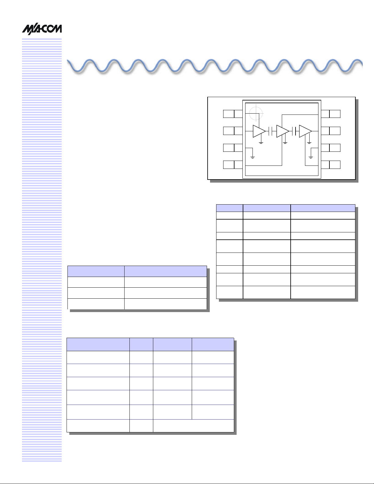
Functional Schematic
PIN 1
PIN Configuration
PIN Function Description
1
2
3 GND Ground
4
5
6 GND Ground
7
8
Package bottom is electrical and thermal ground
V
RF
V
V
RF
V
D1
G2
G3
D2
IN
OUT
/ V
/ V
G1
D3
Drain voltage, first stage
RF input and drain
voltage for first stage
Gate bias voltage,
second stage
Gate bias voltage,
third stage
RF output and drain
voltage for third stage
Drain voltage for
second stage
PIN 8
Absolute Maximum Ratings 1
Rating Symbol Value Unit
DC Supply Voltage
RF Input Power
Junction Temperature
Storage Temperature
Operating Temperature
Moisture Sensitivity
1. Beyond these limits, the device may be damaged or device reliability
reduced. Functional operation at absolute-maximum-rated conditions is
not implied.
VDD
P
IN
T
J
T
STG
T
OPER
JEDEC Level 1
5.5 V
10 mW
150 °C
-40 to +150 °C
-40 to +100 °C
Page 2
RF Power Amplifier IC for 2.4 GHz ISM
MA02303GJ
Electrical Specifications: V
= +3.3 V, P
DD
= -2 dBm, Duty Cycle = 100 %,
IN
TS = 37 °C (Note 1), measured on evaluation board shown in Figure 11.
Characteristic Symbol Min. Typ. Max. Unit
Frequency Range
Output Power, ƒ = 2450 MHz
Power Added Efficiency, ƒ = 2450 MHz η
Current, ƒ = 2450 MHz
Current for linear operation, ƒ = 2450 MHz,
PIN adjusted for P
= 20.0 dBm +/- 0.2 dBm
OUT
Gain, ƒ = 2450 MHz,
PIN adjusted for P
= 20.0 dBm +/- 0.2 dBm
OUT
Harmonics, ƒ = 2450 MHz
Input VSWR, ƒ = 2450 MHz
Off Isolation (V
DD
=0 V)
Thermal Resistance, junction to package bottom
Third Order Intercept Point
Load Mismatch (V
Stability (P
IN
= 5.5 V, VSWR = 8:1, PIN = 0 dBm)
DD
= -2 to 2 dBm, VDD = 0-5.5 V, Load VSWR = 5:1,
all phases)
ƒ 2400 2500 MHz
P
OUT
I
DD
I
DD
G 29.5 dB
2ƒ, 3ƒ, 4 ƒ -40 dBc
— — 2.0:1 —
— 40 dB
R
TH
IP
3
—
—
25.3 26.5 — dBm
51 %
265 415 mA
415 mA
25
43 dBm
No Degradation in Power Output
All non-harmonically related outputs more
than 60 dB below desired signal
°C/W
1. TS is the temperature measured at the soldering point of the downset paddle on the bottom of the IC.
Specifications subject to change without notice.
n North America: Tel. (800) 366-2266
n Asia/Pacific: Tel.+81-44-844-8296, Fax +81-44-844-8298
n Europe: Tel. +44 (1344) 869 595, Fax+44 (1344) 300 020
Visit www.macom.com for additional data sheets and product information.
2
Page 3
RF Power Amplifier IC for 2.4 GHz ISM
B
DD
B
DD
B
B
DD
B
DD
DD1
DD2
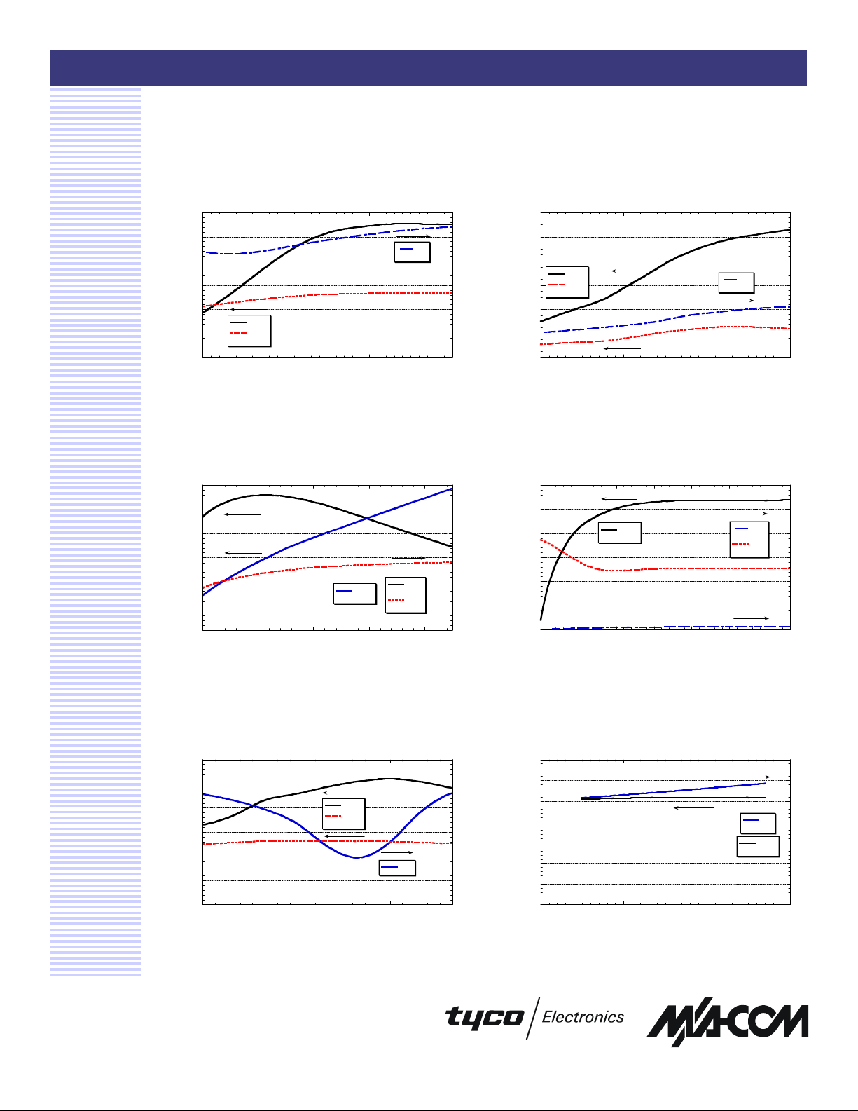
Typical Characteristics
(Measured data from process nominal devices)
MA02303GJ
Output Power, Drain Current and
Efficiency vs. Input Power
60
50
40
30
20
(dBm), PAE (%)
OUT
10
P
0
-10 -5 0 5
PAE
P
OUT
V
= 3.3 V
DD1, 2, 3
F = 2450 MHz
PIN (dBm)
Output Power, Drain Current and Efficiency
vs. Supply Voltage
60
50
40
30
20
(dBm), PAE (%)
OUT
10
P
0
PAE
P
OUT
PIN = -2 dBm
F = 2450 MHz
P
OUT
I
DD
1 2 3 4 5
PIN (dBm)
PAE
I
DD
Output Power, and Drain Current vs. Input
Power for Low Current “Bypass” Mode
(V
= 3.3 V, V
DD1,2
300
250
I
DD
200
150
100
50
0
(mA)
I
(dBm), PAE (%)
OUT
P
12
10
8
PAE
6
P
OUT
4
2
0
-10 -5 0 5
= 0.0 V)
DD3
V
= 3.3 V, V
DD1, 2
F = 2450 MHz
DD3
= 0.0 V
300
250
200
I
DD
150
100
(mA)
I
50
0
PIN (dBm)
Output Power, Drain Current and Efficiency
for Power Control
DD1
P
OUT
600
500
I
I
DD1
DD2
400
300
200
(mA)
, I
I
100
0
V
(V)
DD1
0.35
0.30
0.25
0.20
0.15
0.10
0.05
(A)
I
vs. V
30
25
20
15
(dBm)
OUT
10
P
5
0
0.0 0.5 1.0 1.5 2.0 2.5 3.0
Output Power, Input Return Loss and
Efficiency vs. Frequency
60
50
40
30
20
(dBm), PAE (%)
OUT
P
P
= - 2 dBm
IN
VDD = 3.3 V
10
0
2200 2300 2400 2500 2600
FREQUENCY (MHz)
Specifications subject to change without notice.
PAE
P
OUT
IRL
0
-5
-10
-15
-20
-25
-30
IRL (dB)
Output Power and Drain Current vs.
Temperature at VDD = +3.0 V
35
30
25
20
(dBm)
15
OUT
P
PIN = - 2 dBm
10
VDD - 3.0 V
5
F = 2450 MHz
0
-50 0 50 100
Temperature, TS (oC)
350
300
250
I
200
DD
P
OUT
150
(mA)
I
100
50
0
3
n North America: Tel. (800) 366-2266
n Asia/Pacific: Tel.+81-44-844-8296, Fax +81-44-844-8298
n Europe: Tel. +44 (1344) 869 595, Fax+44 (1344) 300 020
Visit www.macom.com for additional data sheets and product information.
Page 4

RF Power Amplifier IC for 2.4 GHz ISM
B
DD
B
DD
Typical Characteristics (Cont’d)
(Measured data from process nominal devices)
MA02303GJ
Output Power and Drain Current vs.
Temperature at V
35
30
25
20
(dBm)
15
OUT
P
10
PIN = - 2 dBm
VDD - 3.2 V
5
F = 2450 MHz
0
-50 0 50 100
= +3.2 V
DD
Temperature, TS (oC)
Harmonics
(dBm)
OUT
P
-10
-15
-20
30
25
20
15
10
5
0
-5
ƒ0 2ƒ0 3ƒ0 4ƒ0
PIN = -2dBm
= 2450MHz
ƒ
0
VDD = 3.3V
Output Power and Drain Current vs.
Temperature at V
(mA)
I
35
30
25
20
(dBm)
15
OUT
P
PIN = - 2 dBm
10
VDD - 3.6 V
5
F = 2450 MHz
0
-50 0 50 100
350
300
250
200
I
DD
150
P
OUT
100
50
0
= +3.6V
DD
Temperature, TS (oC)
350
300
250
200
I
DD
P
OUT
150
(mA)
I
100
50
0
Maximum Operating Temperature (Ts) to
Maintain <150 °C Junction Temperature.
6
5
OUT
- P
4
DD3
3
* V
DD
2
(W) = I
1
DISS
P
0
-50 0 50 100 150
Temperature TS (oC)
Specifications subject to change without notice.
4
n North America: Tel. (800) 366-2266
n Asia/Pacific: Tel.+81-44-844-8296, Fax +81-44-844-8298
n Europe: Tel. +44 (1344) 869 595, Fax+44 (1344) 300 020
Visit www.macom.com for additional data sheets and product information.
Page 5

RF Power Amplifier IC for 2.4 GHz ISM
DD
L2 1 2 3 4 5 6 7 8 T2
T1
R1
T5
Downset Paddle
T7
Mechanical Data
Figure 11 Component layout and printed circuit drawing for evaluation board (60 mil GETEK
board).
Application Information
MA02303GJ
+V
C2
C3
RFIN
T3
C1
Figure 12 Evaluation Board Schematic
L1
T4
List of Components
Discrete Components Transmission Line Lengths*
C1 – C4 = 100 pF multilayer ceramic chip capacitor
(Dielectric Labs C11AH101K5TXL)
C5 = 2.0 pF multilayer ceramic chip capacitor
(Dielectric Labs C11AH2R0BTXL)
C6 = 1.2 pF multilayer ceramic chip capacitor
(Dielectric Labs C11AH1R2B5TXL)
R1 = 300 Ω chip resistor (P300ECT-ND)
L1 = 1.8 nH chip inductor (Toko TKS235CT-ND)
L2 = 27 nH chip inductor (Coilcraft 1008CS-270XKBB)
*The board material is 0.060" FR-4 (distance is between RF and GND) with a dielectric constant of
about 4.3 (standard FR-4)
Specifications subject to change without notice.
n North America: Tel. (800) 366-2266
n Asia/Pacific: Tel.+81-44-844-8296, Fax +81-44-844-8298
n Europe: Tel. +44 (1344) 869 595, Fax+44 (1344) 300 020
Visit www.macom.com for additional data sheets and product information.
Full-
To Board Ground
C4
T8
RF
OUT
T6
C5
C6
T1 = 0.15"
T2 = 0.21"
T3 = 0.11" (Not very critical)
T4 = 0.16"
T5 = 0.13"
T6 = 0.16"
T7 = 0.13" (Not very critical)
T8 = 0.077" (Not very critical)
T1, T2, T3, T5, T6 are 0.077" wide
T4, T7, and T8 are 0.026" wide
5
Page 6

RF Power Amplifier IC for 2.4 GHz ISM
Designing with the MA02303GJ
The MA02303GJ is built using a near-enhancement mode FET that operates from a single supply voltage. A negative
voltage is not required because the FET is designed to operate with a +0V DC gate bias.
There is no impedance matching or RF choking on this IC – these functions are supplied externally. This approach
offers the highest level of performance, the lowest bill of materials cost, and far fewer components than a discrete design.
To duplicate MA02303GJ data sheet performance, your circuit board must recreate the same impedances developed on
this evaluation board. The table below has one-port s-parameter measurements looking into the traces on the evaluation board. S-parameters of the MA02303GJ are not supplied because the device is designed to operate under largesignal conditions.
MA02303GJ
Frequency V
GHz Mag Ang Mag Ang Mag Ang Mag Ang Mag Ang
0.2 0.98890 168.89 0.98437 158.43 0.98990 157.75 0.96758 88.92 0.98740 170.03
0.3 0.88449 130.14 0.97810 148.00 0.98811 147.07 0.93440 52.01 0.87259 126.11
0.4 0.96296 162.21 0.96932 138.02 0.98733 136.83 0.89791 28.02 0.95647 168.46
0.5 0.98166 159.36 0.96033 128.52 0.98729 126.92 0.85525 8.85 0.97951 165.71
0.6 0.98669 150.11 0.95221 119.37 0.98779 117.53 0.80306 -8.42 0.98325 157.06
0.7 0.98659 142.94 0.94257 110.68 0.98796 108.67 0.75165 -23.19 0.98331 150.64
0.8 0.98701 136.46 0.93372 102.50 0.98912 100.34 0.70235 -36.51 0.98362 144.92
0.9 0.98696 130.40 0.92399 94.78 0.98928 92.48 0.65785 -49.03 0.98291 139.57
1.0 0.98757 124.64 0.91521 87.48 0.99004 85.10 0.61674 -61.22 0.98248 134.49
1.1 0.98793 119.13 0.90655 80.60 0.99099 78.16 0.58189 -73.60 0.98325 129.55
1.2 0.98766 113.79 0.89741 74.13 0.99165 71.67 0.55207 -86.36 0.98254 124.75
1.3 0.98685 108.52 0.88850 68.01 0.99162 65.55 0.52778 -99.76 0.98097 119.95
1.4 0.98253 103.08 0.87922 62.20 0.99228 59.78 0.51054 -113.87 0.97567 114.77
1.5 0.91016 98.26 0.87041 56.61 0.99283 54.27 0.50134 -128.62 0.88506 109.11
1.6 0.97895 96.95 0.85901 51.24 0.99372 49.02 0.50184 -143.72 0.96660 110.93
1.7 0.98693 91.94 0.84867 46.25 0.99362 44.08 0.51099 -159.03 0.97912 105.76
1.8 0.98885 87.51 0.83780 41.39 0.99411 39.33 0.52890 -174.06 0.98174 101.51
1.9 0.98968 83.39 0.82602 36.67 0.99457 34.73 0.55378 171.57 0.98247 97.56
2.0 0.99001 79.46 0.81268 32.09 0.99405 30.31 0.58373 158.06 0.98252 93.75
2.1 0.98939 75.68 0.79856 27.65 0.99409 26.02 0.61689 145.85 0.96646 89.86
2.2 0.99079 72.12 0.78264 23.35 0.99430 21.85 0.65283 133.76 0.98349 87.18
2.3 0.99100 68.61 0.76563 19.11 0.99427 17.75 0.68573 123.12 0.98395 83.71
2.4 0.99134 65.25 0.74652 14.96 0.99425 13.76 0.71788 113.31 0.98474 80.41
2.5 0.99146 61.98 0.72506 10.91 0.99399 9.82 0.74798 104.32 0.98447 77.23
2.6 0.99178 58.73 0.70186 6.91 0.99400 5.85 0.77528 95.95 0.98507 74.04
2.7 0.99134 55.49 0.67587 2.97 0.99331 1.90 0.79976 88.27 0.98381 70.83
2.8 0.98781 52.20 0.64683 -0.91 0.99282 -2.00 0.82079 81.13 0.98006 67.52
2.9 0.96980 48.90 0.61470 -4.81 0.99214 -5.98 0.83832 74.49 0.96403 63.91
3.0 0.95172 48.55 0.57400 -8.86 0.99108 -9.98 0.85400 68.30 0.90400 62.55
3.1 0.98242 46.16 0.52740 -11.19 0.98954 -13.99 0.86663 62.57 0.95087 63.65
3.2 0.99063 43.08 0.48956 -13.34 0.98827 -18.12 0.87801 57.07 0.97696 60.24
3.3 0.99392 40.27 0.44620 -15.29 0.98684 -22.42 0.88698 51.92 0.98397 57.19
3.4 0.99353 37.51 0.40182 -16.23 0.98579 -26.81 0.89353 46.93 0.98539 54.35
3.5 0.99183 34.87 0.35797 -15.65 0.98338 -31.29 0.89823 42.18 0.98374 51.69
3.6 0.98528 32.36 0.31683 -13.12 0.98114 -36.02 0.90042 37.52 0.97595 49.24
Pin 1 RFIN/V
DD1
Pin 2 V
GG1
Pin 4 RF
GG2
Pin 7 V
OUT/VDD3
DD2
Pin 8
Specifications subject to change without notice.
n North America: Tel. (800) 366-2266
n Asia/Pacific: Tel.+81-44-844-8296, Fax +81-44-844-8298
n Europe: Tel. +44 (1344) 869 595, Fax+44 (1344) 300 020
Visit www.macom.com for additional data sheets and product information.
6
Page 7

RF Power Amplifier IC for 2.4 GHz ISM
Designing with the MA02303GJ (Cont’d)
MA02303GJ
Frequency V
GHz Mag Ang Mag Ang Mag Ang Mag Ang Mag Ang
3.7 0.98115 30.74 0.28368 -7.89 0.97774 -40.95 0.89832 32.95 0.97468 47.68
3.8 0.99055 28.59 0.26456 -0.17 0.97527 -46.15 0.88711 28.34 0.98255 45.41
3.9 0.99468 26.15 0.26206 8.43 0.97149 -51.66 0.85217 23.98 0.98187 42.91
4.0 0.99541 23.85 0.27526 16.18 0.96801 -57.48 0.78439 25.69 0.97076 41.20
4.1 0.99675 21.53 0.30017 21.62 0.96214 -63.64 0.91321 26.53 0.98240 39.66
4.2 0.99695 19.34 0.33169 24.71 0.95817 -70.37 0.95402 19.53 0.98870 37.44
4.3 0.99709 17.08 0.36614 25.86 0.95218 -77.52 0.95927 14.12 0.99033 35.21
4.4 0.99625 14.89 0.40041 25.61 0.94464 -85.24 0.95907 9.50 0.99064 33.12
4.5 0.99600 12.71 0.43430 24.41 0.93766 -93.67 0.95776 5.12 0.99008 31.05
4.6 0.99528 10.53 0.46785 22.33 0.92733 -102.87 0.95648 0.78 0.98931 29.00
4.7 0.99356 8.29 0.49729 18.61 0.90989 -112.87 0.95538 -3.70 0.98729 26.91
4.8 0.98985 6.02 0.50830 15.70 0.89316 -122.91 0.95299 -8.40 0.98183 24.79
4.9 0.98183 3.77 0.53008 12.03 0.87835 -135.47 0.94875 -13.35 0.96994 22.79
5.0 0.96606 1.91 0.51899 5.22 0.76901 -147.15 0.94290 -18.71 0.94954 21.59
5.1 0.95907 1.19 0.48184 8.12 0.80492 -149.68 0.93754 -24.50 0.95096 21.58
5.2 0.97380 -0.08 0.51026 7.72 0.86212 -162.69 0.93242 -31.40 0.96888 20.35
5.3 0.98447 -2.18 0.52064 4.75 0.87712 -176.53 0.92307 -39.86 0.97525 18.47
5.4 0.98993 -4.47 0.51978 2.19 0.88096 170.41 0.90396 -50.55 0.98503 17.01
5.5 0.99206 -6.71 0.51313 -0.14 0.88478 157.90 0.86790 -64.94 0.99094 14.98
5.6 0.99234 -8.95 0.50465 -2.02 0.89099 145.89 0.79942 -85.01 0.99192 13.15
5.7 0.99149 -11.15 0.49217 -3.82 0.89655 134.39 0.69417 -115.75 0.99221 11.35
5.8 0.98990 -13.42 0.47394 -5.03 0.90165 123.67 0.55561 -163.96 0.99216 9.58
5.9 0.98628 -15.52 0.45693 -5.12 0.90854 113.69 0.51158 134.06 0.99070 7.95
6.0 0.98532 -17.49 0.44346 -4.72 0.91522 104.42 0.59033 85.74 0.98983 6.41
Pin 1 RFIN/V
DD1
Pin 2 V
GG1
Pin 4 RF
GG2
Pin 7 V
OUT/VDD3
DD2
Pin 8
MSOP-8EP (Downset Lead)
PIN 8
E1
E
15°
L
PIN 1
A2
e
D
A
A1
b
Specifications subject to change without notice.
n North America: Tel. (800) 366-2266
n Asia/Pacific: Tel.+81-44-844-8296, Fax +81-44-844-8298
n Europe: Tel. +44 (1344) 869 595, Fax+44 (1344) 300 020
Visit www.macom.com for additional data sheets and product information.
MAX
Theta θ
D1
E2
EXPOSED PAD
MSOP-8
Dim Measurement (mm)
Min. Max. Min. Max.
A 0.80 1.10 0.0315 0.0433
A1 0.26 0.076 0.0010 0.0030
A2 0.75 0.95 0.0295 0.0374
b 0.25 0.40 0.0098 0.0157
D 2.90 3.10 0.1142 0.1220
D1 1.85 ref. 1.85 ref. 0.073 ref. 0.073 ref.
E 4.90
basic
4.90
basic
E1 2.90 3.10 0.1142 0.1220
E2 1.73 ref. 1.73 ref. 0.068 ref. 0.068 ref.
e 0.65
basic
0.65
basic
L 0.40 0.70 0.0157 0.0276
Theta (θ)
Note: All dimensions per JEDEC MO-187 Var. AA (issue B)
except for D1, E2, and A1. See JEDEC or contact M/A-COM
for additional dimensional and tolerance information.
0o 6
Measurement (inches)
0.1929
basic
0.0256
basic
o
0o 6o
0.1929
basic
0.0256
basic
7
 Loading...