

Page 1
MA02206GJ
3.6V 0.5W RF Power Amplifier IC
for DECT
FEATURES
•= Single Positive Supply
•= 57% Power Added Efficiency
•= Operation down to 1.2 V
•= 100% Duty Cycle
•= 1800 to 2000 MHz Operation
•= 8 Pin Full Downset MSOP Plastic Package
•= Accommodates Battery Charging Conditions up to
5.6 Volts
•= Self-Aligned MSAG
®
-Lite MESFET Process
8 Lead MSOP Package
Package bottom is electrical and thermal ground
DESCRIPTION MAXIMUM RATINGS (Beyond these limits, the device may be damaged or device
reliability reduced. Functi onal operation at absolute–maximum–rated conditions is not implied.)
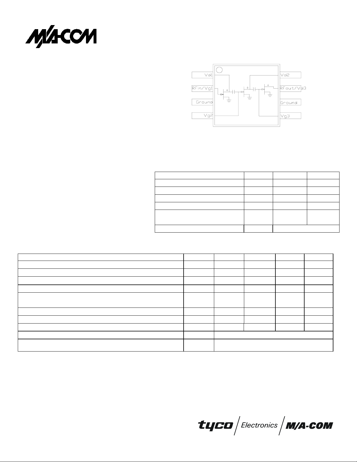
The MA02206GJ is a DECT Power amplifier
based on M/A-COM’s Self-Aligned MSAG
MESFET Process. This product is designed
for use in 3.6 V DECT handsets and base
stations.
Rating Symbol Value Unit
DC Supply Voltage VDD 6.0 V
RF Input Power PIN 10 mW
Junction Temperature TJ 150 °C
Storage Temperature Range T
Operating Temperature
T
STG
OPER
-40 to +150
-40 to +100
Range
Moisture Sensitivity
JEDEC Level 1
ELECTRICAL CHARACTERISTICS V
board shown in Figure 9.
Characteristic Symbol Min Typ Max Unit
= +3.6 V, PIN= -2 dBm, Duty Cycle = 100 %, TS = 37 °C (Note 1), measured on evaluation
DD
Frequency Range ƒ 1880 1900 1930 MHz
Output Power (1900 MHz)
Power Added Efficiency (1900 MHz)
Drain Current (1900MHz)
Harmonics
P
25.9 26.9 27.9 dBm
OUT
η
52 57 %
IDD 228 330 mA
2ƒo
3ƒ
-37
o
-38
-30
-34
Input VSW R — 1.3:1 2.0:1 —
Off Isolat ion (V
Thermal Resistance, Junct i on to soldering point (T
Load Mismatch (V
Stability (P
Note 1: T
Note 2: Output power and efficiency have been optimized for input drive levels between –2 to +2 dBm. Stability is only specified within this range. For
is the temperature m easured at the soldering point of the downset paddl e on the bottom of the IC.
s
operation outside of this range, contact the fact ory.
=0 V) — 38 44 dB
DD
= 4.5 V, VSW R = 5: 1, P
DD
= -2 to 2 dBm, V
IN
) (Note 1) —
s
= -2 dBm) —
IN
= 0-5.0 V, Load VSWR = 5:1, all phases) —
DD
No Degradation in Power Output
All non-harmonically related outputs more than
25
60 dB below desired signal
°C
°C
dBc
°C/W
Specifications subject to change without notice.
North America: Tel. (800)366-2266, Fax (800)618-8883
Asia/Pacific: Tel. +81-44-844-8296, Fax +81-44-844-8298
Europe: Tel. +44 (1344) 869 595, Fax +44 (1344) 300 020
Visit www.macom.com for additional data sheets and product information
902407 E
Page 2
3.6V 0.5W RF Power Amplifier IC for DECT MA02206GJ
TYPICAL CHARACTERISTICS (Measured data from process nomi nal devi ces)
6
5
OUT
- P
4
DD3
* V
3
DD3
2
(W) = I
DISS
P
1
0
-50 0 50 100 150
Temperature, T
(°C)
S
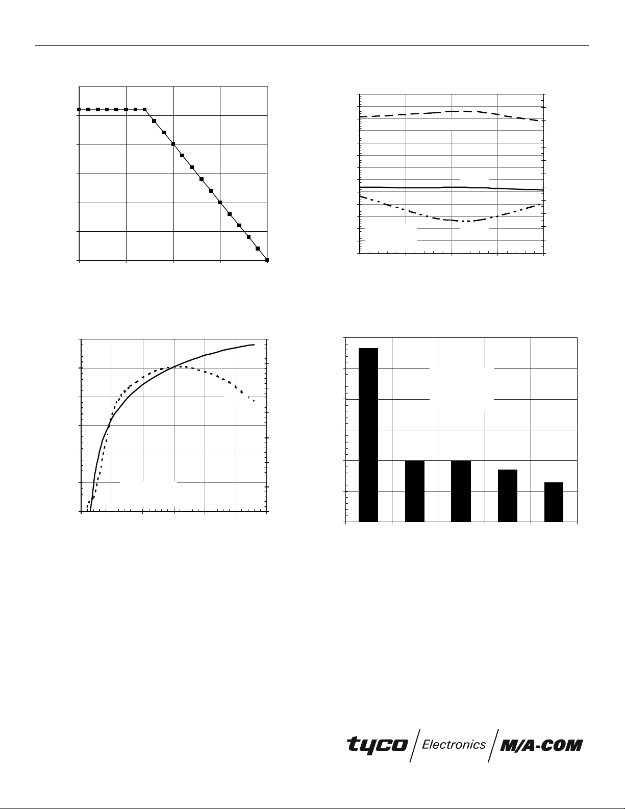
Figure 1. Maximum operating temperature (TS) to
maintain <150°C junction temperature.
65
60
55
50
45
40
35
30
25
20
15
Pout (dBm) and PAE (%)
10
VDD = 3.6 V
5
P
= -2 dBm
IN
0
1800 1850 1900 1950 2000
PAE
P
OUT
VSWR
Frequency (MHz)
6.0
5.5
5.0
4.5
4.0
3.5
3.0
2.5
2.0
1.5
1.0
0.5
0.0
VSWR
Figure 2. Output power, power added efficiency, and
input VSWR vs. frequency
30
25
P
OUT
70
60
50
20
PAE
40
15
(dBm)
OUT
P
30
PAE (%)
10
20
5
PIN = -2 dBm
10
f = 1900 MHz
0
0
0123456
Supply Voltage (Volts)
Figure 3. Output power and power added efficiency vs.
supply voltage
30
20
10
-10
-20
-30
VDD = 3.6 V
P
= -2 dBm
IN
f
= 1900 MHz
o
0
ƒο 2ƒο 3ƒο 4ƒο 5ƒο
Figure 4. Harmonics
Specifications subject to change without notice.
North America: Tel. (800)366-2266, Fax (800)618-8883
Asia/Pacific: Tel. +81-44-844-8296, Fax +81-44-844-8298
Europe: Tel. +44 (1344) 869 595, Fax +44 (1344) 300 020
Visit www.macom.com for additional data sheets and product information
902407 E
Page 3

3.6V 0.5W RF Power Amplifier IC for DECT MA02206GJ
T
T
T
TYPICAL CHARACTERISTICS (Measured data f rom process nominal devi ces)
30
25
300
P
OU
250
30
25
P
OU
300
250
I
20
15
(dBm )
OUT
P
DD
10
PIN = -2 dBm
5
V
DD
= 3. 0 V
Freq=1900 MHz
0
-50 0 50 100
Tem pera ture T
(°C)
S
Figure 5. Output power and drain current vs.
temperature at V
30
25
20
15
(dBm)
OUT
P
10
5
0
-50 0 50 100
P
OU
I
DD
Temperature T
=+3.0V
DD
PIN = -2 dBm
V
= 3.6 V
DD
Freq=1900 MHz
(°C)
S
Figure 7. Output power and drain current vs.
temperature at V
=+3.6V
DD
200
150
100
50
0
300
250
200
150
100
50
0
(ma )
I
(ma)
I
DD
DD
I
20
15
(dBm)
OUT
P
10
DD
200
150
100
(ma)
I
DD
PIN = -2 dBm
5
V
DD
= 3.2 V
50
Freq=1900 MHz
0
0
-50050100
Temperature T
(°C)
S
Figure 6. Output power and drain current vs.
temperature at VDD=+3.2V
Specifications subject to change without notice.
North America: Tel. (800)366-2266, Fax (800)618-8883
Asia/Pacific: Tel. +81-44-844-8296, Fax +81-44-844-8298
Europe: Tel. +44 (1344) 869 595, Fax +44 (1344) 300 020
Visit www.macom.com for additional data sheets and product information
902407 E
Page 4

3.6V 0.5W RF Power Amplifier IC for DECT MA02206GJ
APPLICATION INFORMATION
+V
RF
DD
C2 C4
T7
IN
T1
C1
T2
L1
R1
T3
T4
L2
1
2
3
4
C3
Full-Downset Paddle
To Board Ground
T8
L3
8
7
6
5
T5
C5
RF
C6
Figure 8. Evaluation Board Schematic
List of components: Transmission Lines (Grounded Coplanar Waveguide)
C1 = 0.7 pF multilayer ceramic chip capacitor T1 = 0.140” 50 Ω
C2 = C3 = C4 = C6 = 100 pF multilayer ceramic chip capacitor T2 = 0.110” 50 Ω
C5 = 2.2 pF multilayer ceramic chip capacitor T3 = 0.100” 50 Ω
L1 = 2.7 nH chip inductor T4 = 0.400” 75 Ω
L2 = 3.3 nH chip inductor T5 = 0.195” 50 Ω
L3 = 27 nH chip inductor T6 = 0.280” 50 Ω
R1 = 300 Ω chip resistor T7=78 = 0.090” 75 Ω=
60 mil GETEK Board
OUT
Figure 9. Evaluation Board Layout
Specifications subject to change without notice.
North America: Tel. (800)366-2266, Fax (800)618-8883
Asia/Pacific: Tel. +81-44-844-8296, Fax +81-44-844-8298
Europe: Tel. +44 (1344) 869 595, Fax +44 (1344) 300 020
Visit www.macom.com for additional data sheets and product information
Figure 10. 50 ΩΩΩΩ Lead Transition
902407 E
Page 5

3.6V 0.5W RF Power Amplifier IC for DECT MA02206GJ
DESIGNING WITH THE MA02206GJ
The MA02206GJ is built using a near-enhanc ement mode FET that operates from a single supply voltage. A negative
voltage is not required because the FET is designed to operate with a +0V DC gate bias.
There is no impedance matching or RF choking on this IC – these functions ar e supplied exter nally. T his
approach offers the highest level of performance, the lowest bill of materials cost, and far fewer components
than a discrete design.
Output power and efficiency have been optimized for DECT conditions. Input power must be kept between –2 and
+2dBm.
To duplicate MA02206GJ data s heet performance, your circuit boar d must recreate the sam e impedances developed on
this evaluation board. The table below has one-port s-param eter m easurements looking into the traces on the evaluation
board. S-param eters of the MA02206GJ are not supplied because the device is designed to oper ate under large-signal
conditions.
Freq V
GHz Mag Ang Mag Ang Mag Ang Mag Ang Mag Ang
0.2 0.98045 178.38 0.15583 92.45 0.98634 159.96 0.53341 119.98 0.99255 178.98
0.3 0.94299 158.86 0.34874 -79.64 0.99012 150.97 0.32398 106.05 0.97095 163.41
0.4 0.97932 -171.16 0.61727 89.09 0.98896 141.89 0.20397 98.78 0.98118 -178.46
0.5 0.98910 -178.37 0.53105 68.98 0.98414 132.81 0.10550 90.87 0.98448 -176.22
0.6 0.99498 177.21 0.81116 49.51 0.98671 124.13 0.01912 95.87 0.99955 176.46
0.7 0.99236 174.45 0.87096 32.24 0.98308 115.73 0.05548 -108.06 0.99916 173.24
0.8 0.99399 172.25 0.84304 20.09 0.98482 107.57 0.12170 -111.09 1.00072 170.74
0.9 0.99541 170.17 0.86887 16.78 0.98514 99.90 0.18593 -116.17 1.00140 168.47
1.0 0.99503 168.20 0.87209 9.18 0.98562 92.35 0.24519 -121.18 1.00119 166.28
1.1 0.99279 166.32 0.87044 1.42 0.97997 85.32 0.30304 -126.47 0.99926 164.20
1.2 0.99285 164.31 0.83274 -4.47 0.98220 78.49 0.35920 -131.80 0.99991 161.99
1.3 0.99423 162.46 0.80852 -11.26 0.98249 72.12 0.41315 -137.20 0.99956 159.92
1.4 0.98574 159.89 0.74573 -16.03 0.98284 65.97 0.46330 -142.60 0.99277 157.02
1.5 0.88116 157.23 0.66751 -21.70 0.97828 60.11 0.51088 -148.03 0.86762 154.31
1.6 0.97552 161.35 0.60211 -24.92 0.98255 54.23 0.55789 -153.43 0.98555 158.39
1.7 0.98767 158.42 0.53753 -28.44 0.98167 48.79 0.59900 -158.95 0.99642 155.25
1.8 0.99039 156.35 0.45804 -27.44 0.98173 43.48 0.63867 -164.21 0.99918 152.78
1.9 0.99244 154.61 0.41128 -25.54 0.98234 38.27 0.67512 -169.36 1.00119 150.69
2.0 0.98742 152.93 0.36682 -20.92 0.97956 33.43 0.70454 -174.44 0.99355 148.30
2.1 0.99010 151.31 0.34855 -16.52 0.97866 28.52 0.73360 -178.67 0.88062 147.26
2.2 0.98911 149.68 0.32313 -13.38 0.97966 23.87 0.76239 175.86 0.99684 146.97
2.3 0.99139 148.11 0.30695 -8.01 0.98028 19.13 0.78572 171.11 1.00029 144.53
2.4 0.98809 146.33 0.30024 -0.16 0.97910 14.65 0.80560 166.68 1.00005 142.46
2.5 0.99058 144.56 0.32491 3.85 0.97652 10.29 0.82474 162.24 1.00010 140.35
2.6 0.98513 142.80 0.32429 4.54 0.97751 5.87 0.83818 157.93 0.99560 138.31
2.7 0.98991 140.66 0.31415 7.56 0.97715 1.53 0.86018 153.55 0.99891 136.04
2.8 0.97904 138.58 0.31418 14.28 0.97600 -2.68 0.87076 149.33 0.98388 133.36
2.9 0.94926 136.15 0.33349 18.76 0.97526 -7.00 0.88376 145.18 0.95012 130.27
3.0 0.90603 138.55 0.36476 23.39 0.97179 -11.28 0.89423 141.16 0.86390 133.79
3.1 0.96258 137.61 0.43170 21.35 0.96761 -15.40 0.90136 136.54 0.95789 133.92
3.2 0.97824 135.30 0.42416 18.54 0.96919 -19.53 0.90933 132.45 0.97992 130.74
Pin 1 RFIN/V
DD1
Pin 2 V
GG1
Pin 4 RF
GG2
OUT/VDD3
Pin 7 V
DD2
Pin 8
Specifications subject to change without notice.
North America: Tel. (800)366-2266, Fax (800)618-8883
Asia/Pacific: Tel. +81-44-844-8296, Fax +81-44-844-8298
Europe: Tel. +44 (1344) 869 595, Fax +44 (1344) 300 020
Visit www.macom.com for additional data sheets and product information
902407 E
Page 6

3.6V 0.5W RF Power Amplifier IC for DECT MA02206GJ
Freq V
GHz Mag Ang Mag Ang Mag Ang Mag Ang Mag Ang
3.3 0.98600 133.22 0.44491 18.34 0.96815 -23.97 0.92075 128.19 0.99110 128.32
3.4 0.97581 131.03 0.46286 15.87 0.96856 -28.22 0.91634 123.51 0.98056 125.59
3.5 0.97510 128.55 0.47492 13.72 0.96669 -32.53 0.92419 117.78 0.98100 122.36
3.6 0.95375 126.87 0.48711 11.01 0.96540 -36.99 0.91573 111.37 0.95666 119.66
3.7 0.95057 127.45 0.49197 7.38 0.96407 -41.44 0.88717 101.63 0.93969 117.38
3.8 0.97376 125.97 0.48573 2.45 0.96212 -46.11 0.67487 79.43 0.80350 109.35
3.9 0.97682 123.62 0.46779 -0.28 0.96054 -50.67 0.46027 156.66 0.86651 131.73
4.0 0.98005 121.79 0.45180 -4.24 0.96034 -55.50 0.84398 132.42 0.96565 124.03
4.1 0.98137 119.83 0.42656 -7.50 0.95559 -60.49 0.91747 120.75 0.98040 119.87
4.2 0.97884 118.09 0.39991 -11.55 0.95544 -65.64 0.94120 113.77 0.98556 117.40
4.3 0.97918 116.42 0.36462 -15.55 0.95345 -70.99 0.95303 108.35 0.98601 114.89
4.4 0.97904 114.45 0.32379 -19.79 0.95303 -76.48 0.96185 103.78 0.98684 112.78
4.5 0.97991 112.45 0.27421 -24.08 0.95103 -82.34 0.96948 99.46 0.98870 110.59
4.6 0.97809 110.26 0.21778 -28.21 0.94710 -88.30 0.97059 95.22 0.98453 108.46
4.7 0.96567 108.32 0.15094 -30.95 0.94266 -94.72 0.96901 91.36 0.97623 106.45
4.8 0.96153 105.69 0.07907 -24.06 0.93632 -101.21 0.97053 87.30 0.97255 104.06
4.9 0.93877 103.67 0.03254 37.56 0.93172 -108.15 0.96542 83.54 0.94871 102.09
5.0 0.89436 102.91 0.11563 93.79 0.90196 -115.16 0.95436 79.82 0.90915 101.96
5.1 0.88960 104.77 0.17035 81.80 0.91026 -120.16 0.94874 76.13 0.92284 103.31
5.2 0.92614 104.42 0.20983 84.90 0.92716 -128.19 0.93975 72.37 0.95245 102.11
5.3 0.94661 102.27 0.26841 84.54 0.92694 -136.71 0.93430 68.62 0.96874 99.91
5.4 0.95985 100.14 0.32306 81.90 0.92817 -145.26 0.92552 64.45 0.97597 98.06
5.5 0.96135 97.63 0.36853 77.62 0.92438 -154.07 0.91055 60.10 0.97767 95.99
5.6 0.95723 95.59 0.40466 73.11 0.91805 -163.10 0.89467 55.88 0.97522 94.27
5.7 0.95195 93.78 0.43174 69.62 0.91529 -172.11 0.88144 51.26 0.97159 92.53
5.8 0.94291 92.04 0.45333 66.86 0.90561 178.78 0.86118 45.92 0.96476 91.00
5.9 0.94307 90.43 0.48474 63.83 0.91067 169.22 0.84235 39.69 0.96887 89.52
6.0 0.94249 89.05 0.50533 59.87 0.90904 159.64 0.81197 32.21 0.96766 87.98
Pin 1 RFIN/V
DD1
Pin 2 V
GG1
Pin 4 RF
GG2
OUT/VDD3
Pin 7 V
DD2
Pin 8
Specifications subject to change without notice.
North America: Tel. (800)366-2266, Fax (800)618-8883
Asia/Pacific: Tel. +81-44-844-8296, Fax +81-44-844-8298
Europe: Tel. +44 (1344) 869 595, Fax +44 (1344) 300 020
Visit www.macom.com for additional data sheets and product information
902407 E
 Loading...