

Page 1
1/32May 2003
M93S66, M93S56
M93S46
4Kbit, 2Kbit and 1Kbit (16-bit wide)
MICROWIRE Serial Access EEPROM with Block Protection
FEATURES SUMMARY
■ Industry Standard MICROWIRE Bus
■ Single Supply Voltage:
– 4.5V to 5.5V for M93Sx6
– 2.5V to 5.5V for M93Sx6-W
– 1.8V to 5.5V for M93Sx6-R
■ Single Organization: by Word (x16)
■ Programming Instructions that work on: Word or
Entire Memory
■ Self-timed Programming Cycle with Auto-Erase
■ User Defined Write Protected Area
■ Page Write Mode (4 words)
■ Ready/Busy Signal During Programming
■ Speed:
– 1MHz Clock Rate, 10ms Write Time (Current
product, identified by process identification
letter F or M)
– 2MHz Clock Rate, 5ms Write Time (New
Product, identified by process identification
letter W)
■ Sequential Read Operation
■ Enhanced ESD/Latch-Up Behavior
■ More than 1 Million Erase/Write Cycles
■ More than 40 Year Data Retention
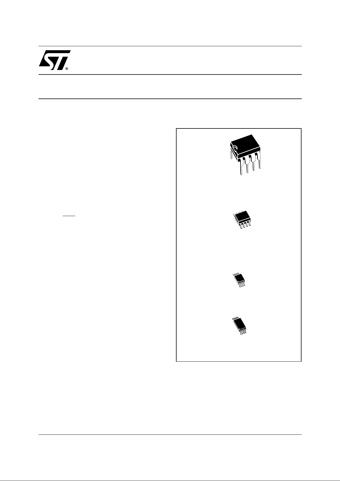
Figure 1. Packages
PDIP8 (BN)
8
1
SO8 (MN)
150 mil width
8
1
TSSOP8 (DW)
169 mil width
TSSOP8 (DS)
3x3mm body size
Page 2
M93S66, M93S56, M93S46
2/32
SUMMARY DESCRIPTION
This specification covers a range of 4K, 2K, 1K bit
serial Electrically Erasable Programmable Memory (EEPROM) products (respectively for M93S66,
M93S56, M93S46). In this text, these products are
collectively referred to as M93Sx6.
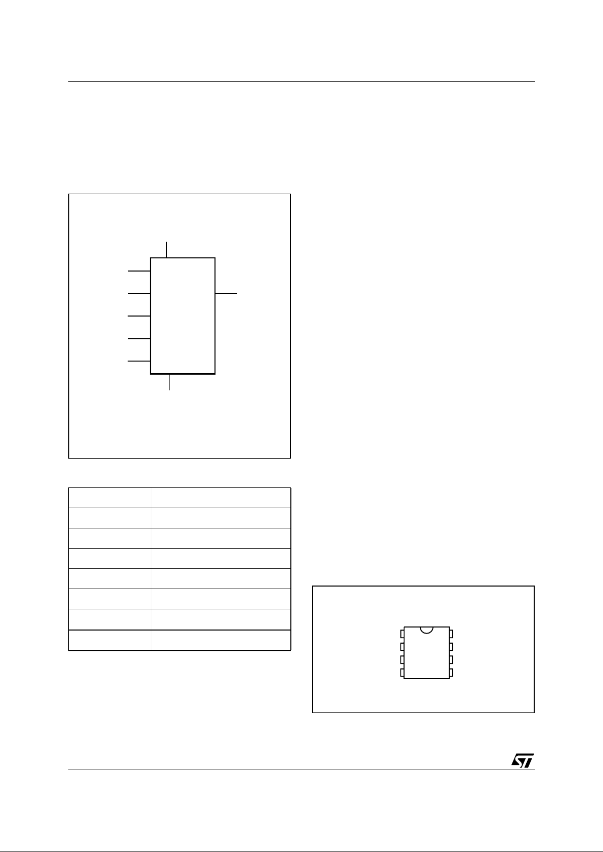
Figure 2. Logic Diagram
Table 1. Signal Names
The M93Sx6 is accessed through a serial input (D)
and output (Q) us in g the MICROWIRE bus protocol. The memory is divided into 256, 128, 64 x16
bit words (respectively for M93S66, M93S56,
M93S46).
The M93Sx6 is accessed by a set of instructions
which includes Read, W rite, Page Write, Write All
and instructions used to set the memory protection. These are summarized in Table 2 and 3).
A Read Data from Memory (READ) instruction
loads the address of the first word to be read into
an internal address pointer. The data contained at
this address is then clocked out serially. The address pointer is automatically incremented after
the data is output and, if the Chi p S elect Input (S)
is held High, the M93Sx6 can output a sequ ential
stream of data words. In this way, the memory can
be read as a data stream from 16 to 4096 bits (for
the M93S66), or continuously as the address
counter automatically rolls over to 0 0h when the
highest address is reached.
Within the time required by a programming cycle
(t
W
), up to 4 words may be written with help of the
Page Write instruction. the whole memory may
also be erased, or set to a predetermined pattern,
by using the Write All instruction.
Within the memory, a us er defined area may be
protected against further Write instructions. The
size of this area is defined by the content of a Protection Register, located outside of the memory
array. As a final protection step, data may be permanently protected by programm ing a One Time
Programming bit (OT P bit) which l ocks t he Prote ction Register content.
Programming is internal ly self-timed (the external
clock signal on Serial Clock (C) may be stopped or
left running after the start of a Write cycle) and
does not require an erase cycle prior to the Write
instruction. The Write instruction writes 16 bits at a
time into one of the word locations of the M93Sx6,
the Page Write instruction writes up to 4 words of
16 bits to sequential locations, assum ing in both
cases that all addresses are outside the Write Protected area. After the start of the programming cycle, a Busy/Ready signal is available on Serial
Data Output (Q) when Chip Select Input (S) is
driven High.
Figure 3. DIP, SO and TSSOP Connections
Note: 1. See page 26 (onwards) for package dimensions, and how
to identify pin-1.
S Chip Select Input
D Serial Data Input
Q Serial Data Output
C Ser ial Clock
PRE Protection Register Enable
W Write Enable
V
CC
Supply Voltage
V
SS
Ground
AI02020
D
V
CC
M93Sx6
V
SS
C Q
PRE
W
S
V
SS
Q
W
PREC
SV
CC
D
AI02021
M93Sx6
1
2
3
4
8
7
6
5
Page 3

3/32
M93S66, M93S56, M93S46
An internal Power-on Data P rot ection m ec hani sm
in the M93Sx6 inhibits the device when the supply
is too low.
POWER-ON DATA PROTECTION
To prevent data corruption and inadvertent write
operations during power-up, a Power-On Reset
(POR) circuit resets all internal programming circuitry, and sets the device in the Write Disable
mode.
– At Power-up and P ower-down, the device must
not be selected (that is, Chip Select Input (S)
must be driven Low) until the supply voltage
reaches the operating value V
CC
specified in
Table 5 to Table 6.
– When V
CC
reaches its valid level, the d evice is
properly reset (in the Write Disabl e mode) and
is ready to decode and execute incoming instructions.
For the M93Sx6 devices (5V range) the POR
threshold voltage is around 3 V. For the M 93Sx6W (3V range) and M93Sx6-R (2V range) the POR
threshold voltage is around 1.5V.
INSTRUCTIONS
The instruction set of the M93Sx6 devices contains seven instructions, as summarized in Table 2
to Table 3. Each instruction consists of the following parts, as shown in Figure 4:
■ Each instruction is preceded by a rising edge on
Chip Select Input (S) with Serial Clock (C) being
held Low.
■ A start bit, which is the first ‘1’ read on Serial
Data Input (D) during the rising edge of Serial
Clock (C).
■ Two op-code bits, read on Serial Data Input (D)
during the rising edge of Serial Clock (C).
(Some instructions also use the first two bits of
the address to define the op-code).
■ The address bits of the byte or word that is to be
accessed. For the M93S46, the address is
made up of 6 bits (see Table 2). For the M93S56
and M93S66, the address is made up of 8 bits
(see Table 3).
The M93Sx6 devices are fabricated in CMOS
technology and are therefore able to run as slow
as 0 Hz (static input signals) or as fast as t he maximum ratings specified in Table 16 to Table 19.
Page 4
M93S66, M93S56, M93S46
4/32
Table 2. Instruction Set for the M93S46
Note: 1. X = Don’t Care bit.
Instruction Description W PRE
Start
bit
Op-
Code
Address
1
Data
Required
Clock
Cycles
Additional
Comments
READ
Read Data
from Memory
X 0 1 10 A5-A0 Q15-Q0
WRITE
Write Data to
Memory
1 0 1 01 A5-A0 D15-D0 25
Write is executed if
the address is not
inside the Protected
area
PAWRITE
Page Write to
Memory
1 0 1 11 A5-A0
N x
D15-D0
9 + N x 16
Write is executed if
all the N addresses
are not inside the
Protected area
WRAL
Write All
Memory
with same
Data
1 0 1 00 01 XXXX D15-D0 25
Write all data if the
Protection Register
is cleared
WEN Write Enable 1 0 1 00 11 XXXX 9
WDS Write Disable X 0 1 00 00 XXXX 9
PRREAD
Protection
Register Read
X 1 1 10 XXXXXX
Q5-Q0
+ Flag
Data Output =
Protection Register
content + Protection
Flag bit
PRWRITE
Protection
Register Write
1 1 1 01 A5-A0 9
Data above specified
address A5-A0 are
protected
PRCLEAR
Protection
Register Clear
1 1 1 11 111111 9
Protect Flag is also
cleared (cleared
Flag = 1)
PREN
Protection
Register
Enable
1 1 1 00 11XXXX 9
PRDS
Protection
Register
Disable
1 1 1 00 000000 9
OTP bit is set
permanently
Page 5
5/32
M93S66, M93S56, M93S46
Table 3. Instruction Set for the M93S66, M93S56
Note: 1. X = Don’t Care bit.
2. Address bit A7 is not decoded by the M93S 56.
Instruction Description W PRE
Start
bit
Op-
Code
Address
1,2
Data
Required
Clock
Cycles
Additional
Comments
READ
Read Data
from Memory
X 0 1 10 A7-A0 Q15-Q0
WRITE
Write Data to
Memory
1 0 1 01 A7-A0 D15-D0 27
Write is executed if
the address is not
inside the
Protected area
PAWRITE
Page Write to
Memory
1 0 1 11 A7-A0
N x
D15-D0
11 + N x 16
Write is executed if
all the N
addresses are not
inside the
Protected area
WRAL
Write All
Memory
with same
Data
1 0 1 00 01XXXXXX D15-D0 27
Write all data if the
Protection
Register is cleared
WEN Write Enable 1 0 1 00 11XXXXXX 11
WDS Write Disable X 0 1 00 00XXXXXX 11
PRREAD
Protection
Register Read
X 1 1 10 XXXXXXXX
Q7-Q0
+ Flag
Data Output =
Protection
Register content +
Protection Flag bit
PRWRITE
Protection
Register Write
1 1 1 01 A7-A0 11
Data above
specified address
A7-A0 are
protected
PRCLEAR
Protection
Register Clear
1 1 1 11 11111111 11
Protect Flag is also
cleared (cleared
Flag = 1)
PREN
Protection
Register
Enable
1 1 1 00 11XXXXXX 11
PRDS
Protection
Register
Disable
1 1 1 00 00000000 11
OTP bit is set
permane ntly
Page 6
M93S66, M93S56, M93S46
6/32
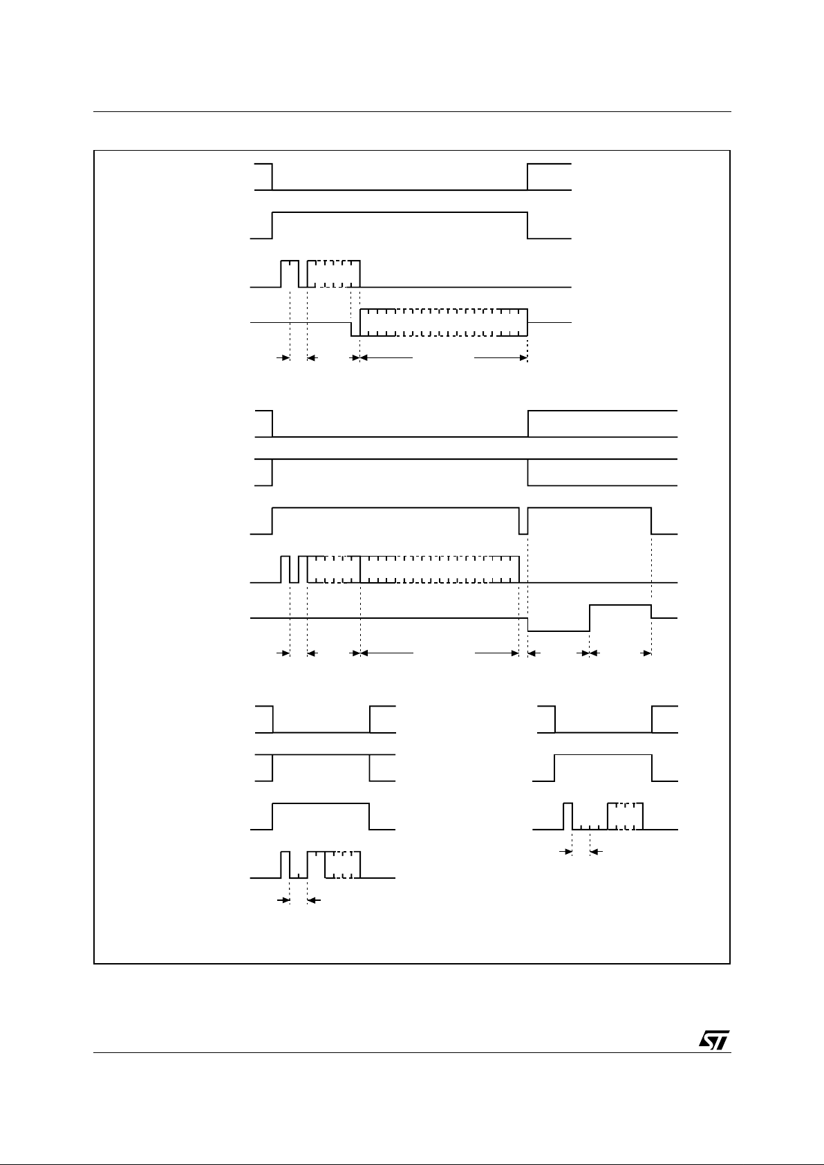
Figure 4. READ, WRITE, WEN and WDS Sequences
Note: For the mea ni ngs of An, Xn, Qn and Dn, see Ta bl e 2 and Table 3.
AI00889D
1 1 0 An A0
Qn Q0
DATA OUT
D
S
Q
S
WRITE
ADDR
OP
CODE
1 0An A0
DATA IN
D
Q
OP
CODE
Dn D01
BUSY READY
S
WRITE
ENABLE
1 0XnX0D
OP
CODE
101
S
WRITE
DISABLE
1 0XnX0D
OP
CODE
0 00
CHECK
STATUS
ADDR
PREREAD
PRE
W
PRE
W
PRE
Page 7

7/32
M93S66, M93S56, M93S46
Read
The Read Data from Memory (READ) instruction
outputs serial data on Serial Data Output (Q).
When the instruction is received, the op-code and
address are decoded, and the data from the memory is transferred to an output shift register. A dummy 0 bit is output first, followed by the 16-bit word,
with the most significant bit first. Output data
changes are triggered by the rising edge of Serial
Clock (C). The M93Sx6 au tomatically increments
the internal address register and clocks out the
next byte (or word) as long as the Chip Select Input (S) is held High. In this case, the dummy 0 bit
is not output between bytes (or words) and a continuous stream of data can be read.
Write Enable and Write Disable
The Write Enable (WEN) instruction enables the
future execution of write instructions, and the Write
Disable (WDS) instruction disables it. When power
is first app lied, the M9 3Sx6 initializes itse l f s o that
write instructions are disabled. After an Write Enable (WEN) instruction has been executed, writing
remains enabled until an Write Disable (WDS) instruction is exe cuted, or until V
CC
falls below the
power-on reset threshold voltage . To protect the
memory contents from accidental corruption, it is
advisable to issue the Write Disable (WDS) instruction after every write cycle. The Read Data
from Memory (READ) instruction is not affected by
the Write Enable (WEN) or Write Disable (WDS)
instructions.
Write
The Write Data to Memory (WRITE) instruction is
composed of the Start bit plus the op-code followed by the address and the 16 data bits to be
written.
Write Enable (W) mus t be held High before and
during the instruction. Input a ddress and data, on
Serial Data Input (D) are sampled on the rising
edge of Serial Clock (C).
After the last data bit has been sampled, the C hip
Select Input (S) must be taken Low before the next
rising edge of Serial Clock (C). If Chip Select Input
(S) is brought Low before or after this specific time
frame, the self-timed programming cycle will not
be started, and the addressed location will not be
programmed.
While the M93Sx6 is performing a write cycle, but
after a delay (t
SLSH
) before the s tatus inform ation
becomes available, Chip S elect Input (S) can be
driven High to monitor the status of the write cycle:
Serial Data Output (Q) is driven Low while the
M93Sx6 is still busy, and High when the cycle is
complete, and the M93Sx6 is ready to receive a
new instruction. The M93Sx6 ignores any data on
the bus while it is busy on a wri te cycle. O nce t he
M93Sx6 is Ready, Serial Data Output (Q) is driven
High, and remains in this state until a new start bit
is decoded or the Chip Select Input (S) is brought
Low.
Programming is internally self-timed, so the external Serial Clock (C) may be disconnected o r left
running after the start of a write cycle.
Page 8
M93S66, M93S56, M93S46
8/32
Figure 5. PA WR I TE and WRAL Sequence
Note: For the mea ni ngs of An, Xn an d Dn, please see Table 2 and Table 3.
Page Write
A Page Write to Memory (PAWRITE) instruction
contains the first address to be written, followed by
up to 4 data words.
After the receipt of each data w ord, bits A1-A 0 of
the internal address register are incremented, the
high order bits remaining unchanged (A7-A2 for
M93S66, M93S56; A5-A2 for M93S46). Users
must take care, in the software, to ensure that the
last word address has the same upper order address bits as the initial address transmitted to
avoid address roll-over.
The Page Write to Memory (PAWRITE) instruction
will not be executed if any of the 4 words addresses the protected area.
Write Enable (W) mus t be held High before and
during the instruction. Input a ddress and data, on
Serial Data Input (D) are sampled on the rising
edge of Serial Clock (C).
After the last data bit has been sampled, the C hip
Select Input (S) must be taken Low before the next
rising edge of Serial Clock (C). If Chip Select Input
(S) is brought Low before or after this specific time
frame, the self-timed programming cycle will not
AI00890C
S
PAGE
WRITE
1 1An A0
DATA IN
D
Q
OP
CODE
Dn D01
BUSY READY
CHECK
STATUS
ADDR
PRE
W
S
WRITE
ALL
1 0XnX0
DATA IN
D
Q
OP
CODE
Dn D00
BUSY READY
CHECK
STATUS
ADDR
PRE
W
01
Page 9

9/32
M93S66, M93S56, M93S46
be started, and the addressed location will not be
programmed.
While the M93Sx6 is performing a write cycle, but
after a delay (t
SLSH
) before the s tatus inform ation
becomes available, Chip S elect Input (S) can be
driven High to monitor the status of the write cycle:
Serial Data Output (Q) is driven Low while the
M93Sx6 is still busy, and High when the cycle is
complete, and the M93Sx6 i s ready to receive a
new instruction. The M93Sx6 ignores any data on
the bus while it is busy on a wri te cycle. O nce t he
M93Sx6 is Ready, Serial Data Output (Q) is driven
High, and remains in this state until a new start bit
is decoded or the Chip Select Input (S) is brought
Low.
Programming is internally self-timed, so the external Serial Clock (C) may be disconnected o r left
running after the start of a write cycle.
Write All
The Write All Memory with same Data (WRAL) instruction is valid only after the Protection Register
has been cleared by executing a Protection Register Clear (PRCLEAR) instruction. The Write All
Memory with same Data (WRAL) instruction simultaneously writes the whole memory with the
same data word given in the instruction.
Write Enable (W) mus t be held High before and
during the instruction. Input a ddress and data, on
Serial Data Input (D) are sampled on the rising
edge of Serial Clock (C).
After the last data bit has been sampled, the C hip
Select Input (S) must be taken Low before the next
rising edge of Serial Clock (C). If Chip Select Input
(S) is brought Low before or after this specific time
frame, the self-timed programming cycle will not
be started, and the addressed location will not be
programmed.
While the M93Sx6 is performing a write cycle, but
after a delay (t
SLSH
) before the s tatus inform ation
becomes available, Chip S elect Input (S) can be
driven High to monitor the status of the write cycle:
Serial Data Output (Q) is driven Low while the
M93Sx6 is still busy, and High when the cycle is
complete, and the M93Sx6 is ready to receive a
new instruction. The M93Sx6 ignores any data on
the bus while it is busy on a wri te cycle. O nce t he
M93Sx6 is Ready, Serial Data Output (Q) is driven
High, and remains in this state until a new start bit
is decoded or the Chip Select Input (S) is brought
Low.
Programming is internally self-timed, so the external Serial Clock (C) may be disconnected o r left
running after the start of a write cycle.
Page 10
M93S66, M93S56, M93S46
10/32
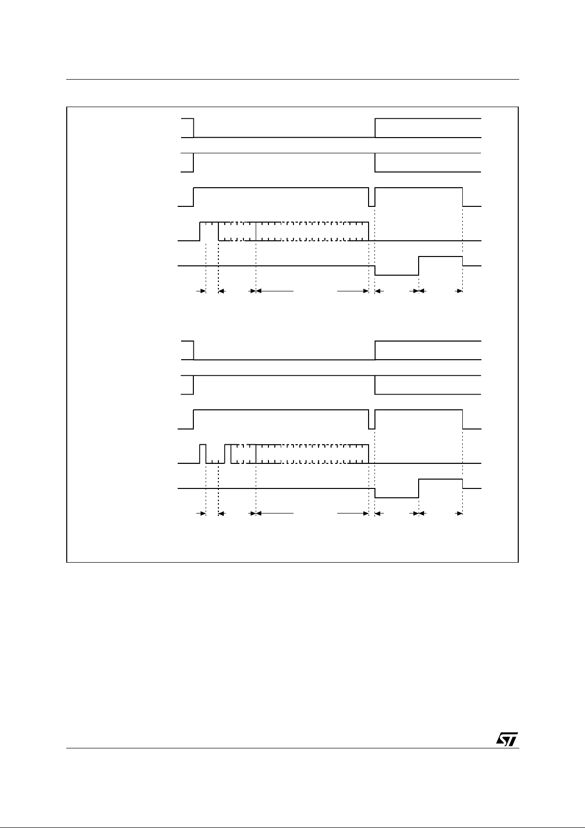
Figure 6. PREAD, PRWRITE and PREN Sequences
Note: For the mea ni ngs of An, Xn an d Dn, please see Table 2 and Table 3.
AI00891D
1 1 0 Xn X0
DATA
OUT
D
S
Q
S
Protect
Register
WRITE
ADDR
OP
CODE
1 0An A0D
Q
OP
CODE
1
BUSY READY
S
Protect
Register
ENABLE
1 0XnX0D
OP
CODE
101
CHECK
STATUS
ADDR
PREProtect
Register
READ
PRE
W
PRE
W
An A0 F
F = Protect Flag
Page 11

11/32
M93S66, M93S56, M93S46
Figure 7. PRCLEAR and PRDS Sequences
Note: For the mea ni ngs of An, Xn an d Dn, please see Table 2 and Table 3.
AI00892C
S
Protect
Register
CLEAR
1 1D
Q
OP
CODE
1
BUSY READY
CHECK
STATUS
ADDR
PRE
W
111
S
Protect
Register
DISABLE
1 0D
Q
OP
CODE
0
BUSY READY
CHECK
STATUS
ADDR
PRE
W
000
Page 12

M93S66, M93S56, M93S46
12/32
WRITE PROTECTION AND THE PROTECTION REGISTER
The Protection Register on the M93Sx6 is used to
adjust the amount of me mory that is to be write
protected. The write protected are a extends from
the address given in the Protection Register, up to
the top address in the M93Sx6 device.
Two flag bi ts are used to indicate the Protection
Register status:
– Protection Flag: this is used to enable/disable
protection of the write-protected area of the
M93Sx6 memory
– OTP bit: when set, this disables access to t he
Protection Register, and thus prev ents any further modifications to the value in the Protec tion
Register.
The lower-bound memory address is written to the
Protection Register using the Protection Register
Write (PRWRITE) instruction. It can be read using
the Protection Register Read (PRREAD) instruction.
The Protection Register Enable (PREN) instruction must be executed before any PRCLEAR,
PRWRITE or PRDS instruction, and with appropriate levels applied to the Protection Enable (PRE)
and Write Enable (W) signals.
Write-access to the Protection Register is
achieved by executing the following sequence:
– Execute the Write Enable (WEN) instruction
– Execute the Protection Register Enable (PREN)
instruction
– Execute one PRWRITE, PRCLEAR or PRDS
instructions, to set a new boundary address in
the Protection Register, to clear the protection
address (to all 1s), or permanently to freeze the
value held in the Protection Register.
Protection Register Read
The Protection Re gister Rea d (PRRE AD) instruction outputs, on Serial Data Output (Q), the content of the Protection Register, followed by the
Protection Flag bit. The Protection Enabl e (PRE)
signal must be driven High before and during the
instruction.
As with the Read Data from Memory (READ) instruction, a dummy 0 bit is output first. Since it is
not possible to distinguish between the Protec tion
Register being cleared (all 1s) or having been written with all 1s, the user must check the Protection
Flag status (and no t the Protection Regist er content) to ascertain the setting of the memory protection.
Protection Register Enable
The Protection Register Enable (PREN) instruction is used to authorize the use of instructions that
modify the Protection Register (PRWRITE,
PRCLEAR, PRDS). The P rotection Register En-
able (PREN) instruction does not modify the Protection Flag bit value.
Note: A Write Enable (WEN) instruction must be
executed before the Protection Register Enable
(PREN) instruction. Both the Protection Enable
(PRE) and Write Enable (W) signals must be driven High during the instruction execution.
Protection Register Clear
The Protection Register Clear (PRCLEAR) instruction clears the address stored in the Protection Register to all 1s, so that none of the memory
is write-protected by the Protection Register. However, it should be noted that all the memory remains protected, in the normal way, using the
Write Enable (WEN) and Write Disable (WDS) instructions.
The Protection Register Clear (PRCLEAR) instruction clears t he Protection F lag to 1. Both t he
Protection Enable (PRE) and Write Enable (W)
signals must be driven High during t he i nstruction
execution.
Note: A Protection Register Enable (PREN) instruction must immediately precede the Protection
Register Clear (PRCLEAR) instruction.
Protectio n Register Write
The Protection Register Write (PRWRITE) instruction is used to write an address into the Protection
Register. This is the address of the f ir st word t o be
protected. After the Protection Register Write
(PRWRITE) instruction has been executed, all
memory locations equal to and above the specified address are protected from writing.
The Protection Flag bit is set to 0, and can be read
with Protection Register Read (PRREAD) instruction. Both the Protection Enable (PRE) and Write
Enable (W) signals must be driven High during the
instruction execution.
Note: A Protection Register Enable (PREN) instruction must immediately precede the Protection
Register Write (PRWRITE) instruction, but it is not
necessary to execute first a Protection Register
Clear (PRCLEAR).
Protection Register Disable
The Protection Register Disable (PRDS) instruction sets the One Tim e Programmable (OTP ) bit.
This instructio n is a ONE TIME O NLY i nstruct ion
which latches the Protection Register content, this
content is therefore unalterable in the future. Both
the Protection Enable (PRE) and Write Enable (W)
signals must be driven High during t he i nstruction
execution. The OTP bit can not be di rectly read, it
can be checked by reading the content of the Protection Register, using the Protection Register
Read (PRREAD) instruction, then by writing this
same value back into the Protection Regist er, us-
Page 13

13/32
M93S66, M93S56, M93S46
ing the Protection Register Write (PRWRITE) instruction. When the OTP bit is set, the Ready/Busy
status cannot appear on Serial Da ta Output (Q).
When the OTP bit is not set, the Busy status appears on Serial Data Output (Q).
Note: A Protection Register Enable (PREN) instruction must immediately precede the Protection
Register Disable (PRDS) instruction.
COMMON I/O OPERATION
Serial Data Output (Q) and Serial Data Input (D)
can be connected toget her, through a c urrent limiting resistor, to form a common, single-wire data
bus. Some precautions must be taken when operating the memory in this way, mostly to prevent a
short circuit current from flowing when the last address bit (A0) clashes with the first data bit on Serial Data Output (Q). Please see the application
note AN394 for details.
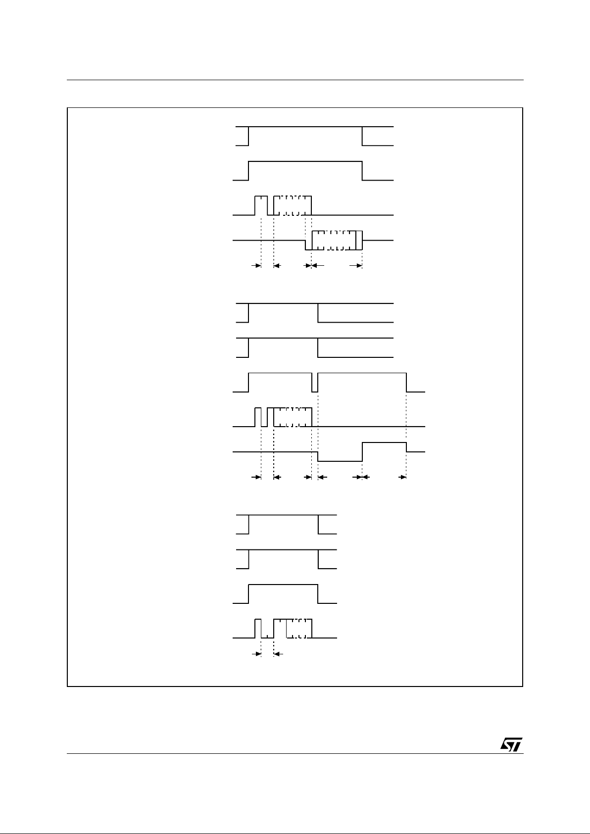
Figure 8. Write Sequence with One Clock Glitch
CLOCK PULSE COUNTER
In a noisy environment , the number of p ulses received on Serial Clock (C) may be greater than the
number delivered by the Bus Master (the microcontroller). This can lead to a misalignment of the
instruction of one or more bits (as shown in Figure
8) and may lead to the writing of erroneous data at
an erroneous address.
To combat this problem, the M 93Sx6 has an onchip counter that counts the clock pulses from the
start bit until the falling edge of the Chip Select Input (S). If the number of clock pulses received is
not the number expected, the WRI TE, P AWR ITE,
WRALL, PRWRITE or PRCLEAR instruction is
aborted, and the contents of the memory are not
modified.
The number of clock cycles expected for eac h instruction, and for each member of the M93Sx6
family, are summa rized i n T able 2 to Table 3. For
example, a Write Data to Memory (WRITE) instruction on the M93S56 (or M93S66) expects 27
clock cycles from the start bit to the falling edge of
Chip Select Input (S). That is:
1 Start bit
+ 2 Op-code bits
+ 8 Address bits
+ 16 Data bits
AI01395
S
An-1
C
D
WRITE
START
D0"1""0"
An
Glitch
An-2
ADDRESS AND DATA
ARE SHIFTED BY ONE BIT
Page 14

M93S66, M93S56, M93S46
14/32
MAXI MUM RATI N G
Stressing the device ab ove the rating listed in t he
Absolute Maximum Ratings" table may cause permanent damage to the device. These are stress
ratings only and operation of the device at t hese or
any other conditions ab ove those i ndicated in t he
Operating sections of this specificat ion is not im-
plied. Exposure to Absolute Maximum Rating conditions for extended periods may affect device
reliability. Refer also to the STMicroelectronics
SURE Program and other relevan t quality documents.
Table 4. Absolute Maximum Ratings
Note: 1. IPC/JEDEC J-STD-02 0A
2. JED EC St d JESD22-A 114A (C1=100 pF, R1=1500 Ω, R2=500 Ω)
Symbol Parameter Min. Max. Unit
T
STG
Storage Temperature –65 150 °C
T
LEAD
Lead Temperature during
Soldering
PDIP: 10 seconds
SO: 20 seconds (max)
1
TSSOP: 20 seconds (max)
1
260
235
235
°C
V
OUT
Output range (Q = VOH or Hi-Z)
–0.3 V
CC
+0.5 V
V
IN
Input range –0.3
V
CC
+1
V
V
CC
Supply Voltage –0.3 6.5 V
V
ESD
Electrostatic Discharge Voltage (Human Body model)
2
–4000 4000 V
Page 15

15/32
M93S66, M93S56, M93S46
DC AND AC PARAMETERS
This section summarizes the operating and measurement conditions, and the DC and AC characteristics of the device. The parameters in the DC
and AC Characteristic tables that follow are derived from tests performed under the Measure-
ment Conditions summarized in the relevant
tables. Designers should chec k th at the o perat ing
conditions in their circuit mat ch the meas urement
conditions when relying on the quoted parameters.
Table 5. Operating Conditions (M93Sx6)
Table 6. Operating Conditions (M93Sx6-W)
Table 7. Operating Conditions (M93Sx6-R)
Symbol Parameter Min. Max. Unit
V
CC
Supply Voltage 4.5 5.5 V
T
A
Ambient Operating Temperature (range 6) –40 85 °C
Ambient Operating Temperature (range 3) –40 125 °C
Symbol Parameter Min. Max. Unit
V
CC
Supply Voltage 2.5 5.5 V
T
A
Ambient Operating Temperature (range 6) –40 85 °C
Symbol Parameter Min. Max. Unit
V
CC
Supply Voltage 1.8 5.5 V
T
A
Ambient Operating Temperature (range 6) –40 85 °C
Page 16

M93S66, M93S56, M93S46
16/32
Table 8. AC Measurement Conditions (M93Sx6)
Note: 1. Output Hi-Z is defin ed as the point where data out is no longe r dri ven.
Table 9. AC Measurement Conditions (M93Sx6-W and M93Sx6-R)
Note: 1. Output Hi-Z is defin ed as the point where data out is no longe r dri ven.
Figure 9. AC Testing Input Output Waveforms
Table 10. Capacitance
Note: S am pled only, not 100% te st ed, at TA=25°C and a frequency of 1 MHz.
Symbol Parameter Min. Max. Unit
C
L
Load Capacitance 100 pF
Input Rise and Fall Times 50 ns
Input Pulse Voltages 0.4 V to 2.4 V V
Input Timing Reference Voltages
1.0 V and 2.0 V
V
Output Timing Reference Voltages
0.8 V and 2.0 V
V
Symbol Parameter Min. Max. Unit
C
L
Load Capacitance 100 pF
Input Rise and Fall Times 50 ns
Input Pulse Voltages
0.2V
CC
to 0.8V
CC
V
Input Timing Reference Voltages
0.3V
CC
to 0.7V
CC
V
Output Timing Reference Voltages
0.3V
CC
to 0.7V
CC
V
Symbol Parameter Test Condition Min Max Unit
C
OUT
Output
Capacitance
V
OUT
= 0V
5pF
C
IN
Input
Capacitance
V
IN
= 0V
5pF
AI02791
2.4V
0.4V
2.0V
0.8V
2V
1V
INPUT OUTPUT
0.8V
CC
0.2V
CC
0.7V
CC
0.3V
CC
M93SXX-W & M93SXX-R
M93SXX
Page 17

17/32
M93S66, M93S56, M93S46
Table 11. DC Characteristics (M93Sx6, temperature ran ge 6)
Note: 1. Current product: identified by Process Identification letter F or M.
2. New product: id ent i fied by Proc ess Identifi cation lett er W.
Table 12. DC Characteristics (M93Sx6, temperature ran ge 3)
Note: 1. Current product: identified by Process Identification letter F or M.
2. New product: id ent i fied by Proc ess Identifi cation lett er W.
Symbol Parameter Test Condition Min. Max. Unit
I
LI
Input Leakage Curren t
0V ≤ V
IN
≤ V
CC
±2.5 µA
I
LO
Output Leakage Current
0V ≤ V
OUT
≤ VCC, Q in Hi-Z
±2.5 µA
I
CC
Supply Current
V
CC
= 5V, S = VIH, f = 1 MHz, Current
Product
1
1.5 mA
V
CC
= 5V, S = VIH, f = 2 MHz, New
Product
2
2 mA
I
CC1
Supply Current (Stand-by)
V
CC
= 5V, S = VSS, C = VSS,
Current Product
1
50 µA
V
CC
= 5V, S = VSS, C = VSS,
New Product
2
15 µA
V
IL
Input Low Voltage
V
CC
= 5V ± 10%
–0.3 0.8 V
V
IH
Input High Voltage
V
CC
= 5V ± 10%
2
VCC + 1
V
V
OL
Output Low Voltage
V
CC
= 5V, IOL = 2.1mA
0.4 V
V
OH
Output High Voltage
V
CC
= 5V, IOH = –400µA
2.4 V
Page 18

M93S66, M93S56, M93S46
18/32
Table 13. DC Characteristics (M93Sx6-W, tempe rature range 6)
Note: 1. Current product: identified by Process Identification letter F or M.
2. New product: id ent i fied by Proc ess Identifi cation lett er W.
Symbol Parameter Test Condition Min. Max. Unit
I
LI
Input Leakage Current
0V ≤ V
IN
≤ V
CC
±2.5 µA
I
LO
Output Leakage Current
0V ≤ V
OUT
≤ VCC, Q in Hi-Z
±2.5 µA
I
CC
Supply Current (CMOS
Inputs)
V
CC
= 5V, S = VIH, f = 1 MHz, Current
Product
1
1.5 mA
V
CC
= 2.5V, S = VIH, f = 1 MHz, Current
Product
1
1 mA
V
CC
= 5V, S = VIH, f = 2 MHz, New
Product
2
2 mA
V
CC
= 2.5V, S = VIH, f = 2 MHz, New
Product
2
1 mA
I
CC1
Supply Current (Stand-by)
V
CC
= 2.5V, S = VSS, C = VSS,
Current Product
1
10 µA
V
CC
= 2.5V, S = VSS, C = VSS,
New Product
2
5 µA
V
IL
Input Low Voltage (D, C, S) –0.3
0.2 V
CC
V
V
IH
Input High Voltage (D, C, S)
0.7 V
CC
VCC + 1
V
V
OL
Output Low Voltage (Q)
V
CC
= 5V, IOL = 2.1mA
0.4 V
V
CC
= 2.5V, IOL = 100µA
0.2 V
V
OH
Output High Voltage (Q)
V
CC
= 5V, IOH = –400µA
2.4 V
V
CC
= 2.5V, IOH = –100µA VCC–0.2
V
Page 19

19/32
M93S66, M93S56, M93S46
Table 14. DC Characteristics (M93Sx6-W, tempe rature range 3)
Note: 1. New product: ident i f ied by Proces s I dentification letter W.
Table 15. DC Characteristics (M93Sx6-R)
Note: 1. Prelimi nary Data: this product i s under development. F or more info m ation, plea se contact yo ur nearest ST sales office.
Symbol Parameter
Test Condition Min
1
.Max.
1
Unit
I
LI
Input Leakage Current
0V ≤ V
IN
≤ V
CC
±2.5 µA
I
LO
Output Leakage Current
0V ≤ V
OUT
≤ VCC, Q in Hi-Z
±2.5 µA
I
CC
Supply Current (CMOS
Inputs)
V
CC
= 5V, S = VIH, f = 2 MHz
2 mA
V
CC
= 2.5V, S = VIH, f = 2 MHz
1 mA
I
CC1
Supply Current (Stand-by)
V
CC
= 2.5V, S = VSS, C = V
SS
5 µA
V
IL
Input Low Voltage (D, C, S) –0.3
0.2 V
CC
V
V
IH
Input High Voltage (D, C, S)
0.7 V
CC
VCC + 1
V
V
OL
Output Low Voltage (Q)
V
CC
= 5V, IOL = 2.1mA
0.4 V
V
CC
= 2.5V, IOL = 100µA
0.2 V
V
OH
Output High Voltage (Q)
V
CC
= 5V, IOH = –400µA
2.4 V
V
CC
= 2.5V, IOH = –100µA VCC–0.2
V
Symbol Parameter
Test Condition Min.
1
Max.
1
Unit
I
LI
Input Leakage Current
0V ≤ V
IN
≤ V
CC
±2.5 µA
I
LO
Output Leakage Current
0V ≤ V
OUT
≤ VCC, Q in Hi-Z
±2.5 µA
I
CC
Supply Current (CMOS
Inputs)
V
CC
= 5V, S = VIH, f = 2 MHz
2 mA
V
CC
= 1.8V, S = VIH, f = 1 MHz
1 mA
I
CC1
Supply Current (Stand-by)
V
CC
= 1.8V, S = VSS, C = V
SS
2 µA
V
IL
Input Low Voltage (D, C, S) –0.3
0.2 V
CC
V
V
IH
Input High Voltage (D, C, S)
0.8 V
CC
VCC + 1
V
V
OL
Output Low Voltage (Q)
V
CC
= 1.8V, IOL = 100µA
0.2 V
V
OH
Output High Voltage (Q)
V
CC
= 1.8V, IOH = –100µA VCC–0.2
V
Page 20

M93S66, M93S56, M93S46
20/32
Table 16. AC Characteristics (M93Sx6, temperature ran ge 6 or 3)
Note: 1. t
CHCL
+ t
CLCH
≥ 1 / fC.
2. Chip Select Inpu t (S) must be brought Low fo r a m i ni m um of tSLSH between consecuti ve instructi on cycles.
3. Current product: identified by Process Identification letter F or M.
4. New product: id ent i fied by Proc ess Identifi cation lett er W.
Test conditions specified in Table 8 and Table 5
Symbol Alt. Parameter
Min.
3
Max.
3
Min.
4
Max.
4
Unit
f
C
f
SK
Clock Frequency D.C. 1 D.C. 2 MHz
t
PRVCH
t
PRES
Protect Enable Valid to Clock High 50 50 ns
t
WVCH
t
PES
Write Enable Valid to Clock High 50 50 ns
t
CLPRX
t
PREH
Clock Low to Protect Enable Transition 0 0 ns
t
SLWX
t
PEH
Chip Select Low to Write Enable
Transition
250 250 ns
t
SLCH
Chip Select Low to Clock High 250 50 ns
t
SHCH
t
CSS
Chip Select Set-up Time
M93C46, M93C56, M93C66
50 50 ns
Chip Select Set-up time
M93C76, M93C86
100 50 ns
t
SLSH
2
t
CS
Chip Select Low to Chip Select High 250 200 ns
t
CHCL
1
t
SKH
Clock High Time 250 200 ns
t
CLCH
1
t
SKL
Clock Low Time 250 200 ns
t
DVCH
t
DIS
Data In Set-up Time 100 50 ns
t
CHDX
t
DIH
Data In Hold Time 100 50 ns
t
CLSH
t
SKS
Clock Set-up Time (relative to S) 100 50 ns
t
CLSL
t
CSH
Chip Select Hold Time 0 0 ns
t
SHQV
t
SV
Chip Select to Ready/Busy Status 400 200 ns
t
SLQZ
t
DF
Chip Select Low to Output Hi-Z 200 100 ns
t
CHQL
t
PD0
Delay to Output Low 400 200 ns
t
CHQV
t
PD1
Delay to Output Valid 400 200 ns
t
W
t
WP
Erase/Write Cycle time 10 5 ms
Page 21

21/32
M93S66, M93S56, M93S46
Table 17. AC Characteristics (M93Sx6-W, tempe rature range 6)
Note: 1. t
CHCL
+ t
CLCH
≥ 1 / fC.
2. Chip Select Inpu t (S) must be brought Low fo r a m i ni m um of tSLSH between consecuti ve instructi on cycles.
3. Current product: identified by Process Identification letter F or M.
4. New product: id ent i fied by Proc ess Identifi cation lett er W.
Test conditions specified in Table 9 and Table 6
Symbol Alt. Parameter
Min.
3
Max.
3
Min.
4
Max.
4
Unit
f
C
f
SK
Clock Frequency D.C. 1 D.C. 2 MHz
t
PRVCH
t
PRES
Protect Enable Valid to Clock High 50 50 ns
t
WVCH
t
PES
Write Enable Valid to Clock High 50 50 ns
t
CLPRX
t
PREH
Clock Low to Protect Enable Transition 0 0 ns
t
SLWX
t
PEH
Chip Select Low to Write Enable
Transition
250 250 ns
t
SLCH
Chip Select Low to Clock High 250 50 ns
t
SHCH
t
CSS
Chip Select Set-up Time 100 50 ns
t
SLSH
2
t
CS
Chip Select Low to Chip Select High 1000 200 ns
t
CHCL
1
t
SKH
Clock High Time 350 20 0 ns
t
CLCH
1
t
SKL
Clock Low Time 250 200 ns
t
DVCH
t
DIS
Data In Set-up Time 100 50 ns
t
CHDX
t
DIH
Data In Hold Time 100 50 ns
t
CLSH
t
SKS
Clock Set-up Time (relative to S) 100 50 ns
t
CLSL
t
CSH
Chip Select Hold Time 0 0 ns
t
SHQV
t
SV
Chip Select to Ready/Busy Status 400 200 ns
t
SLQZ
t
DF
Chip Select Low to Output Hi-Z 200 100 ns
t
CHQL
t
PD0
Delay to Output Low 400 200 ns
t
CHQV
t
PD1
Delay to Output Valid 400 200 ns
t
W
t
WP
Erase/Write Cycle time 10 5 ms
Page 22

M93S66, M93S56, M93S46
22/32
Table 18. AC Characteristics (M93Sx6-W, tempe rature range 3)
Note: 1. t
CHCL
+ t
CLCH
≥ 1 / fC.
2. Chip Select Inpu t (S) must be brought Low fo r a m i ni m um of tSLSH between consecuti ve instructi on cycles.
3. New product: id ent i fied by Proc ess Identifi cation lett er W.
Test conditions specified in Table 9 and Table 6
Symbol Alt. Parameter
Min.
3
Max.
3
Unit
f
C
f
SK
Clock Frequency D.C. 2 MH z
t
PRVCH
t
PRES
Protect Enable Valid to Clock High 50 ns
t
WVCH
t
PES
Write Enable Valid to Clock High 50 ns
t
CLPRX
t
PREH
Clock Low to Protect Enable Transition 0 ns
t
SLWX
t
PEH
Chip Select Low to Write Enable Transition 250 ns
t
SLCH
Chip Select Low to Clock High 50 ns
t
SHCH
t
CSS
Chip Select Set-up Time 50 ns
t
SLSH
2
t
CS
Chip Select Low to Chip Select High 200 ns
t
CHCL
1
t
SKH
Clock High Time 200 ns
t
CLCH
1
t
SKL
Clock Low Time 200 ns
t
DVCH
t
DIS
Data In Set-up Time 50 ns
t
CHDX
t
DIH
Data In Hold Time 50 ns
t
CLSH
t
SKS
Clock Set-up Time (relative to S) 50 ns
t
CLSL
t
CSH
Chip Select Hold Time 0 ns
t
SHQV
t
SV
Chip Select to Ready/Busy Status 200 ns
t
SLQZ
t
DF
Chip Select Low to Output Hi-Z 100 ns
t
CHQL
t
PD0
Delay to Output Low 200 ns
t
CHQV
t
PD1
Delay to Output Valid 200 ns
t
W
t
WP
Erase/Write Cycle time 5 ms
Page 23

23/32
M93S66, M93S56, M93S46
Table 19. AC Characteristics (M93Sx6-R)
Note: 1. t
CHCL
+ t
CLCH
≥ 1 / fC.
2. Chip Select Inpu t (S) must be brought Low fo r a m i ni m um of tSLSH between consecuti ve instructi on cycles.
3. Preli m i nary Data: this product i s under development. F or more info mation, please contact your nearest ST sales off i ce.
Test conditions specified in Table 9 and Table 7
Symbol Alt. Parameter
Min.
3
Max.
3
Unit
f
C
f
SK
Clock Frequency D.C. 1 MH z
t
PRVCH
t
PRES
Protect Enable Valid to Clock High 50 ns
t
WVCH
t
PES
Write Enable Valid to Clock High 50 ns
t
CLPRX
t
PREH
Clock Low to Protect Enable Transition 0 ns
t
SLWX
t
PEH
Chip Select Low to Write Enable Transition 250 ns
t
SLCH
Chip Select Low to Clock High 250 ns
t
SHCH
t
CSS
Chip Select Set-up Time 50 ns
t
SLSH
2
t
CS
Chip Select Low to Chip Select High 250 ns
t
CHCL
1
t
SKH
Clock High Time 250 ns
t
CLCH
1
t
SKL
Clock Low Time 250 ns
t
DVCH
t
DIS
Data In Set-up Time 100 ns
t
CHDX
t
DIH
Data In Hold Time 100 ns
t
CLSH
t
SKS
Clock Set-up Time (relative to S) 100 ns
t
CLSL
t
CSH
Chip Select Hold Time 0 ns
t
SHQV
t
SV
Chip Select to Ready/Busy Status 400 ns
t
SLQZ
t
DF
Chip Select Low to Output Hi-Z 200 ns
t
CHQL
t
PD0
Delay to Output Low 400 ns
t
CHQV
t
PD1
Delay to Output Valid 400 ns
t
W
t
WP
Erase/Write Cycle time 10 ms
Page 24

M93S66, M93S56, M93S46
24/32
Figure 10. Synch ro nous Timing (Start and Op-Code Input)
Figure 11. Synchronous Timing (Read or Write)
PRE
W
C
S
D
OP CODE OP CODESTART
START
OP CODE INPUT
tCHDXtDVCH
tCLSH tCLCH
tCHCLtWVCH
tPRVCH
AI02025
tSHCH
AI002026
C
D
Q
ADDRESS INPUT
Hi-Z
tDVCH
tCLSL
A0
S
DATA OUTPUT
tCHQVtCHDX
tCHQL
An
tSLSH
tSLQZ
Q15 Q0
Page 25

25/32
M93S66, M93S56, M93S46
Figure 12. Synchronous Timing (Read or Write)
PRE
W
C
S
D
Hi-Z
tW
tDVCH
AI02027
Q
tCLPRX
tSLWX
tCLSL
tCHDX
tSLSH
tSLQZ
BUSY
tSHQV
READY
WRITE CYCLEADDRESS/DATA INPUT
An A0/D0
tSLCH
Page 26

M93S66, M93S56, M93S46
26/32
PACKAGE MECHANICAL
PDIP8 – 8 pin Plastic DIP, 0.25mm lead frame, Package Outline
Notes: 1. Drawing is not to scale.
PDIP8 – 8 pin Plastic DIP, 0.25mm lead frame, Package Mechanical Data
PDIP-B
A2
A1AL
be
D
E1
8
1
c
eA
b2
eB
E
Symb.
mm inches
Typ. Min. Max. Typ. Min. Max.
A 5.33 0.210
A1 0.38 0.015
A2 3.30 2.92 4.95 0.130 0.115 0.195
b 0.46 0.36 0.56 0.018 0.014 0.022
b2 1.52 1.14 1.78 0.060 0.045 0.070
c 0.25 0.20 0.36 0.010 0.008 0.014
D 9.27 9.02 10.16 0.365 0.355 0.400
E 7.87 7.62 8.26 0.310 0.300 0.325
E1 6.35 6.10 7.11 0.250 0.240 0.280
e 2.54 ––0.100 ––
eA 7.62 ––0.300 ––
eB 10.92 0.430
L 3.30 2.92 3.81 0.130 0.115 0.150
Page 27

27/32
M93S66, M93S56, M93S46
SO8 narrow – 8 lead Plastic Small Outline, 150 m ils body wi dth, Pac kage Ou tline
Note: Drawing is not to scale.
SO8 narrow – 8 lead Plastic Small Outline, 150 m ils body wi dth, Pac kage M echa ni cal Data
SO-a
E
N
CP
B
e
A
D
C
LA1 α
1
H
h x 45˚
Symb.
mm inches
Typ. Min. Max. Typ. Min. Max.
A 1.35 1.75 0.053 0.069
A1 0.10 0.25 0.004 0.010
B 0.33 0.51 0.013 0.020
C 0.19 0.25 0.007 0.010
D 4.80 5.00 0.189 0.197
E 3.80 4.00 0.150 0.157
e1.27––0.050 ––
H 5.80 6.20 0.228 0.244
h 0.25 0.50 0.010 0.020
L 0.40 0.90 0.016 0.035
α
0° 8° 0° 8°
N8 8
CP 0.10 0.004
Page 28

M93S66, M93S56, M93S46
28/32
TSSOP8 3x3mm² – 8 lead Thin Shrink Small Outline, 3x3mm² bo dy si ze, Packag e Outline
Notes: 1. Drawing is not to scale.
TSSOP8 3x3mm² – 8 lead Thin Shrink Small Outline, 3x3mm² body size, Package Mechanical Data
TSSOP8BM
1
8
CP
c
L
EE1
D
A2A
α
eb
4
5
A1
L1
Symbol
mm inches
Typ. Min. Max. Typ. Min. Max.
A 1.100 0.0433
A1 0.050 0.150 0.0020 0.0059
A2 0.850 0.750 0.950 0.0335 0.0295 0.0374
b 0.250 0.400 0.0098 0.0157
c 0.130 0.230 0.0051 0.0091
D 3.000 2.900 3.100 0.1181 0.1142 0.1220
E 4.900 4.650 5.150 0.1929 0.1831 0.2028
E1 3.000 2.900 3.100 0.1181 0.1142 0.1220
e 0.650 ––0.0256 ––
CP 0.100 0.0039
L 0.550 0.400 0.700 0.0217 0.0157 0.0276
L1 0.950 0.0374
α
0° 6° 0° 6°
Page 29

29/32
M93S66, M93S56, M93S46
TSSOP8 – 8 lead Thin Shrink Small Outline, Package Outlin e
Notes: 1. Drawing is not to scale.
TSSOP8 – 8 lead Thin Shrink Small Outline, Package Mec han ical Data
TSSOP8AM
1
8
CP
c
L
EE1
D
A2A
α
eb
4
5
A1
L1
Symbol
mm inches
Typ. Min. Max. Typ. Min. Max.
A 1.200 0.0472
A1 0.050 0.150 0.0020 0.0 059
A2 1.000 0. 800 1.050 0.0394 0.0315 0.0413
b 0. 190 0.300 0.0075 0.0118
c 0.090 0. 200 0.0 035 0.0079
CP 0.100 0.0039
D 3.000 2.900 3.100 0.1181 0.1142 0.1220
e 0 .650 ––0.0256 ––
E 6.400 6. 200 6.600 0.2520 0.2441 0.2598
E1 4.400 4. 300 4.500 0.1732 0.1693 0.1772
L 0 .600 0.450 0.750 0.0236 0.0 177 0.0295
L1 1 .000 0.0394
α
0° 8° 0° 8°
Page 30

M93S66, M93S56, M93S46
30/32
PART NUMBERING
Table 20. Ordering Information Scheme
Note: 1. Produced with High Reliability Certified Flow (HRCF).
2. Avail able only on new produc ts : identifi ed by the Proces s Identific ation letter W.
Devices are shipped from the factory with the
memory content set at all 1s (FFh).
For a list of available options (speed, package,
etc.) or for further information on any aspect of this
device, please contact your nearest ST Sales O ffice.
Table 21. How to Identify Current and New Products by the Process Identification Letter
Note: 1. This example comes from the S08 pac kage. Other packages have similar i nf ormation. For further informati on, please ask your ST
Sales Office for Proces s Change Not i ce PCN MPG/EE/0059 (P CEE0059) .
Example: M93S66 – WMN 6 T
Device Type
M93 = MICROWIRE serial access EEPROM (x16) with
Block Protection
Device Function
66 = 4 Kbit (512 x 8)
56 = 2 Kbit (256 x 8)
46 = 1 Kbit (128 x 8)
Operating Voltage
blank = V
CC
= 4.5 to 5.5V
W = V
CC
= 2.5 to 5.5V
R = V
CC
= 1.8 to 5.5V
Package
BN = PDIP8
MN = SO8 (150 mil width)
DW = TSSOP8 (169 mil width)
DS
2
= TSSOP8 (3x3mm body size)
Temperature Range
6 = –40 to 85 °C
3
1
= –40 to 125 °C
Option
T = Tape & Reel Packing
Markings on Current Products
1
Markings on New Products
1
M93S46W6
AYWWF (or AYWWM)
M93S46W6
AYWWW
Page 31

31/32
M93S66, M93S56, M93S46
REVISION HIST ORY
Table 22. Document Revision History
Date Rev. Description of Revision
07-Mar-2002 2.0
Document reformatted, and reworded, using the new template. Temperature range 1 removed.
TSSOP8 (3x3mm) package added. New products, identified by the process letter W, added,
with fc(max) increased to 1MHz for -R voltage range, and to 2MHz for all other ranges (and
corresponding parame ters adjuste d).
26-Mar-2003 2.1
Value of standby current (max) corrected in DC characteristics tables for -W and -R ranges
V
OUT
and VIN separated from VIO in the Absolute Maximum Ratings table
14-Apr-2003 2.2
Values corrected in AC characteristics tables for -W range (tSLSH, tDVCH, tCLSL) for devices
with Process Identification Letter W.
23-May-2003 2.3
Standby current corrected for -R range. Four missing parameters restored to all AC
Characteristics tables
Page 32

M93S66, M93S56, M93S46
32/32
Information furnished is believed to be accurate and reliable. However, STMicroelectronics assumes no responsibility for the consequences
of use of such information nor for any infringement of patents or other rights of third parties which may result from its use. No license is granted
by implic ation or o therwise under any patent or patent rights of STMicroelectronics. Specifications menti oned in thi s publicat i on ar e subject
to change without notice. This publication supersedes and replaces all information previously supplied. STMicroelectronics products are not
authorized for use as c ri t i cal components in life support dev i ces or systems without express writ t en approval of STMicroel ectronics.
The ST log o i s registered tradem ark of STMicroelectronics
All other nam es are the property of th ei r respect ive owners
© 2003 STMicroelectronics - All Rights Reserved
STMicroelectronics group of companies
Austra lia - Brazil - Canada - Chin a - Fi nl and - Franc e - Germany - Hong Kong -
India - Israel - Italy - Japan - Malaysia - Mal t a - M orocco - Singapore - Spa i n - Sweden - Sw i tz erland - United Kingdom - United States.
www.st.com
 Loading...