

Page 1
M-8880DTMFTransceiver
AdvancedCMOStechnologyforlowpowerconsump
·
tionandincreasednoiseimmunity
CompleteDTMFtransmitter/receiverinasinglechip
·
Standard6500/6800seriesmicroprocessorport
·
Centralofficequalityandperformance
·
Adjustableguardtime
·
Automatictoneburstmode
·
Callprogressmode
·
Single+5Voltpowersupply
·
20-pinDIPandSOICpackages
·
2MHzmicroprocessorportoperation
·
Inexpensive3.58MHzcrystal
·
Nocontinuousf2clockrequired,onlystrobe
·
Applicationsinclude:pagingsystems,repeatersys
·
tems/mobileradio,interconnectdialers,PBXsystems,
computersystems,faxmachines,paytelephones,
creditcardverification
TheM-8880isacompleteDTMFTransmitter/Receiverthatfeaturesadjustableguardtime,automatictoneburstmode,call
progressmode,andafullycompatible6500/6800microprocessorinterface.ThereceiverportionisbasedontheindustrystandardM-8870DTMFReceiver,whilethetransmitterusesa
switched-capacitordigital-to-analogconverterfor
low-distortion,highlyaccurateDTMFsignaling.Toneburstscan
betransmittedwithprecisetimingbymakinguseoftheautomatictoneburstmode.Toanalyzecallprogresstones,acall
progressfiltercanbeselectedbyanexternalmicroprocessor.
-
-
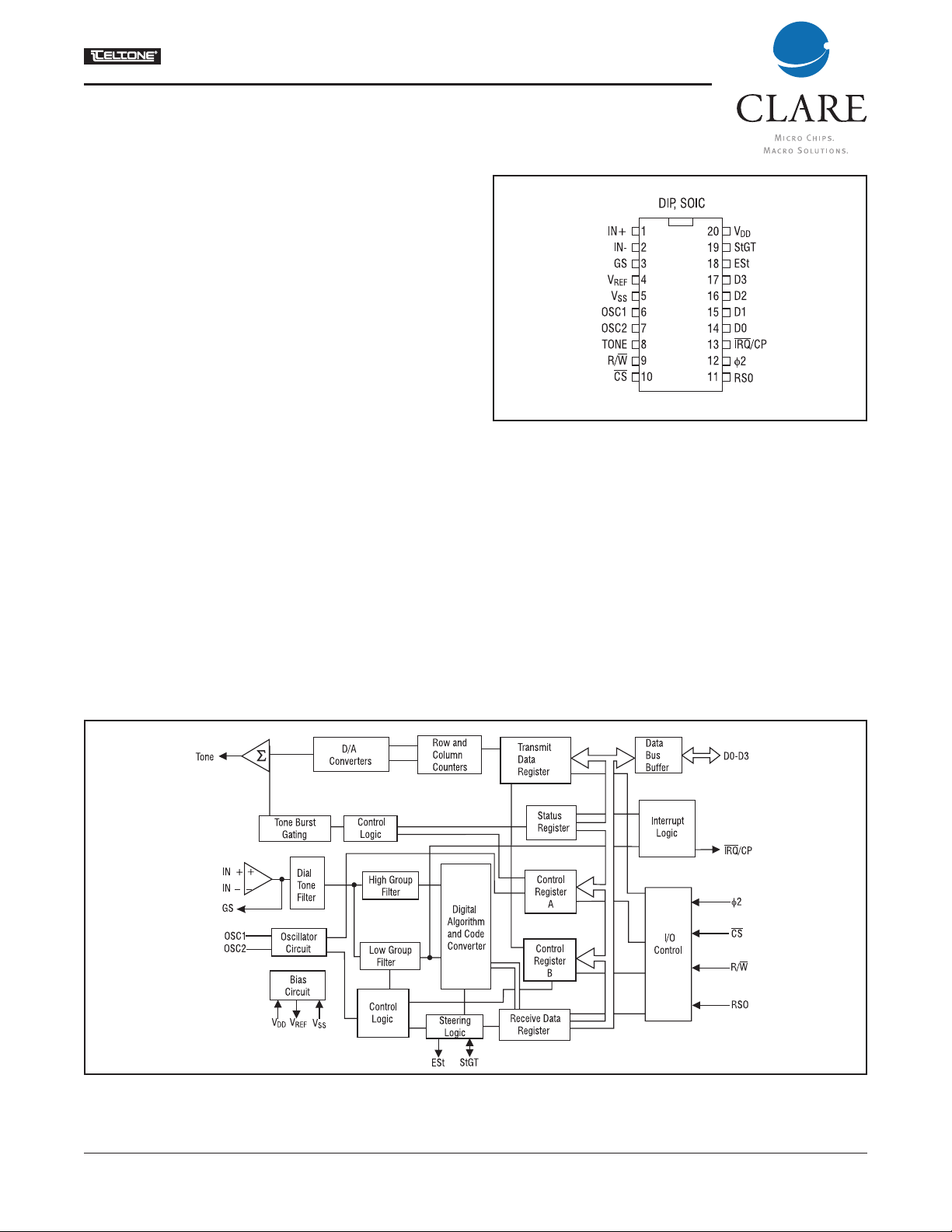
Figure 1 Pin Diagram
Functional Description
M-8880functionsconsistofahigh-performanceDTMFreceiver
withaninternalgainsettingamplifierandaDTMFgeneratorthat
containsatoneburstcounterforgeneratingprecisetonebursts
andpauses.Thecallprogressmode,whenselected,allowsthe
detectionofcallprogresstones.Astandard6500/6800series
microprocessorinterfaceallowsaccesstoaninternalstatus
register,twocontrolregisters,andtwodataregisters.
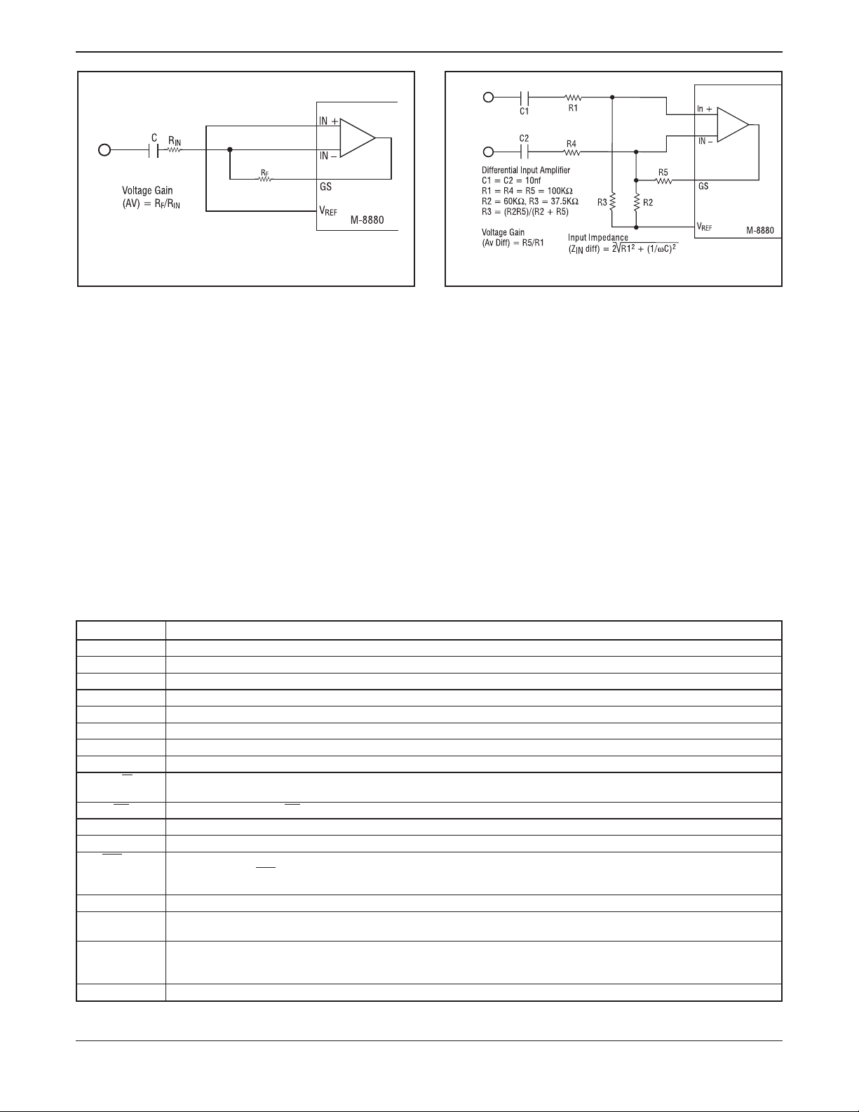
Input Configuration
Theinputarrangementconsistsofadifferentialinputoperationalamplifierandbiassources(V
inputsatV
feedbackresistortotheop-ampoutput(GS)forgainadjust
/2.Provisionsaremadefortheconnectionofa
DD
)forbiasingtheamplifier
REF
-
Figure 2 Block Diagram
40-406-00012, Rev. G www.clare.com
Page1
Page 2
M-8880
Figure 3 Single-Ended Input Configuration Figure 4 Differential Input Configuration
ment.Inasingle-endedconfiguration,theinputpinsshouldbe
connectedasshowninFigure3.Figure4showsthenecessary
connectionsforadifferentialinputconfiguration.
Receiver Section
Thelowandhighgrouptonesareseparatedbyapplyingthe
DTMFsignaltotheinputsoftwosixth-orderswitchedcapacitor
bandpassfilterswithbandwidthsthatcorrespondtothelowand
highgroupfrequencieslistedinTable2.Thelowgroupfilterin
corporatesnotchesat350and440Hz,providingexcellentdial
tonerejection.Eachfilteroutputisfollowedbyasingle-order
switchedcapacitorfilterthatsmoothsthesignalspriortolimiting.
Limitingisperformedbyhigh-gaincomparatorswithhysteresis
topreventdetectionofunwantedlow-levelsignals.Thecomparatoroutputsprovidefull-raillogicswingsattheincoming
DTMFsignalfrequencies.
Table 1 Pin Functions
Name Description
IN+
IN-
GS
V
REF
V
SS
OSC1
OSC2
TONE
R/W
CS
RS0
φ2
IRQ/CP
D0 - D3
ESt
St/GT
V
DD
Noninvertingop-amp input.
Inverting op-amp input.
Gain select. Gives access to output of front end differential amplifier for connection of feedback resistor.
Reference voltage output. NominallyVDD/2 is used to bias inputs at mid-rail.
Negative power supply input.
DTMF clock/oscillator input.
Clock output. A 3.5795 MHz crystal connected between OSC1 and OSC2 completes the internal oscillator circuit.
Dual tone multifrequency (DTMF) output.
Read/write input. Controls the direction of data transfer to and from the microprocessor and the receiver/transmitter.TTL
compatible.
Chip select.TTLinput (CS = 0 to select the chip).
Register select input. See Table 6.TTLcompatible.
System clock input. May be continuous orstrobedonly during read or write.TTLcompatible.
Interrupt request to microprocessor (open-drain output). Also, when call progress (CP) mode has been selected and inter
rupt enabled, theIRQ
op-amp. The input signal must be within the bandwidth limits of the call progress filter. See Figure 11
Microprocessor data bus.TTLcompatible.
Early steering output. Presents a logic high once the digital algorithm has detected a valid tone pair (signal condition). Any
momentary loss of signal condition will causeEStto return to a logic low.
Steering input/guard time output (bidirectional). A voltage greater thanV
detected tone pair and update the output latch. A voltage less thanV
GToutput acts to reset the external steering time-constant; its state is afuncitonofEStand the voltage on St.
Positive power supply input.
/CP pin will output a rectangular wave signal representative of the input signal applied at the input
Adecoderemploysdigitalcountingtechniquestodeterminethe
frequenciesoftheincomingtones,andtoverifythattheycorre
spondtostandardDTMFfrequencies.Acomplexaveragingal
gorithmprotectsagainsttonesimulationbyextraneoussignals
(suchasvoice),whiletoleratingsmalldeviationsinfrequency.
Thealgorithmprovidesanoptimumcombinationofimmunityto
talkoffwithtolerancetointerferingfrequencies(thirdtones)and
noise.Whenthedetectorrecognizesthepresenceoftwovalid
tones(referredtoas“signalcondition”),theearlysteering(ESt)
outputgoestoanactivestate.Anysubsequentlossofsignal
conditionwillcauseESttoassumeaninactivestate.
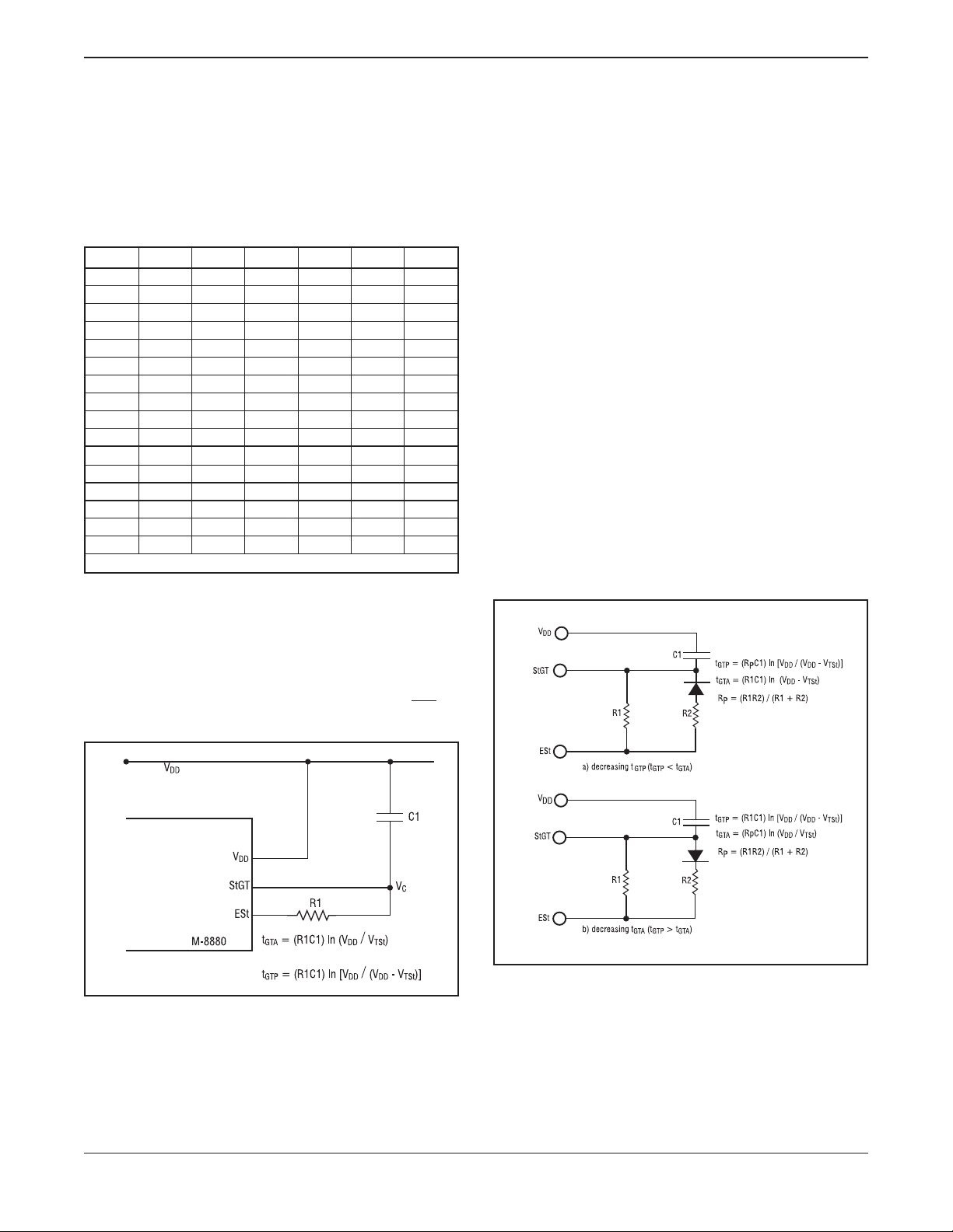
SteeringCircuit:Beforeadecodedtonepairisregistered,the
receiverchecksforavalidsignalduration(referredtoas“characterrecognitioncondition”).ThischeckisperformedbyanexternalRCtimeconstantdrivenbyESt.AlogichighonESt
-
detected at St causes the device to register the
TSt
frees the device to accept a new tone pair. The
TSt
-
-
40-406-00012, Rev. G www.clare.com
Page2
Page 3
M-8880
causesVC(seeFigure5)toriseasthecapacitordischarges.
Providedthatthesignalconditionismaintained(EStremains
high)forthevalidationperiod(t
(V
)ofthesteeringlogictoregisterthetonepair,latchingits
TSt
),VCreachesthethreshold
GTP
corresponding4-bitcode(seeTable2)intothereceivedatareg
ister.
Table 2 Tone Encoding/Decoding
F
697 1209 10001
697 1336 20010
697 1477 30011
770 1209 40100
770 1336 50101
770 1477 60110
852 1209 70111
852 1336 81000
852 1477 91001
941 1336 01010
941 1209
941 1477 #1100
697 1633 A 1101
770 1633 B 1110
852 1633 C 1111
941 1633 D 0000
F
LOW
0 = logic low, 1 = logic high
Digit D3 D2 D1 D0
HIGH
*
1011
Thesteeringcircuitworksinreversetovalidatetheinterdigit
pausebetweensignals.Thus,aswellasrejectingsignalstoo
shorttobeconsideredvalid,thereceiverwilltoleratesignalin
terruptions(dropout)tooshorttobeconsideredavalidpause.
Thiscapability,togetherwiththeabilitytoselectthesteering
-
timeconstantsexternally,allowsthedesignertotailorperfor
mancetomeetawidevarietyofsystemrequirements.
GuardTimeAdjustment:Thesimplesteeringcircuitshownin
Figure5isadequateformostapplications.Componentvalues
arechosenaccordingtotheformula:
t
REC=tDP+tGTP
TID=tDA+t
ThevalueoftDPisadeviceparameterandt
GTA
REC
signaldurationtoberecognizedbythereceiver.AvalueforC1
of0.1µFisrecommendedformostapplications,leavingR1to
beselectedbythedesigner.Differentsteeringarrangements
maybeusedtoselectindependentlytheguardtimesfortone
present(t
)andtoneabsent(t
GTP
).Thismaybenecessaryto
GTA
meetsystemspecificationsthatplacebothacceptandreject
limitsonbothtonedurationandinterdigitpause.Guardtimead
justmentalsoallowsthedesignertotailorsystemparameters
suchastalkoffandnoiseimmunity.Increasingt
talkoffperformancesinceitreducestheprobabilitythattones
simulatedbyspeechwillmaintainsignalconditionlongenough
toberegistered.Alternatively,arelativelyshortt
t
wouldbeappropriateforextremelynoisyenvironments
DO
wherefastacquisitiontimeandimmunitytotonedropoutsare
required.Designinformationforguardtimeadjustmentisshown
inFigure6.
istheminimum
improves
REC
withalong
REC
-
-
-
AtthispointtheStGToutputisactivatedanddrivesV
toVDD.
C
StGTcontinuestodrivehighaslongasEStremainshigh.
Finally,afterashortdelaytoallowtheoutputlatchtosettle,the
delayedsteeringoutputflaggoeshigh,signalingthatareceived
tonepairhasbeenregistered.Itispossibletomonitorthestatus
ofthedelayedsteeringflagbycheckingtheappropriatebitinthe
statusregister.Ifinterruptmodehasbeenselected,theIRQ
/CP
pinwillpulllowwhenthedelayedsteeringflagisactive.
Figure 5 Basic Steering Circuit
Thecontentsoftheoutputlatchareupdatedonanactivede
layedsteeringtransition.Thisdataispresentedtothe4-bit
bidirectionaldatabuswhenthereceivedataregisterisread.
Figure 6 Guard Time Adjustment
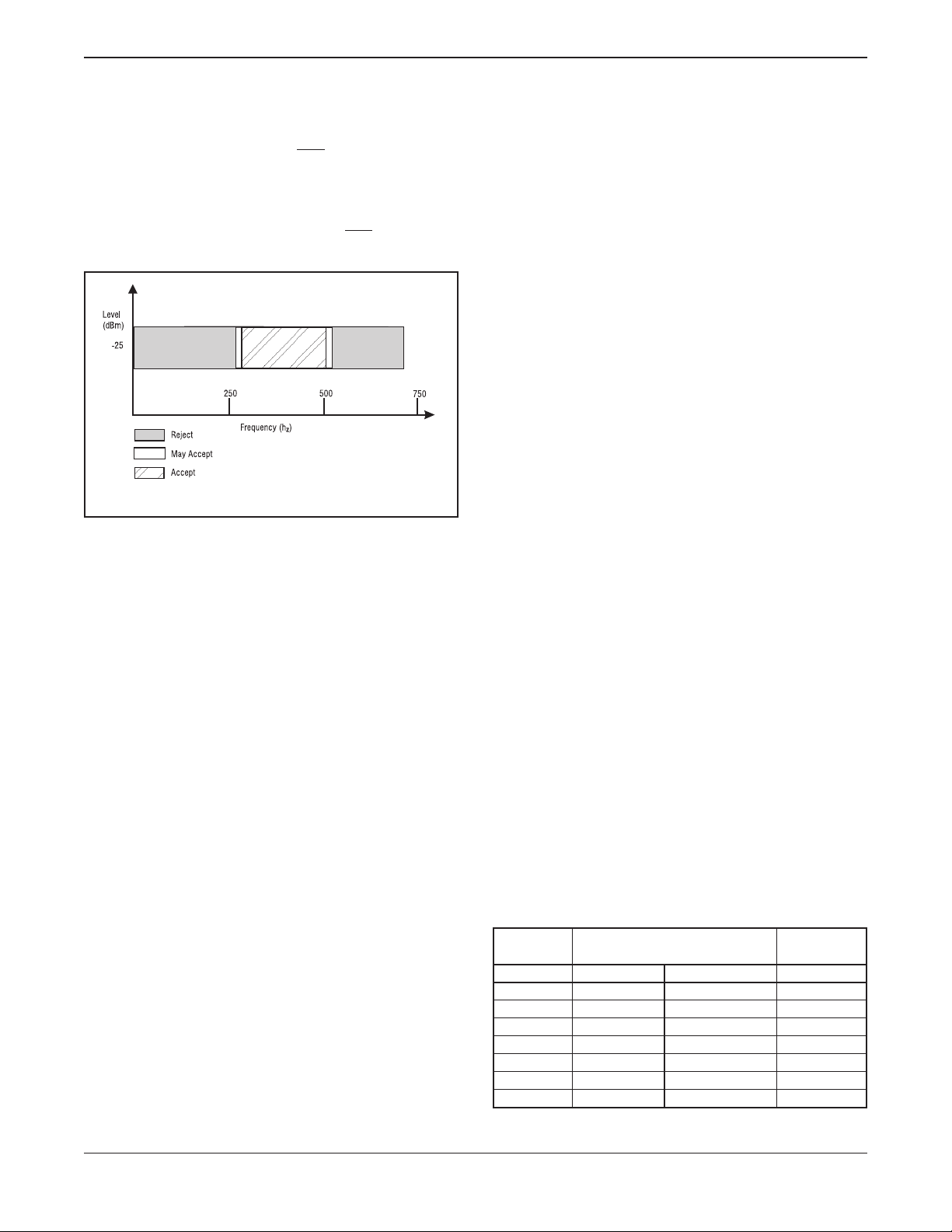
Call Progress Filter
Acallprogress(CP)modecanbeselected,allowingthedetec
tionofvarioustonesthatidentifytheprogressofatelephonecall
-
onthenetwork.ThecallprogresstoneinputandDTMFinputare
common;however,callprogresstonescanonlybedetected
whentheCPmodehasbeenselected.DTMFsignalscannotbe
-
40-406-00012, Rev. G www.clare.com
Page3
Page 4
M-8880
detectediftheCPmodehasbeenselected(seeTable3).Fig
ure7indicatestheusefuldetectbandwidthofthecallprogress
filter.Frequenciespresentedtotheinput(IN+andIN-)thatare
withinthe“accept”bandwidthlimitsofthefilterarehard-limited
byahigh-gaincomparatorwiththeIRQ
/CPpinservingasthe
output.Thesquarewaveoutputobtainedfromtheschmitttrig
gercanbeanalyzedbyamicroprocessororcounterarrange
menttodeterminethenatureofthecallprogresstonebeing
detected.Frequenciesinthe“reject”areawillnotbedetected,
andconsequentlytherewillbenoactivityonIRQ
/CPasaresult
ofthesefrequencies.
Figure 7 Call Progress Response
DTMF Generator
TheDTMFtransmitterusedintheM-8880iscapableofgeneratingall16standardDTMFtonepairswithlowdistortionandhigh
accuracy.Allfrequenciesarederivedfromanexternal3.58
MHzcrystal.Thesinusoidalwaveformsfortheindividualtones
aredigitallysynthesizedusingrowandcolumnprogrammable
dividersandswitchedcapacitordigital-to-analogconverters.
Therowandcolumntonesaremixedandfiltered,providinga
DTMFsignalwithlowtotalharmonicdistortionandhighaccu
racy.TospecifyaDTMFsignal,dataconformingtotheencod
ingformatshowninTable2mustbewrittentothetransmitdata
register.Notethatthisisthesameasthereceiveroutputcode.
Theindividualtonesthataregenerated(f
LOW
andf
HIGH
)arere
ferredtoaslow-groupandhigh-grouptones.Typically,the
high-grouptolow-groupamplituderatio(twist)is2dBtocom
pensateforhigh-groupattenuationonlongloops.
Operation:Duringwriteoperationstothetransmitdataregister,
4-bitdataonthebusislatchedandconvertedtoa2of8codefor
usebytheprogrammabledividercircuitrytospecifyatimeseg
mentlengththatwillultimatelydeterminethetonefrequency.
Thenumberoftimesegmentsisfixedat32,butthefrequencyis
variedbyvaryingthesegmentlength.Whenthedividerreaches
theappropriatecountasdeterminedbytheinputcode,areset
pulseisissuedandthecounterstartsagain.Thedivideroutput
clocksanothercounterthataddressesthesinewavelookup
ROM.Thelookuptablecontainscodesusedbytheswitched
capacitorD/Aconvertertoobtaindiscreteandhighlyaccurate
DCvoltagelevels.Twoidenticalcircuitsareusedtoproduce
rowandcolumntones,whicharethenmixedusingalow-noise
summingamplifier.Theoscillatordescribedneedsno“startup”
timeasinotherDTMFgenerators,sincethecrystaloscillatoris
runningcontinuously,thusprovidingahighdegreeoftoneburst
accuracy.Whenthereisnotoneoutputsignal,theTONEpin
assumesaDClevelof2.5volts(typically).Abandwidthlimiting
filterisincorporatedtoattenuatedistortionproductsabove4
KHz.
BurstMode:Certaintelephonyapplicationsrequirethatgener
atedDTMFsignalsbeofaspecificduration,determinedeither
bytheapplicationorbyanyoftheexistingexchangetransmitter
specifications.StandardDTMFsignaltimingcanbeaccom
plishedbymakinguseoftheburstmode.Thetransmitterisca
pableofissuingsymmetricbursts/pausesofpredetermined
duration.Thisburst/pausedurationis51ms±1ms,astandard
intervalforautodialerandcentralofficeapplications.Afterthe
burst/pausehasbeenissued,theappropriatebitissetinthesta
tusregister,indicatingthatthetransmitterisreadyformoredata.
ThetimingdescribedisavailablewhentheDTMFmodehas
beenselected.However,whencallprogress(CP)modeisse
lected,asecondaryburst/pausetimeisavailablethatextends
thisintervalto102ms±2ms.Theextendedintervalisuseful
whenprecisetoneburstsoflongerthan51msdurationand51
mspausearedesired.NotethatwhenCPmodeandburstmode
havebeenselected,DTMFtonesmaybetransmittedonlyand
not
received.Inapplicationsrequiringanonstandard
burst/pausetime,useasoftwaretiminglooporexternaltimer.
Thisprovidesthetimingpulseswhentheburstmodeisdisabled
byenablinganddisablingthetransmitter.
TheM-8880isinitializedonpowerupsequencewithDTMF
modeandburstmodeselected.
Single-ToneGeneration:Asingle-tonemodeisavailable
wherebyindividualtonesfromthelowgrouporhighgroupcan
begenerated.ThismodecanbeusedforDTMFtestequipment
applications,acknowledgmenttonegeneration,anddistortion
measurements.RefertoTable4fordetails.
DistortionCalculations:TheM-8880iscapableofproducing
precisetoneburstswithminimalerrorinfrequency(seeTable
-
3).Theinternalsummingamplifierisfollowedbyafirst-order
-
low-passswitchedcapacitorfiltertominimizeharmoniccompo
nentsandintermodulationproducts.Thetotalharmonicdistor
single
tionfora
-
Figure9)whichistheratioofthetotalpowerofalltheextrane
ousfrequenciestothepowerofthefundamentalfrequencyex
-
pressedasapercentage.TheFouriercomponentsofthetone
tone can be calculated using Equation 1, (see
outputcorrespondtoV2f...Vnfasmeasuredontheoutput
waveform.Thetotalharmonicdistortionfora
dual
calculatedusingEquation2(seeFigure9).
-
Table 3 Actual Frequencies vs. Standard
Requirements
Active
Cell
L1 697 699.1 + 0.30
L2 770 766.2 - 0.49
L3 852 847.4 - 0.54
L4 941 948.0 + 0.74
H1 1209 1215.9 + 0.57
H2 1336 1331.7 - 0.32
H3 1447 1471.9 - 0.35
H4 1633 1645.0 + 0.73
Output Frequency (Hz)
Specified Actual
-
-
-
-
-
-
-
-
-
tone can be
% Error
40-406-00012, Rev. G www.clare.com
Page4
Page 5
M-8880
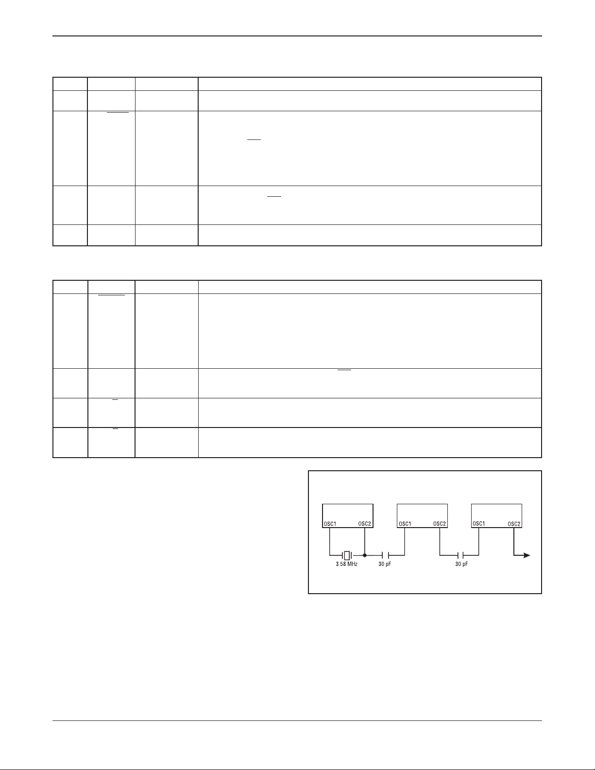
Table 4 Control Register A Description
Bit Name Function Description
b0 TOUT Tone output
b1 CP/DTMF Mode control
b2 IRQ Interrupt enable
b3 RSET Register select
Bit Name Function Description
b0 BURST Burst mode
b1 TEST Test mode
b2 S/D Single/dual tone
generation
b3 C/R Column/row
tones
A logic 1 enables the tone output. This function can be implemented in either the burst mode or
nonburstmode.
In DTMF mode (logic 0), the device is capable of generating and receiving DTMF signals. When
the call progress (CP) mode is selected (logic 1), a 6th-order bandpass filter is enabled to allow
call progress tones to be detected. Call progress tones within the specified bandwidth will be pre
sented at theIRQ
when the CP mode and burst mode have both been selected, the transmitter will issue DTMF sig
nals with a burst and pause of 102 ms (typ) duration. This signal duration is twice that obtained
from the DTMF transmitter, if DTMF mode had been selected. Note that DTMF signals cannot be
decoded when the CP mode has been selected.
A logic 1 enables the interrupt mode. When this mode is active and the DTMF mode has been se
lected (b1= 0), theIRQ
has been received and has been present for the guard time or (2) the transmitter is ready for more
data (burst mode only).
A logic 1 selects control register B on the next write cycle to the control register address. Subse
quent write cycles to the control register are directed back to control register A.
/CP pin in rectangular wave format if theIRQbit has been enabled (b2=1). Also,
/CP pin will pull to a logic 0 condition when either (1) a valid DTMF signal
Table 5 Control Register B Description
A logic 0 enables the burst mode. When this mode is selected, data corresponding to the desired
DTMF tone pair can be written to the transmit data register, resulting in a tone burst of a specific
duration (see Table 12). Subsequently, a pause of the same duration is induced. Immediately fol
lowing the pause, the status register is updated indicating that the transmit data register is ready
for further instructions, and an interrupt will be generated if the interrupt mode has been enabled.
Additionally, if call progress (CP) mode has been enabled, the burst and pause duration isincreed
by a factor of two. When the burst mode is not selected (logic 1), tone bursts of any desired duration may be generated.
By enabling the test mode (logic 1), theIRQ/CP pin will present the delayed steering (inverted)
signal from the DTMF receiver. Refer to Figure 11 (b3 waveform) for details concerning the output
waveform. DTMF mode must be selected (CRAb1= 0) before test mode can be implemented.
A logic 0 will allow DTMF signals to be produced. If single-tone generation is enabled (logic 1), either now or column tones (low or high group) can be generated depending on the state of b3 in
control register B.
When used in conjunction withb2(above), the transmitter can be made to generate single-row or
single-column frequencies. A logic0 will select row frequencies and a logic 1 will select column fre
quencies.
-
-
-
-
-
-
VLandVHcorrespondtothelow-groupandhigh-groupampli
tude,respectively,andV
2
isthesumofalltheintermodulation
IMD
-
components.Theinternalswitchedcapacitorfilterfollowingthe
D/Aconverterkeepsdistortionproductsdowntoaverylow
level.
DTMF Clock Circuit
Theinternalclockcircuitiscompletedwiththeadditionofastan
dard3.579545MHztelevisioncolorburstcrystal.Anumberof
M-8880devicescanbeconnectedasshowninFigure8using
onlyonecrystal.
Microprocessor Interface
TheM-8880usesamicroprocessorinterfacethatallowspre
-
Figure 8 Common Crystal Connection
cisecontroloftransmitterandreceiverfunctions.Fiveinternal
registersareassociatedwiththemicroprocessorinterface,
whichcanbesubdividedintothreecategories:datatransfer,
transceivercontrol,andtransceiverstatus.Tworegistersare
associatedwithdatatransferoperations.Thereceivedata,
read-only,containstheoutputcodeofthelastvalidDTMFtone
pairtobedecoded.Thedataenteredinthetransmitdataregis
terdetermineswhichtonepairistobegenerated(seeTable2).
40-406-00012, Rev. G www.clare.com
Datacanonlybewrittentothetransmitdataregister.Trans
ceivercontrolisaccomplishedwithtwocontrolregisters(CRA
andCRB),occupyingthesameaddressspace.Awriteopera
tiontoCRBcanbeexecutedbysettingtheappropriatebitin
CRA.Thefollowingwriteoperationtothesameaddresswill
-
thenbedirectedtoCRB,andsubsequentwritecycleswillthen
beredirectedtoCRA.Internalresetcircuitryclearsthecontrol
Page5
-
-
Page 6
registersonpowerup;however,asaprecautionarymeasurethe
initializationsoftwareshouldincludearoutinetocleartheregis
ters.RefertoTables3and4fordetailsonthecontrolregisters.
TheIRQ
/CPpincanbeprogrammedtoprovideaninterruptre
questsignalonvalidationofDTMFsignals,orwhenthetrans
mitterisreadyformoredata(burstmodeonly).TheIRQ
/CPpin
isconfiguredasanopen-drainoutputdeviceandassuchre
quiresapullupresistor(seeFigure10).
Ordering Information
M-888001P 20-pin plastic DIP
M-8880-01SM 20-pin plasticSOIC
M-8880-01T 20-pin plasticSOIC,Tape and Reel
M-8880
-
-
-
-
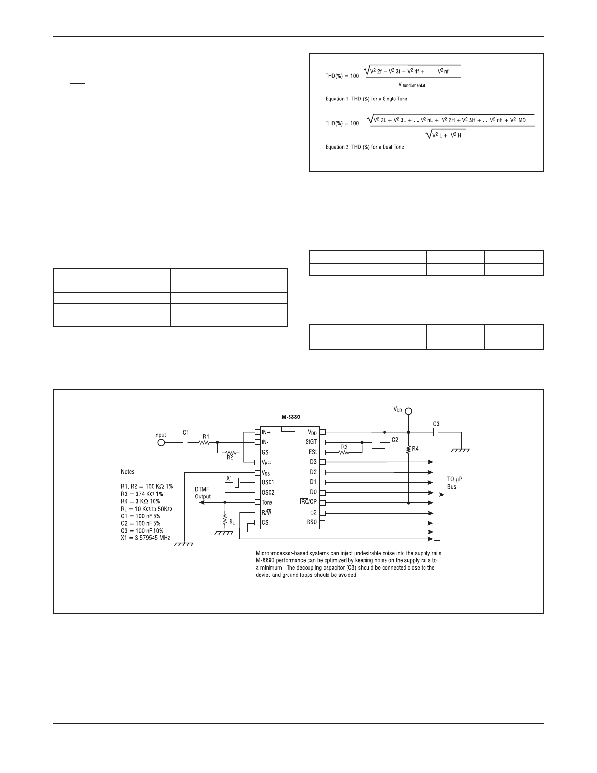
Figure 9 Equations
Table 7CRABitPostions
Table 6 Internal Register Functions
RS0 R/W Function
0 0 Write to transmitter
0 1 Read from receiver
1 0 Write to control register
1 1 Read from status register
b3 b2 b1 b0
RSEL IRQ CP/DTMF TOUT
Table 8CRBBit Positions
b3 b2 b1 b0
C/R S/D TEST BURST
Figure 10 Application Circuit (Single-Ended Input)
40-406-00012, Rev. G www.clare.com
Page6
Page 7
M-8880
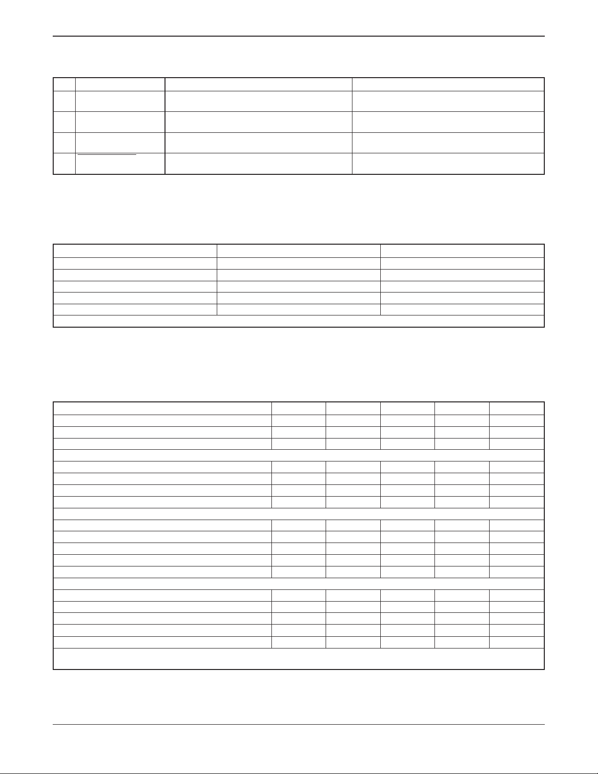
Table 9 Status Register Description
BIT Name Status Flag Set Status Flag Cleared
b0
IRQ Interrupt has occurred. Bi tone (b1) and/or bit 2 (b2)
is set.
b1
Transmit data register
empty (burst mode only)
b2
Receive data register
Pause duration has terminated and transmitter is
ready for new data.
Valid data is in the receive data register. Cleared after status register is read.
full
b3
Delayed steering Set on valid detection of the absence of a DTMF sig
nal.
Table 10 Absolute Maximum Ratings
Parameter Symbol Value
Power supply voltage (VDD-VSS)
Voltage on any pin
Current on any pin
Operating temperature
Storage temperature
Note:Exceeding these ratings may cause permanent damage. Functional operation under these conditions is not implied.
V
DD
V
dc
I
DD
T
A
T
S
Interrupt is inactive. Cleared after status register is
read.
Cleared after status register is read or when not in
burst mode.
Cleared on detection of a valid DTMF signal.
-
+ 6.0 V max
VSS-0.3 V toVDD+ 0.3 V
10 mA max
-40°C to +85°C
-65°C to +150°C
Table 11 DC Characteristics
Parameter Symbol Min Typ* Max Units
Operating supply voltage
Operating supply current
Power consumption
V
DD
I
DD
P
O
Inputs
High-level input voltage, OSC1
Low-level input voltage, OSC1
Input impedance (@ 1 kHz), IN+, INSteering threshold voltage
V
IHO
V
ILO
R
IN
V
TSt
Outputs
High-level output voltage (no load), OSC2
Low-level output voltage (no load), OSC2
Output leakage current (V
V
output voltage (no load)
REF
output resistance
V
REF
= 2.4V),IRQ
OH
V
V
V
OHO
OLO
I
OZ
REF
R
OR
Data Bus
Low-level input voltage
High-level input voltage
Low-level output voltage (I
High-level output voltage (I
Input leakage current (V
All voltages referenced toV
= 1.6 mA)
OL
= 400µA)
OH
= 0.4 to 2.4 V)
IN
unless otherwise noted.VDD= 5.0 V±5%;fC= 3.579545MHz;ΤA= -40°C to +85°C, unless otherwise
SS
V
IL
V
IH
V
OL
V
OH
I
IZ
noted. *Typical values are for use as design aids only, and are not guaranteed or subject to production testing.
4.75 5.0 5.25 V
—1015mA
— 50 78.75 mW
3.5 — — V
— — 1.5 V
—10—
2.2 2.3 2.5 V
VDD- 0.1V — — V
— — 0.1 V
— 1.0 10.0
2.4 — 2.7 V
— 1.0
— — 0.8 V
2.0 — — V
— — 0.4 V
2.4 — — V
— — 10.0
MΩ
µA
kΩ
µA
40-406-00012, Rev. G www.clare.com
Page7
Page 8
M-8880
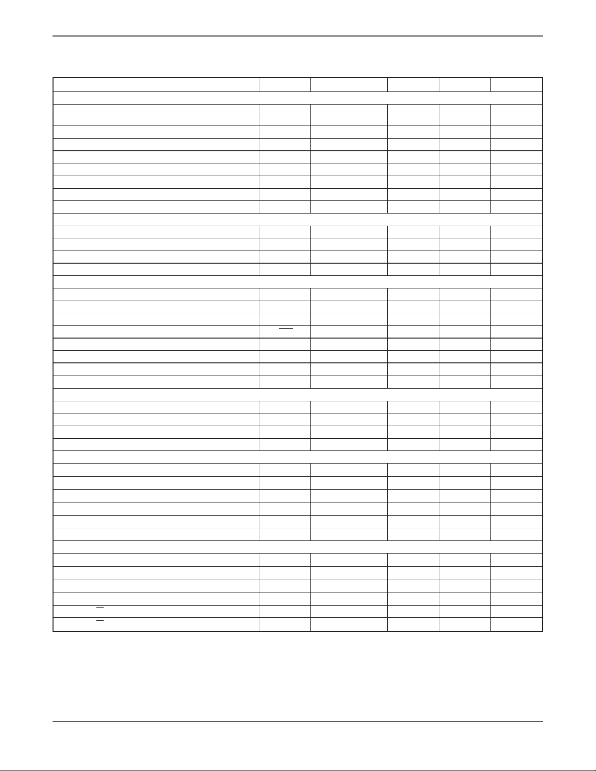
Table 12 AC Characteristics
PARAMETER SYMBOL MIN TYP* MAX UNITS
Receive signal conditions
Valid input signal levels
(each tone of composite signal; Notes 1, 2, 3, 5, 6, 9)
Positive twist accept (Notes 2, 3, 6, 9)
Negative twist accept (Notes 2, 3, 6, 9)
Frequency deviation accept (Notes 2, 3, 5, 9)
Frequency deviation reject (Notes 2, 3, 5)
Third tone tolerance (Notes 2, 3, 4, 5, 9, 10)
Noise tolerance (Notes 2, 3, 4, 5, 7, 9, 10)
Dial tone tolerance (Notes 2, 3, 4, 5, 8, 9, 11)
Call progress
Lower frequency (@ -25 dBm) accept
Upper frequency (@ -25 dBm) accept
Lower frequency (@ -25 dBm) reject
Upper frequency (@ -25 dBm) reject
f
LA
f
HA
f
LR
f
HR
Receive timing
Tone present detect time
Tone absent detect time
Tone duration accept (ref. Figure 12)
Tone duration reject (ref. Figure 12)
Interdigitpause accept (ref. Figure 12)
Interdigitpause reject (ref. Figure 12)
Delay St to b3
Delay St toRX
—RX
O
3
t
DP
t
DA
t
REC
t
REC
t
t
DO
t
PStb3
t
PStRX
ID
Transmit timing
Tone burst duration (DTMF mode)
Tone pause duration (DTMF mode)
Tone burst duration (extended, call progress mode)
Tone pause duration (extended, call progress mode)
t
BST
t
PS
t
BSTE
t
PSE
Tone output
High group output level (R
Low group output level (R
Pre-emphasis (R
= 10 kW)
L
Output distortion (R
= 10 kΩ)
L
= 10 kW)
L
= 10 kΩ, 3.4 kHz bandwidth)
L
Frequency deviation (f = 3.5795 MHz)
Output load resistance
V
HOUT
V
LOUT
dB
P
THD — -25 — dB
f
D
R
LT
Microprocessor interface
φ2 cycle period
φ2 high pulse width
φ2 low pulse width
φ2 rise and fall time
Address, R/W
Address, R/W
hold time
setup time (prior toφ2)
t
CYC
t
CH
t
CL
t
R,tF
tAH,t
RWH
t
AS,tRWS
± 1.5%± 2 Hz — — Nom.
±3.5%
-29
27.5
—
—
+1
869
mV
dBm
RMS
—6dB
—6dB
— — Nom.
— -16 — dB
— -12 — dB
— +22 — dB
— 320 — Hz
— 510 — Hz
— 290 — Hz
— 540 — Hz
51114ms
0.5 4 8.5 ms
— — 40 ms
20 — — ms
— — 40 ms
20 — — ms
—13—
—8—
µs
µs
50 — 52 ms
50 — 52 ms
100 — 104 ms
100 — 104 ms
-6.1 — -2.1 dBm
-8.1 — -4.1 dBm
023dB
— ± 0.7 ± 1.5 %
10 — 50
0.5 — —
kΩ
µs
200 — — ns
180 — ns
— — 25 ns
10 — — ns
23 — — ns
40-406-00012, Rev. G www.clare.com
Page8
Page 9
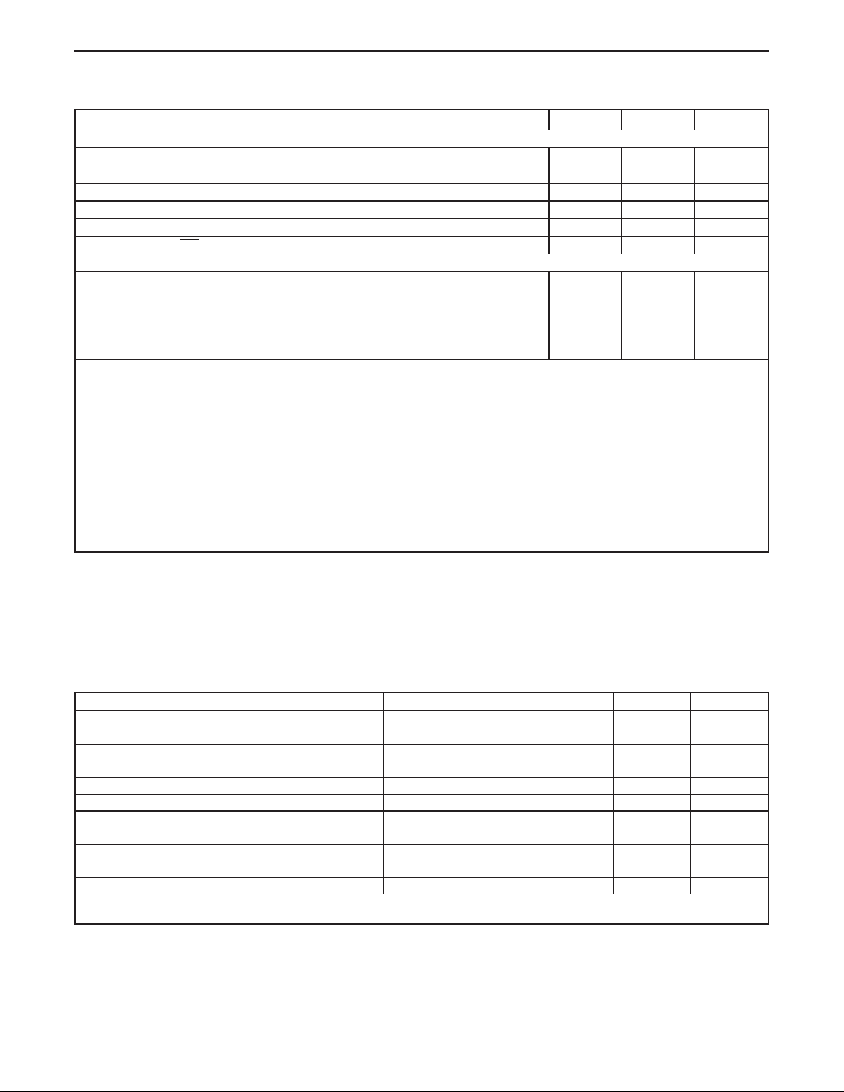
M-8880
Table 12 AC Characteristics (continued)
Parameter Symbol Min Typ* Max Units
Microprocessor interface (continued)
Data hold time (read)
f2 to valid data delay (read) (200 pF load)
Data setup time (write)
Data hold time (write)
Input capacitance, D0—D3
Output capacitance,IRQ/CP
t
DHR
t
DDR
t
DSW
t
DHW
C
IN
C/
OUT
DTMF clock
t
LHCL
t
HLCL
DC
C
f
C
CL
LO
Crystal clock frequency
Clock input rise time (external clock)
Clock input fall time (external clock)
Clock input duty cycle (external clock)
Capacitive load, OSC2
All voltages referenced to unless otherwise noted.VDD= 5.0 V±5%;VSS= 0 V;fC= 3.579545 MHz; TA= -40°C to +85°C
*Typical values are for use as design aids only, and are not guaranteed or subject to production testing.
Notes:
1. dBm = decibels above or below a reference power of 1mWinto a 600Wload.
2. Digit sequence consists of all 16 DTMF tones.
3. Tone duration = 40 ms. Tone pause = 40 ms.
4. Nominal DTMF frequencies are used.
5. Both tones in the composite signal have an equal amplitude.
6. The tone pair is deviated by±1.5%±2 Hz.
7. Bandwidth limited (3 kHz)Gaussiannoise.
8. The precise dial tone frequencies are 350 and 440 Hz (±2%).
9. For an error rate of less than 1 in 10,000.
10. Referenced to the lowest amplitude tone in the DTMF signal.
11. Referenced to the minimum valid accept level.
22 — — ns
— — 150 ns
45 — — ns
10 — — ns
—5—pF
—5—pF
3.5759 3.5795 3.5831 MHz
— — 110 ns
— — 110 ns
40 50 60 %
— — 30 pF
Table 13 Electrical Characteristics - Gain Setting Amplifier
Parameter Symbol Min Typ* Max Units
Input leakage current (V
SS£VIN£VDD
)
Input resistance
Input offset voltage
Power supply rejection (1 KHz)
Common mode rejection (-3.0 V£V
IN
£3.0 V
)
DC open-loop voltage gain
Unity gain bandwidth
Output voltage swing (R
³100 KΩtoVSS)
L
Maximum capacitive load, GS
Maximum resistive load, GS
Common mode range (no load)
I
IN
R
IN
V
OS
PSRR — 60 — dB
CMRR — 60 — dB
A
VOL
BW — 1.5 — MHz
V
O
C
L
R
L
V
CM
— 100 — nA
—10—
MΩ
—25—mV
—65—dB
— 4.5 — V
PP
— 100 — pF
—50—
— 3.0 — V
KΩ
PP
All voltages referenced tounless otherwise noted.VDD= 5.0 V;VSS= 0 V; TA= 25°C
*Typical values are for use as design aids only, and are not guaranteed or subject to production testing.
40-406-00012, Rev. G www.clare.com
Page9
Page 10
M-8880
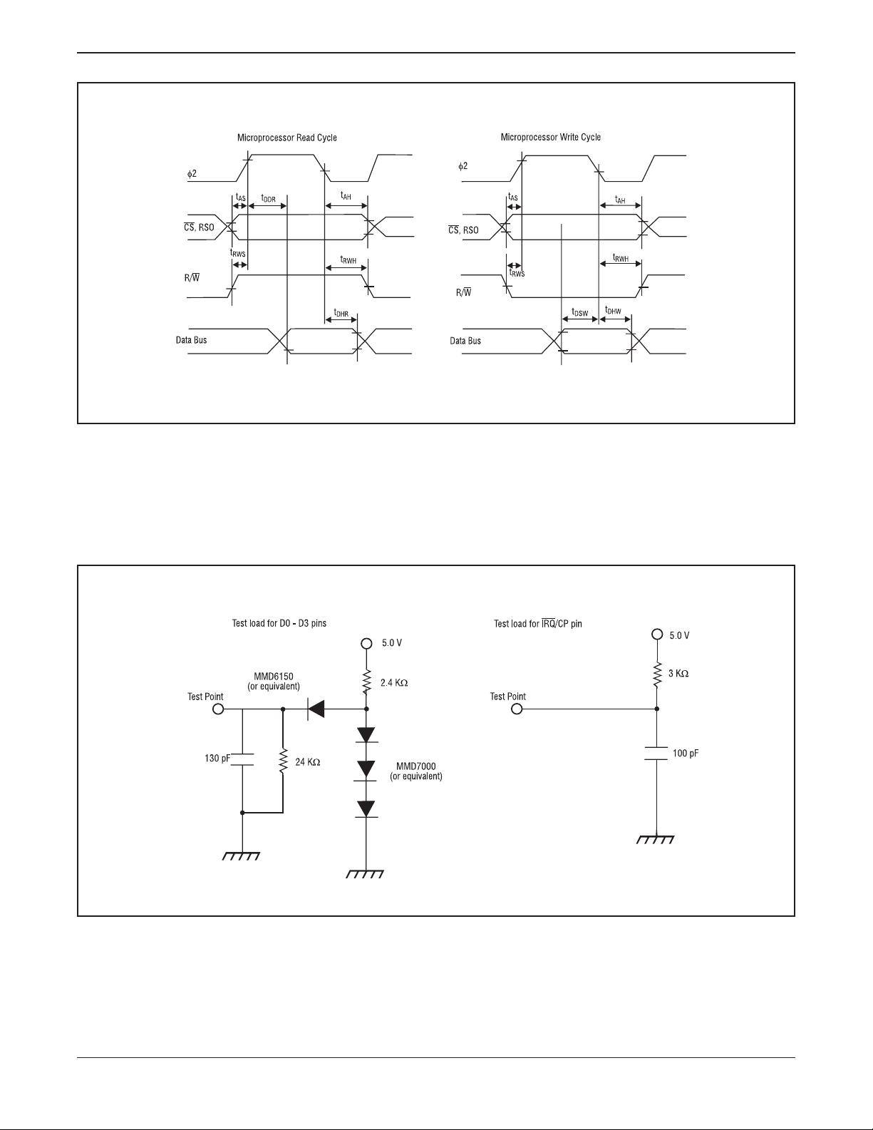
Figure 11 Timing Diagrams
Figure 12 Test Loads
40-406-00012, Rev. G www.clare.com
Page10
Page 11
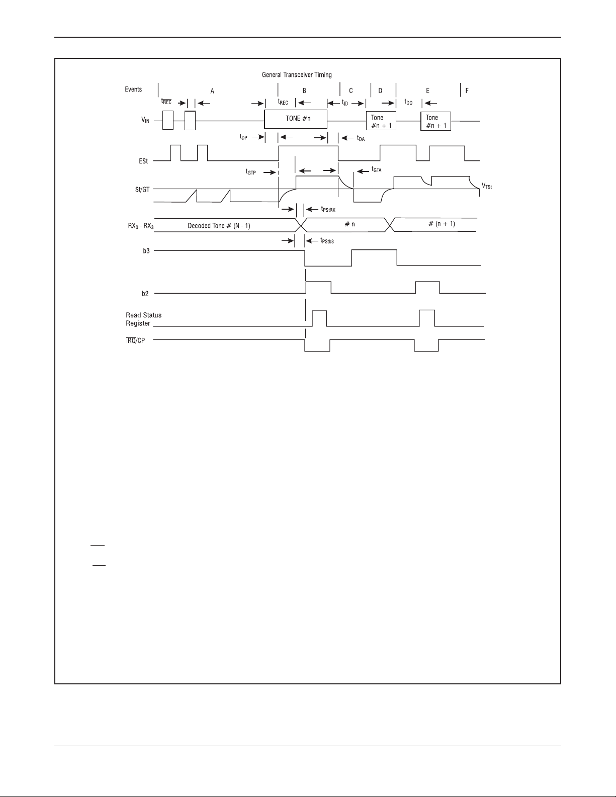
M-8880
Explanation of Events
(A) Tone bursts detected, tone duration invalid,RXData Register not updated.
(B) Tone #n detected, tone duration valid, tone decoded and latched inRXData Register.
(C) End of tone #n detected, tone absent duration valid,RXData Register remain latched until next valid tone.
(D) Tone #n + 1 detected, tone duration valid, tone decoded and latched inRXData Register.
(E) Acceptable dropout of tone #n + 1, tone absent duration invalid,RXData Register remain latched.
(F) End of tone #n + 1 detected, tone absent duration valid,RXData Register remain latched until next valid tone.
Explanation of Symbols
V
IN
DTMF composite input signal.
ESt Early steering output. Indicates detection of valid tone frequencies.
St/GT Steering input/guard time output. Drives external RC timing circuit.
RX
-RX
0
3
b3 Delayed steering output. Indicates that valid frequencies have been present/absent for the
4-bit decoded data in receive data register.
required guard time, thus constituting a valid DTMF signal.
b2 Output enable (input). A low level shifts Q1 - Q4 to its high impedance state.
/CP Interrupt is active indicating that new data is in theRXdata register. The interrupt is cleared
IRQ
t
REC
t
REC
t
ID
t
DO
t
DP
t
DA
T
GTP
t
GTA
after the status register is ready.
Maximum DTMF signal duration not detected as valid.
Minimum DTMF signal duration required for valid recognition.
Minimum time between valid DTMF signals.
Maximum allowable dropout during valid DTMF signal.
Time to detect the presence of valid DTMF signals.
Time to detect the absence of valid DTMF signals.
Guard time, tone present.
Guard time, tone absent.
Figure 13 Timing Diagrams
40-406-00012, Rev. G www.clare.com
Page11
Page 12
M-8880
Tolerances
Inches Metric (mm)
Min Max Min Max
A .210 5.33
A1 .015 .38
b .014 .022 .36 .56
2 .045 .070 1.14 1.78
b
C .008 .014 .20 .36
D .980 1.060 24.89 26.92
E .300 .325 7.62 8.26
E1 .240 .280 6.10 7.11
e .100BSC 2.54BSC
c
e
L .115 .150 2.92 3.81
A .093 .104 2.35 2.65
A1 .004 .012 .10 .30
b .013 .020 .33 .51
D .496 .512 12.60 13.00
E .291 .299 7.39 7.59
e .050BSC 1.27BSC
H .394 .419 10.00 10.65
L .016 .050 .40 1.27
15° 0° 15°
0°
Tolerances
Inches Metric (mm)
Min Max Min Max
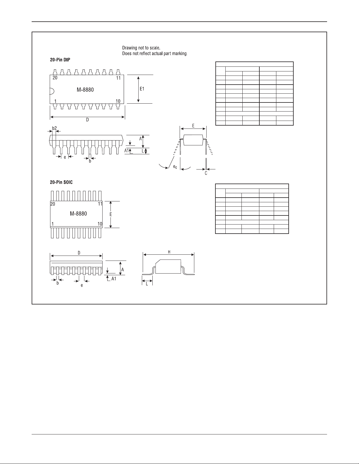
Figure 14 Package Dimensions
40-406-00012, Rev. G www.clare.com
Page12
Page 13

Worldwide Sales Offices
CLARE LOCATIONS
Clare Headquarters
78 Cherry Hill Drive
Beverly, MA 01915
Tel: 1-978-524-6700
Fax: 1-978-524-4900
Toll Free: 1-800-27-CLARE
Clare Micronix Division
145 Columbia
Aliso Viejo, CA 92656-1490
Tel: 1-949-831-4622
Fax: 1-949-831-4628
SALES OFFICES
AMERICAS
Americas Headquarters
Clare
78 Cherry Hill Drive
Beverly, MA 01915
Tel: 1-978-524-6700
Fax: 1-978-524-4900
Toll Free: 1-800-27-CLARE
Eastern Region
Clare
P.O. Box 856
Mahwah, NJ 07430
Tel: 1-201-236-0101
Fax: 1-201-236-8685
Toll Free: 1-800-27-CLARE
Central Region
Clare Canada Ltd.
3425 Harvester Road, Suite 202
Burlington, Ontario L7N 3N1
Tel: 1-905-333-9066
Fax: 1-905-333-1824
EUROPE
European Headquarters
CP Clare nv
Bampslaan 17
B-3500 Hasselt (Belgium)
Tel: 32-11-300868
Fax: 32-11-300890
France
Clare France Sales
Lead Rep
99 route de Versailles
91160 Champlan
France
Tel: 33 1 69 79 93 50
Fax: 33 1 69 79 93 59
Germany
Clare Germany Sales
ActiveComp Electronic GmbH
Mitterstrasse 12
85077 Manching
Germany
Tel: 49 8459 3214 10
Fax: 49 8459 3214 29
Italy
C.L.A.R.E.s.a.s.
Via C. Colombo 10/A
I-20066 Melzo (Milano)
Tel: 39-02-95737160
Fax: 39-02-95738829
Sweden
Clare Sales
Comptronic AB
Box 167
S-16329 Spånga
Tel: 46-862-10370
Fax: 46-862-10371
ASIA PACIFIC
Asian Headquarters
Clare
Room N1016, Chia-Hsin, Bldg II,
10F, No. 96, Sec. 2
Chung Shan North Road
Taipei, Taiwan R.O.C.
Tel: 886-2-2523-6368
Fax: 886-2-2523-6369
http://www.clare.com
Northwestern Region
Clare
1852 West 11th Street, #348
Tracy, CA 95376
Tel: 1-209-832-4367
Fax: 1-209-832-4732
Toll Free: 1-800-27-CLARE
Southwestern Region
Clare
2816 Nevis Circle
Costa Mesa, CA 92626
Tel: 1-714-556-3661
Fax: 1-714-546-4254
Toll Free: 1-800-27-CLARE
Canada
Clare Canada Ltd.
3425 Harvester Road, Suite 202
Burlington, Ontario L7N 3N1
Tel: 1-905-333-9066
Fax: 1-905-333-1824
United Kingdom
Clare UK Sales
Marco Polo House
Cook Way
Bindon Road
Taunton
UK-Somerset TA2 6BG
Tel: 44-1-823 352541
Fax: 44-1-823 352797
Clare cannot assume responsibility for use of any circuitry other then circuitry entirely embodied in this Clare product. No circuit patent licenses nor
indemnity are expressed or implied. Clare reserves the right to change the
specification and circuitry, without notice at an y time. The products described in this document are not intended for use in medical implantation
or other direct life support applications where malfunction may result in
direct physical harm, injury or death to a person.
Specification: 40-406-00012, Rev. G
© Copyright 2000, CP Clare Corporation d/b/a Clare
All rights reserved. Printed in USA.
07/28/00
 Loading...