

Datasheet M8813F2W, M8834F2W, M8813F2Y, M8813F1Y, M8813F1W Datasheet (SGS Thomson Microelectronics)
...Page 1
In-System Programmable (ISP) Multiple-Memory and
Logic FLASH+PSD Systems (with CPLD) for MCUs
■ Single Supply Voltage:
–5V±10% for M88xxFxY
– 3 V (+20/–10%) for M88xxFxW
■ 1 or 2 Mbit of Primary Flash Memory (8 uniform
sectors, 16K x 8, or 32K x 8)
■ A second non-volatile memory:
– 256 Kbit (32K x 8) EEPROM (for M8813F1x)
or Flash memory (for M88x3F2x)
– 4 uniform sectors (8K x 8)
■ SRAM (16 Kbit, 2K x 8; or 64 Kbit, 8K x 8)
■ Over 3,000 Gates of PLD: DPLD and CPLD
■ 27 Reconfigurable I/O ports
■ Enhanced JTAGSerial Port
■ Programmable power management
■ Stand-by current:
–50µA for M88xxFxY
–25µA for M88xxFxW
■ High Endurance:
– 100,000 Erase/Write Cycles of FlashMemory
– 10,000 Erase/Write Cycles of EEPROM
– 1,000 Erase/Write Cycles of PLD
M88 FAMILY
DATA BRIEFING
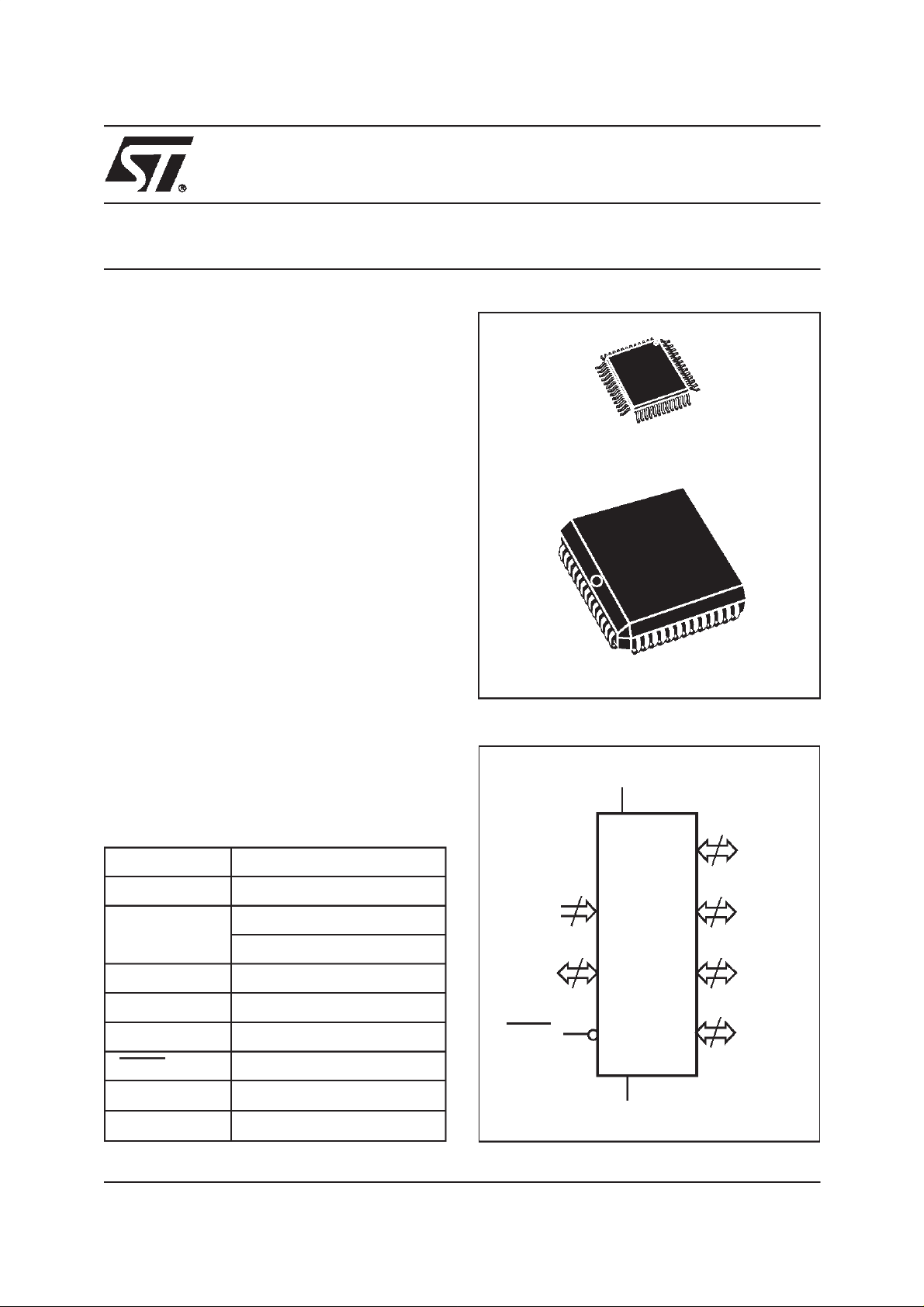
PQFP52 (T)
PLCC52 (K)
Figure 1. Logic Diagram
DESCRIPTION
The FLASH+PSD family of memory systems for
microcontrollers (MCUs) brings In-System-
Table 1. Signal Names
PA0-PA7 Port-A
PB0-PB7 Port-B
PC0-PC7
PD0-PD2 Port-D
AD0-AD15 Address/Data
CNTL0-CNTL2 Control
RESET Reset
V
CC
V
SS
June 2000
Complete data available on
Port-C
PC2 = Voltage Stand-by
Supply Voltage
Ground
Data-on-Disc CD-ROM
or at
www.st.com
V
CC
8
PA0-PA7
3
CNTL0-
CNTL2
AD0-AD15 PC0-PC7
RESET
16
FLASH+PSD
V
SS
8
PB0-PB7
8
3
PD0-PD2
AI02856
1/7
Page 2
M88 FAMILY
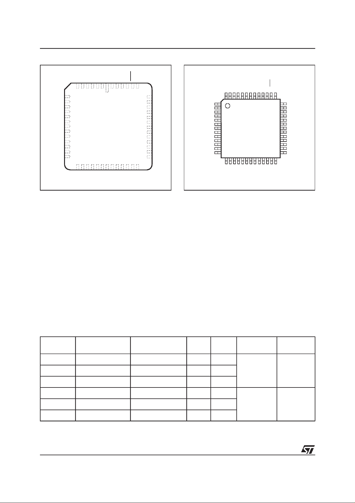
Figure 2A. PLCC Connections
RESET
PB7
CNTL1
CNTL2
CNTL0
47
48
49
50
51
AD15
46
AD14
45
AD13
44
AD12
43
AD11
42
AD10
41
AD9
40
AD8
39
VCC
38
AD7
37
AD6
36
AD5
35
AD4
34
PA0
AD1
AD2
AD3
AD0
AI02857
VCC
GND
PD2
PD1
PD0
PC7
PC6
PC5
PC4
PC3
PC2
PC1
PC0
PB0
PB1
PB2
PB3
PB4
PB5
GND
PB6
52
2
34567
PA4
PA3
GND
1
PA2
PA1
8
9
10
11
12
13
14
15
16
17
18
19
20
21222324252627282930313233
PA7
PA6
PA5
Programmability (ISP) to Flash memory and
programmable logic. The result is a simple and
flexible solution for embedded designs.
FLASH+PSD devices combine many of the
peripheral functions found in MCU based
applications. FLASH+PSD provides a glueless
interface to most commonly-used ROMless
MCUs.
Table 2 summarizes all the devices in the M88
Family.
The CPLD in the FLASH+PSD devices features
an optimized Macrocell logic architecture. The
Macrocell was created to address the unique
requirements of embedded system designs. It
allows direct connection between the system
address/data bus, and the internal FLASH+PSD
Figure 2B. PQFP Connections
PB0
PB1
PB2
PB3
PB4
PB5
GND
PB6
PB7
CNTL1
CNTL2
RESET
44
22
PA0
43
23
AD0
42
24
AD1
41
25
AD2
CNTLO
40
26
AD3
39
38
37
36
35
34
33
32
31 VCC
30
29
28
27 AD4
AD15
AD14
AD13
AD12
AD11
AD10
AD9
AD8
AD7
AD6
AD5
AI02858
PD2
PD1
PD0
PC7
PC6
PC5
PC4
VCC
GND
PC3
PC2
PC1
PC0
52
51
50
49
48
47
46
45
1
2
3
4
5
6
7
8
9
10
11
12
13
14
15
16
17
18
19
20
21
PA7
PA6
PA5
PA4
PA3
PA2
PA1
GND
registers, to simplify communication between the
MCU and other supporting devices.
The FLASH+PSD device includes a JTAG Serial
Programming interface, to allow In-System
Programming (ISP) of the entire device. This
feature reduces development time, simplifies the
manufacturing flow, and dramatically lowers the
cost of field upgrades. Using ST’s special FastJTAG programming, a design can be rapidly
programmed into the FLASH+PSD.
The innovative FLASH+PSD family solves key
problems faced by designers when managing
discrete Flash memory devices, such as:
– Complex address decoding
– In-System (first-time) Programming (ISP)
– Concurrent EEPROM or Flash memory
programming (IAP).
Table 2. Product Range
Part Number
Primary Flash
1
Memory
Secondary NVM
SRAM
2
I/O Ports Voltage Range Access Time
M8813F1Y 1 Mbit 256 Kbit EEPROM 16 Kbit 27
M8813F2Y 1 Mbit 256 Kbit Flash memory 16 Kbit 27
4.5-5.5 V
90 ns or
150 ns
M8834F2Y 2 Mbit 256 Kbit Flash memory 64 Kbit 27
M8813F1W 1 Mbit 256 Kbit EEPROM 16 Kbit 27
2.7-3.6 V 150 nsM8813F2W 1 Mbit 256 Kbit Flash memory 16 Kbit 27
M8834F2W 2 Mbit 256 Kbit Flash memory 64 Kbit 27
Note: 1. All products support: JTAG serial ISP, MCU parallel ISP, ISP Flash memory, ISP CPLD, Security features, Power Management
Unit (PMU), Automatic Power-down (APD)
2. SRAM may be backed up using an external battery.
2/7
Page 3
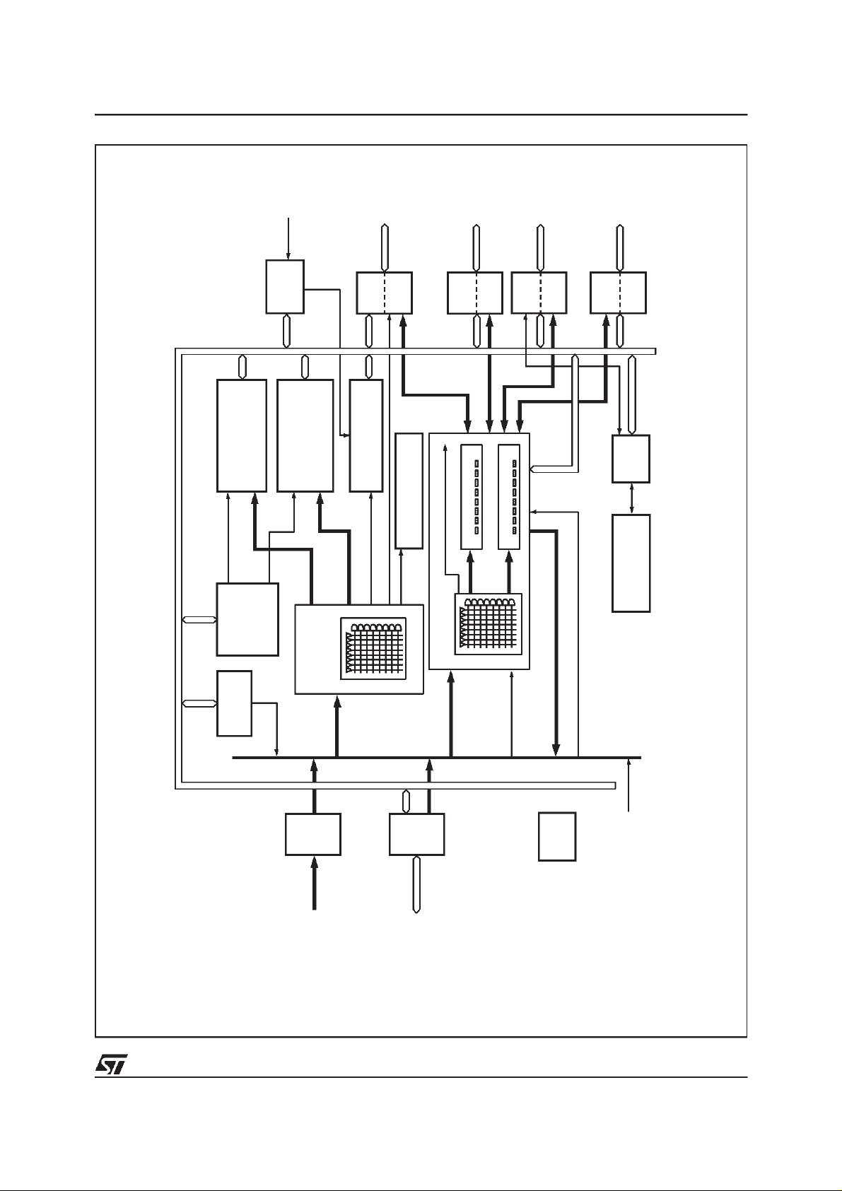
Figure 3. FLASH+PSD Block Diagram
)
PC2
(
VSTDBY
PA0 – PA7
PB0 – PB7
PC0 –PC7
M88 FAMILY
PD0 –PD2
ADDRESS/DATA/CONTROL BUS
FLASH MEMORY
1 OR 2 MBIT PRIMARY
EMBEDDED
PAGE
REGISTER
POWER
MANGMT
8 SECTORS
ALGORITHM
8
UNIT
4 SECTORS
(BOOT OR DATA)
256 KBITSECONDARY
EEPROM or FLASH MEMORY
SECTOR
SELECTS
)
DPLD
(
PLD
FLASH DECODE
SECTOR
SELECTS
73
PORT
PROG.
BACKUP SRAM
16 OR 64 KBIT BATTERY
SRAM SELECT
PERIP I/O MODE SELECTS
A
PORT
RUNTIME CONTROL
CSIOP
AND I/O REGISTERS
3 EXT CS TO PORT D
FLASH ISP CPLD
73
PORT
PROG.
PORT A ,B & C
16 OUTPUTMACROCELLS
(CPLD)
B
PORT
PORT A ,B & C
24 INPUT MACROCELLS
CLKIN
PORT
PROG.
C
PORT
MACROCELL FEEDBACK OR PORT INPUT
CLKIN
PORT
PORT
PROG.
JTAG
PLD, CONFIGURATION
D
SERIAL
CHANNEL
LOADER
& FLASHMEMORY
PLD
BUS
INPUT
CLKIN
PROG.
CNTL0,
CNTL1,
MCU BUS
CNTL2
INTRF.
ADIO
AD0 – AD15
PORT
GLOBAL
CONFIG. &
SECURITY
(PD1)
AI02861D
Sometimes computers try to be too clever for theirown good. Take this illustration for instance.
Just because somany of the labels are rotated through ninetydegrees, FrameMaker seems to
want to insist on telling the postscript file that I would find it more convenient to see this page
displayed inlandscape, rotated by ninety degrees. Well I wouldn’t. So I amputting inall this text
just to weight the average in this direction.
3/7
Page 4

M88 FAMILY
The JTAG Serial Interface block allows In-System
Programming (ISP). Embedded dual-bank
memories eliminates the need for anexternal Boot
EPROM or Flash memory, or an external
programmer. To simplify Flash memory updates,
program execution is performed from a secondary
Flash memory (for the M88xxF2x) or EEPROM
(for the M8813F1x) while the primary Flash
memory is being updated. This solution avoids the
complicated hardware and software overhead
necessary to implement IAP.
ST makes available a software development tool,
PSDsoft, that generates ANSI-C compliant code
for usewithyourtarget MCU. This code allowsyou
to manipulate the non-volatile memory (NVM)
within the FLASH+PSD. Code examples are also
provided for:
– Flash memory IAP via the UART of the host
MCU
– Memory paging to executecode across several
FLASH+PSD memory pages
– Loading, reading, and manipulation of
FLASH+PSD Macrocells by the MCU.
FLASH+PSD ARCHITECTURAL OVERVIEW
FLASH+PSD devices contain several major
functional blocks. Figure 3 shows the architecture
of the M88 FLASH+PSD device family. The
functions of each block are described briefly in the
following sections. Many of the blocks perform
multiple functions and are user configurable.
Memory
The 1 or 2 Mbit (128K x 8, or 256K x 8) Flash
memory is the primary memory of the
FLASH+PSD. It is divided into eight equally-sized
sectors that are individually selectable.
The 256 Kbit (32K x 8) secondary EEPROM or
Flash memory is divided into four equally-sized
sectors. Each sector is individually selectable.
The SRAM is intended for use as a scratch-pad
memory or as an extension to the MCU SRAM. If
an external battery is connected to Voltage Standby (VSTBY, PC2), data is retained in the event of
power failure.
Each sector of memory can be located in a
different address space as defined by the user.
The access times for all memory types includes
the address latching and DPLD decoding time.
The M8813F1x has 64 bytes of OTP memory for
product identifiers, serial numbers, calibration
constants, etc..
Page Register
The 8-bit Page Register expands the address
range of the MCU by up to 256 times. The paged
address can be used as part of the address space
to access external memory and peripherals, or
internal memory and I/O. The Page Register can
also be used to change the address mapping of
sectors of the Flash memories into different
memory spaces for IAP.
PLDs
The device contains two PLDs, the Decode PLD
(DPLD) and the Complex PLD (CPLD), each
optimized for a different function, as shown in
Table 3. The functional partitioning of the PLDs
reduces power consumption, optimizes cost/
performance, and eases design entry.
The DPLD is used to decode addresses and to
generate Sector Select signals for the
FLASH+PSD internal memory and registers. The
DPLD has 17 combinatorial outputs, which are
used to select memory sectors and JTAG. The
CPLD has 16 Output Macrocells (OMC) and 3
combinatorial outputs. The CPLD also has 24
Input Macrocells (IMC) that can be configured as
inputs to the PLDs. The PLDs receive their inputs
from the PLD Input Bus and are differentiated by
their output destinations, number ofproduct terms,
and Macrocells.
The PLDs consume minimal power. The speed
and power consumption of the PLD is controlled
by the Turbo bit in the PMMR0 register and other
bits in the PMMR2 registers. These registers are
set by the MCU at run-time. There is a slight
penalty to PLD propagation time when invoking
the power management features.
I/O Ports
The FLASH+PSD has 27 individually configurable
I/O pins distributed over the four ports (Port A, B,
C, and D). Each I/O pin can be individually
configured for different functions. Ports can be
configured as standard MCU I/O ports, PLD I/O, or
latched address outputs for MCUs using
multiplexed address/data buses. Ports A and B
can be configured to be open drain.
The JTAG pins can be enabled on Port C for InSystem Programming (ISP).
Ports A and B can also be configured as a data
port for a non-multiplexed bus or multiplexed
address/data bus for certain types of 8-bit MCUs.
MCU Bus Interface
FLASH+PSD interfaces easily with most 8-bit
MCUs that have either multiplexed or nonmultiplexed address/data buses. The device is
configured to respond to the MCU’s control
signals, which are also used asinputsto the PLDs.
Where there is a requirement to use a 16-bit data
bus to interface to a 16-bit MCU, two PSDs must
be used. For examples, please see the full data
sheet.
4/7
Page 5

M88 FAMILY
Table 3. PLD I/O
Name Inputs Outputs
Decode PLD (DPLD) 73 17 42
Complex PLD (CPLD) 73 19 140
Product
Terms
JTAG Port
In-System Programming (ISP) can be performed
through the JTAG signals on Port C. This serial
interface allows complete programming of the
entire FLASH+PSD device. A blank devicecan be
completely programmed for the first time after it is
soldered to the board. The JTAG signals (TMS,
TCK, TSTAT, TERR, TDI, TDO) can be
multiplexed with other functionson Port C. Table 4
indicates the JTAG pin assignments. Four-pin
JTAG is also fully supported.
In-System Programming (ISP)
Using the JTAG signals on Port C, the entire
FLASH+PSD device can be programmed or
erased without the use of the MCU. The primary
Flash memory can also be programmed in-system
by the MCU executing the programming
algorithms out of the secondary memory, or
SRAM. The secondary memory can be
programmed thesameway by executing out of the
primary Flash memory. The PLD or other
FLASH+PSD Configuration blocks can be
programmed through the JTAG port or a device
insertion programmer. Table 5 indicates which
programming methods can program different
functional blocks of the FLASH+PSD.
Power Management Unit (PMU)
The Power Management Unit (PMU) gives the
user controlof the power consumption on selected
functional blocks based on system requirements.
The PMU includes an Automatic Power-down
(APD) Unit that turns off device functions during
MCU inactivity. The APD Unit has a Power-down
mode that helps reduce power consumption.
The FLASH+PSD also has some bits that are
configured at run-time by the MCU to reduce
Table 4. JTAG SIgnals on Port C
Port C Pins JTAG Signal
PC0 TMS
PC1 TCK
PC3 TSTAT
PC4 TERR
PC5 TDI
PC6 TDO
power consumption of the CPLD. The Turbo bit in
the PMMR0 register can be reset to 0 and the
CPLD latches its outputs and goes to sleep until
the next transition on its inputs.
Additionally, bits in the PMMR2 register can be set
by the MCU to block signals from entering the
CPLD to reduce power consumption. Please see
the full data sheet for more details.
SECURITY AND NVM SECTOR PROTECTION
A security bit in the Protection Register enables
the software project, coded in the FLASH+PSD, to
be locked up. This bit is only accessible by the
system designer from the JTAG serial port, or from
a parallel insertion programmer. It cannot be
accessed from the MCU. The only way a security
bit can be cleared is to erase the entire chip.
The contents of the sectors of the primary and
secondary NVM blocks can beprotectedusingbits
in the Protection Registers. These bits are
accessible from the MCU in the application code,
or from a programmer during the set-up
procedure.
Table 5. Methods of Programming Different Functional Blocks of the FLASH+PSD
Functional Block JTAG Programming Device Programmer IAP
Primary Flash Memory Yes Yes Yes
Secondary EEPROM or Flash memory Yes Yes Yes
PLD Array (DPLD and CPLD) Yes Yes No
FLASH+PSD Configuration Yes Yes No
OTP Row No Yes Yes
5/7
Page 6

M88 FAMILY
Table 6. Ordering Information Scheme
Example: M88 1 3 F 1 W – 15 T 1 T
SRAM Capacity Option
1 16 Kbit T Tape& Reel Packing
3 64 Kbit
Temperature Range
Flash Memory Capacity 10to70°C (commercial)
3 1 Mbit (128K x 8) 6 –40 to 85 °C (industrial)
4 2 Mbit (256K x 8)
2nd Non Volatile Memory Package
1 256 Kbit EEPROM K PLCC52
2 256 Kbit Flash memory T PQFP52
Operating Voltage Speed
4.5 V to 5.5 V
Y
W 2.7 V to 3.6 V -15 150 ns
Note: 1. Available on the 4.5 to 5.5V range, only.
-90
90 ns
ORDERING INFORMATION SCHEME
When delivered from ST, the FLASH+PSD device
has all bits in the memory and PLDs set to 1. The
FLASH+PSD Configuration Registerbits are setto
0. The code, configuration, and PLD logic are
loaded using the programming procedure.
Information for programming the device is
available directly from ST. Please contact your
local sales representative.
The notation used for the device number is as
shown in Table 6. For a list of available options
(speed, package, etc.) or for further information on
any aspect of this device, please see the full data
sheet (please consult our pages on the world wide
web:
www.st.com/flashpsd
). Alternatively, please
contact your nearest ST Sales Office.
1
6/7
Page 7

M88 FAMILY
Information furnished is believed to be accurate and reliable. However, STMicroelectronics assumes no responsibility for the consequences
of useof such information norfor any infringement ofpatents or other rights of thirdparties which may result from its use.No license is granted
by implication or otherwise under any patent or patent rights of STMicroelectronics. Specifications mentioned in this publication are subject
to change without notice. This publication supersedes and replaces all information previously supplied. STMicroelectronics products are not
authorized for use ascritical components in life support devices or systems without express writtenapproval of STMicroelectronics.
2000 STMicroelectronics - All Rights Reserved
The ST logo is a registered trademark of STMicroelectronics.
All other names are the property of their respective owners.
STMicroelectronics GROUP OF COMPANIES
Australia - Brazil - China - Finland - France - Germany - Hong Kong - India - Italy - Japan -Malaysia - Malta - Morocco - Singapore - Spain -
Sweden - Switzerland - United Kingdom - U.S.A.
http://www.st.com
7/7
 Loading...