

Datasheet M74HCU04TTR, M74HCU04RM13TR, M74HCU04M1R, M74HCU04B1R Datasheet (SGS Thomson Microelectronics)
Page 1
M74HCU04
HEX INVERTER (SINGLE STATE)
■ HIGH SPEED:
t
= 5ns (TYP.) at VCC = 6V
PD
■ LOW POWER DISSIPATION:
I
= 1µA(MAX.) at TA=25°C
CC
■ HIGH NOISE IMMUNITY:
V
= V
NIH
■ SYMMETRICAL OUTPUT IMPEDANCE:
|I
| = IOL = 4mA (MIN)
OH
■ BALANCED PROPAGATION DELAYS:
t
≅ t
PLH
■ WIDE OPERATING VOLTAGE RANGE:
V
(OPR) = 2V to 6V
CC
■ PIN AND FUNCTION COMPATIBLE WITH
= 10% VCC (MIN.)
NIL
PHL
74 SERIES 04
DESCRIPTION
The M74HCU04 is an high speed CMOS HEX
INVERTER (SINGLE STATE) fabricated with
silicon gate C
2
MOS technology.
As internal circuit is comp osed of a single stage
inverter, it can be used in crystal oscillator.
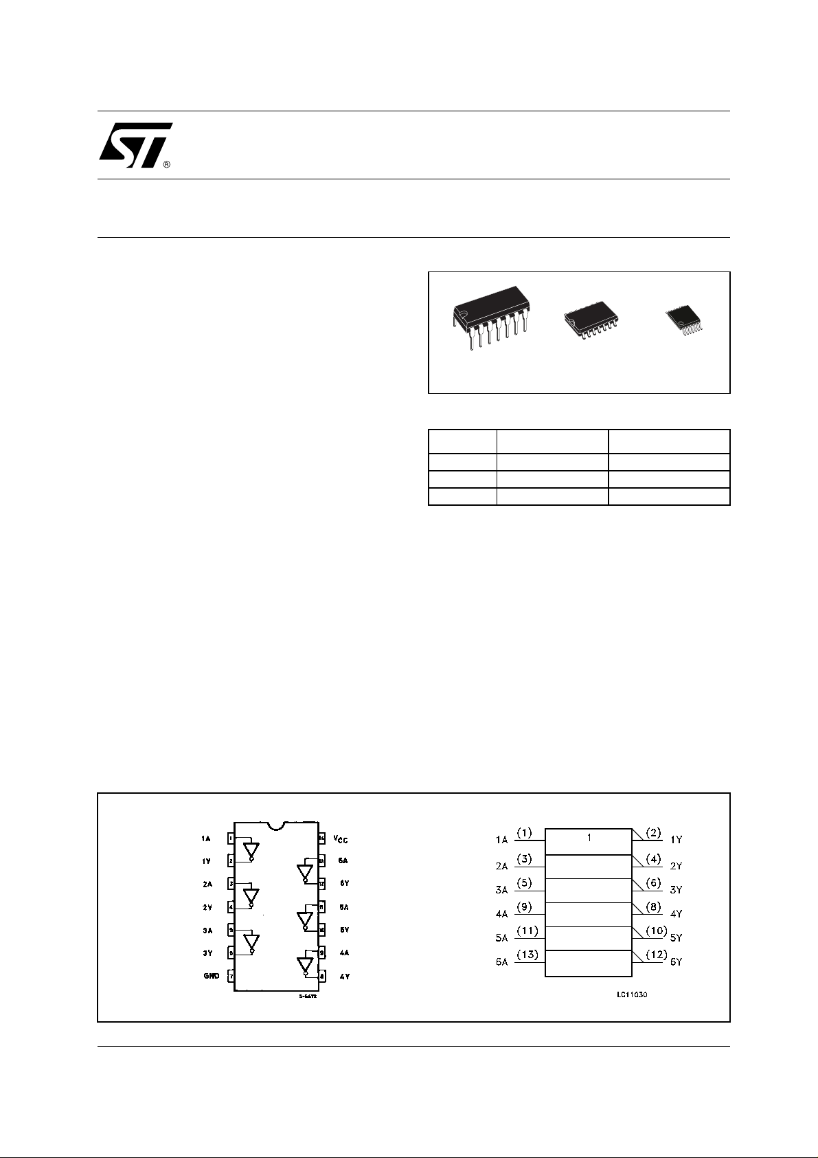
TSSOPDIP SOP
ORDER CODES
PACKAGE TUBE T & R
DIP M74HCU04B1R
SOP M74HCU04M1R M74HCU04RM13TR
TSSOP M74HCU04TTR
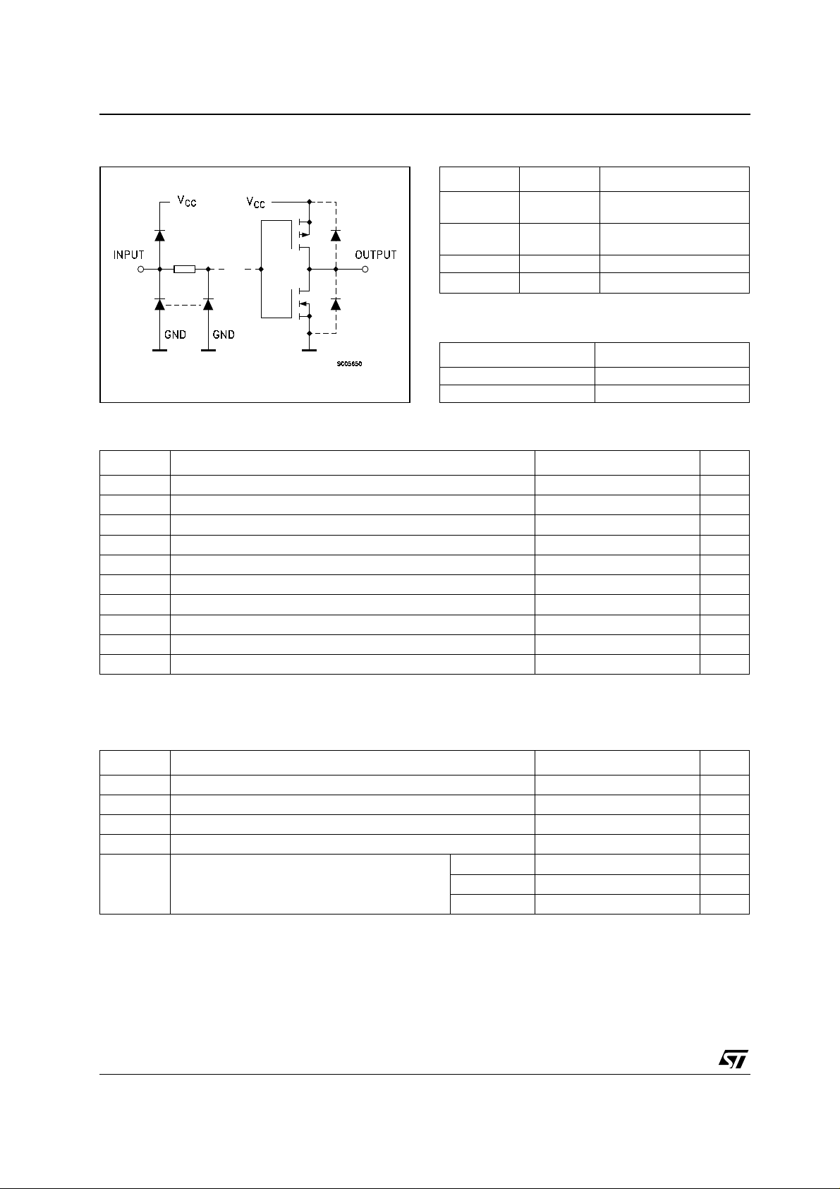
All inputs are equipped with protection circuits
against static discharge and transient excess
voltage.
PIN CONNECTION AND IEC LOGIC SYMBOLS
1/8April 2002
Page 2
M74HCU04
INPUT AND OUTPUT EQUIVALENT CIRCUIT PIN DESCRIPTION
PIN No SYMBOL NAME AND FUNCTION
1, 3, 5, 9, 1 1,
13
2, 4, 6, 8, 10,
12
7 GND Ground (0V)
14
TRUTH TABLE
ABSOLUTE MAXIMUM RATINGS
Symbol Parameter Value Unit
V
V
V
I
I
OK
I
or I
I
CC
P
T
T
Absolute Maximum Ratings are those values beyond which damage to the device may occur. Functional operation under these conditions is
not implied
(*) 500mW at 65
Supply Voltage
CC
DC Input Voltage -0.5 to VCC + 0.5
I
DC Output Voltage -0.5 to VCC + 0.5
O
DC Input Diode Current
IK
DC Output Diode Current
DC Output Current
O
DC VCC or Ground Current
GND
Power Dissipation
D
Storage Temperature
stg
Lead Temperature (10 sec)
L
°C; derate to 300mW by 10mW/°C from 65°C to 85°C
1A to 6A Data Inputs
1Y to 6Y Data Outputs
V
CC
Positive Supply Voltage
AY
LH
HL
-0.5 to +7 V
V
V
20 mA
±
20 mA
±
25 mA
±
50 mA
±
500(*) mW
-65 to +150 °C
300 °C
RECOMMENDED OPERATING CONDITIONS
Symbol Parameter Value Unit
2/8
V
V
V
T
t
r
Supply Voltage
CC
Input Voltage 0 to V
I
Output Voltage 0 to V
O
Operating Temperature
op
Input Rise and Fall Time VCC = 2.0V
, t
f
V
V
CC
CC
= 4.5V
= 6.0V
2 to 6 V
CC
CC
-55 to 125 °C
0 to 1000 ns
0 to 500 ns
0 to 400 ns
V
V
Page 3
DC SPECIFICATIONS
Symbol Parameter
V
V
V
V
I
High Level Input
IH
Voltage
Low Level Input
IL
Voltage
High Level Output
OH
Voltage
Low Level Output
OL
Voltage
I
Input Leakage
I
Current
Quiescent Supply
CC
Current
M74HCU04
Test Condition Value
T
= 25°C
V
CC
(V)
A
Min. Typ. Max. Min. Max. Min. Max.
2.0 1.7 1.7 1.7
6.0 4.8 4.8 4.8
2.0 0.3 0.3 0.3
6.0 1.2 1.2 1.2
2.0
4.5
6.0
4.5
6.0
2.0
4.5
6.0
4.5
6.0
6.0
6.0
IO=-20 µA
I
=-20 µA
O
I
=-20 µA
O
I
=-4.0 mA
O
I
=-5.2 mA
O
IO=20 µA
I
=20 µA
O
I
=20 µA
O
I
=4.0 mA
O
I
=5.2 mA
O
= VCC or GND
V
I
= VCC or GND
V
I
1.8 2.0 1.8 1.8
4.0 4.5 4.0 4.0
5.5 5.9 5.5 5.5
4.18 4.31 4.13 4.10
5.68 5.8 5.63 5.60
0.0 0.2 0.2 0.2
0.0 0.5 0.5 0.5
0.1 0.5 0.5 0.5
0.17 0.26 0.33 0.40
0.18 0.26 0.33 0.40
-40 to 85°C -55 to 125°C
±
0.1
1
±
±
11020
Unit
1
V4.5 3.6 3.6 3.6
V4.5 0.9 0.9 0.9
V
V
A
µ
A
µ
AC ELECTRICAL CHARACTERISTICS (C
= 50 pF, Input tr = tf = 6ns)
L
Test Condition Value
T
Symbol Parameter
t
TLH tTHL
Output Transition
Time
V
CC
(V)
2.0 30 75 95 110
= 25°C
A
-40 to 85°C -55 to 125°C
Min. Typ. Max. Min. Max. Min. Max.
Unit
ns4.5 8151922
6.0 7131619
t
PLH tPHL
Propagation Delay
Time
2.0 18 60 75 90
ns4.5 6121518
6.0 5101315
CAPACITIVE CHARACTERISTICS
Test Condition Value
T
Symbol Parameter
V
CC
(V)
C
C
1) CPD is defined as the value of the IC’s internal equivalent capacitance which is calculated from the operating current consumption without
load. (R ef er to Test Circ ui t). Averag e operating current can be obtained by t he following equation. I
Input Capacitance
IN
Power Dissipation
PD
Capacitance (note 1)5.0 13 pF
5.0 5101010pF
= 25°C
A
Min. Typ. Max. Min. Max. Min. Max.
-40 to 85°C -55 to 125°C
= CPD x VCC x fIN + ICC
CC(opr)
Unit
3/8
Page 4

M74HCU04
TEST CIRCUIT
CL = 50pF or equivalent (in cludes jig and probe capaci tance)
R
= Z
of pulse generator (typically 50Ω)
T
OUT
WAVEFORM : PROPAGATION DELAY TIME (f=1MHz; 50% duty cycle)
4/8
Page 5

M74HCU04
Plastic DIP-14 MECHANICAL DATA
mm. inch
DIM.
MIN. TYP MAX. MIN. TYP. MAX.
a1 0.51 0.020
B 1.39 1.65 0.055 0.065
b 0.5 0.020
b1 0.25 0.010
D 20 0.787
E 8.5 0.335
e 2.54 0.100
e3 15.24 0.600
F 7.1 0.280
I 5.1 0.201
L 3.3 0.130
Z 1.27 2.54 0.050 0.100
P001A
5/8
Page 6

M74HCU04
SO-14 MECHANICAL DATA
DIM.
A 1.75 0.068
a1 0.1 0.2 0.003 0.007
a2 1.65 0.064
b 0.35 0.46 0.013 0.018
b1 0.19 0.25 0.007 0.010
C 0.5 0.019
c1 45° (typ.)
D 8.55 8.75 0.336 0.344
E 5.8 6.2 0.228 0.244
e 1.27 0.050
e3 7.62 0.300
F 3.8 4.0 0.149 0.157
G 4.6 5.3 0.181 0.208
L 0.5 1.27 0.019 0.050
M 0.68 0.026
S8° (max.)
MIN. TYP MAX. MIN. TYP. MAX.
mm. inch
6/8
PO13G
Page 7

M74HCU04
TSSOP14 MECHANICAL DATA
mm. inch
DIM.
MIN. TYP MAX. MIN. TYP. MAX.
A 1.2 0.047
A1 0.05 0.15 0.002 0.004 0.006
A2 0.8 1 1.05 0.031 0.039 0.041
b 0.19 0.30 0.007 0.012
c 0.09 0.20 0.004 0.0089
D 4.9 5 5.1 0.193 0.197 0.201
E 6.2 6.4 6.6 0.244 0.252 0.260
E1 4.3 4.4 4.48 0.169 0.173 0.176
e 0.65 BSC 0.0256 BSC
K0° 8°0° 8°
L 0.45 0.60 0.75 0.018 0.024 0.030
A2
A
A1
b
e
c
K
L
E
D
E1
PIN 1 IDENTIFICATION
1
0080337D
7/8
Page 8

M74HCU04
Information furnished is believed to be accurate and reliable. However, STMicroelectronics assumes no responsibility f or the
consequences of use of such informatio n nor for any infringement of paten ts or o ther rig hts of t hird part ies which ma y result from
its use. No license is granted by implication or otherwise under any patent or patent rights of STMicroelectronics. Specifications
mentioned in this publication are subject to change without notice. This publication supersedes and replaces all information
previousl y suppl ied. STM icroel ectronics produc ts are not auth orized for use as c ritica l compone nts in l ife s upport dev ices or
systems without express written approval of STMicroelectronics.
Australia - Brazil - Canada - China - Finland - France - Germany - Hong Kong - India - Israel - Italy - Japan - Malaysia - Malta - Morocco
© The ST logo is a registered trademark of STMicroelectronics
© 2002 STMicroelectronics - Prin ted in Italy - All Rights Reserved
STMicroelectronics GROUP OF COMPANIES
Singapore - Spain - Sweden - Switzerland - United Kingdom - United States.
© http://www.st.com
8/8
 Loading...