

Page 1
.HIGH SPEED
tPD= 15 ns(TYP.) AT VCC=5V
.LOWPOWER DISSIPATION
ICC=2 µA (MAX.) AT TA=25°C
.COMPATIBLE WITHTTL OUTPUTS
VIH= 2 V (MIN.) VIL= 0.8 V (MAX.)
.OUTPUT DRIVE CAPABILITY 10 LSTTL LOADS
.SYMMETRICALOUTPUT IMPEDANCE
IOH =IOL= 4 mA (MIN.)
.PIN AND FUNCTION COMPATIBLE WITH
54/74LS75
4 BIT D TYPE LATCH
B1R
(PlasticPackage)
M54HCT75
M74HCT75
F1R
(CeramicPackage)
DESCRIPTION
TheM54/74HCT7 5isahighspeedCMOS4-BITD-TYP E
LATCH fabricatedin silicongate C2MOStechnology. It
has the same high speed performa nce of LSTTL combined withtrueCMOS lowpower consumption. It contains
two groups of 2-bi t latches control led by an enable input
(G1 • 2orG3•4). These two latch groups can be used
indifferentcir cuits.Each latch has Qand Q outputs (1Q 4Qand1Q - 4Q).The dataapplied to thedata input is
transfere d to theQ and Q outputswhen theenable input
is taken high and the outputs will follow the data input as
long as the enab le input is kept high. When the enabl e
input is taken low,the information data applied to the data
input isretained at the outputs. Allinputs areequipped with
protection circuits against static discharge and transi ent
excessvoltage .Thisintegr atedcircu ithasinp utandoutput
characteris ticsthat arefullycompatiblewith54/74LSTTL
logic families. M54/74HCT devices are designed to directlyinterfac eHSC2MOSsystemswithTTLandNMOS
componen ts. They are also plug in replaceme n ts for
LSTTLdevices givinga reductionof powercons umptio n.
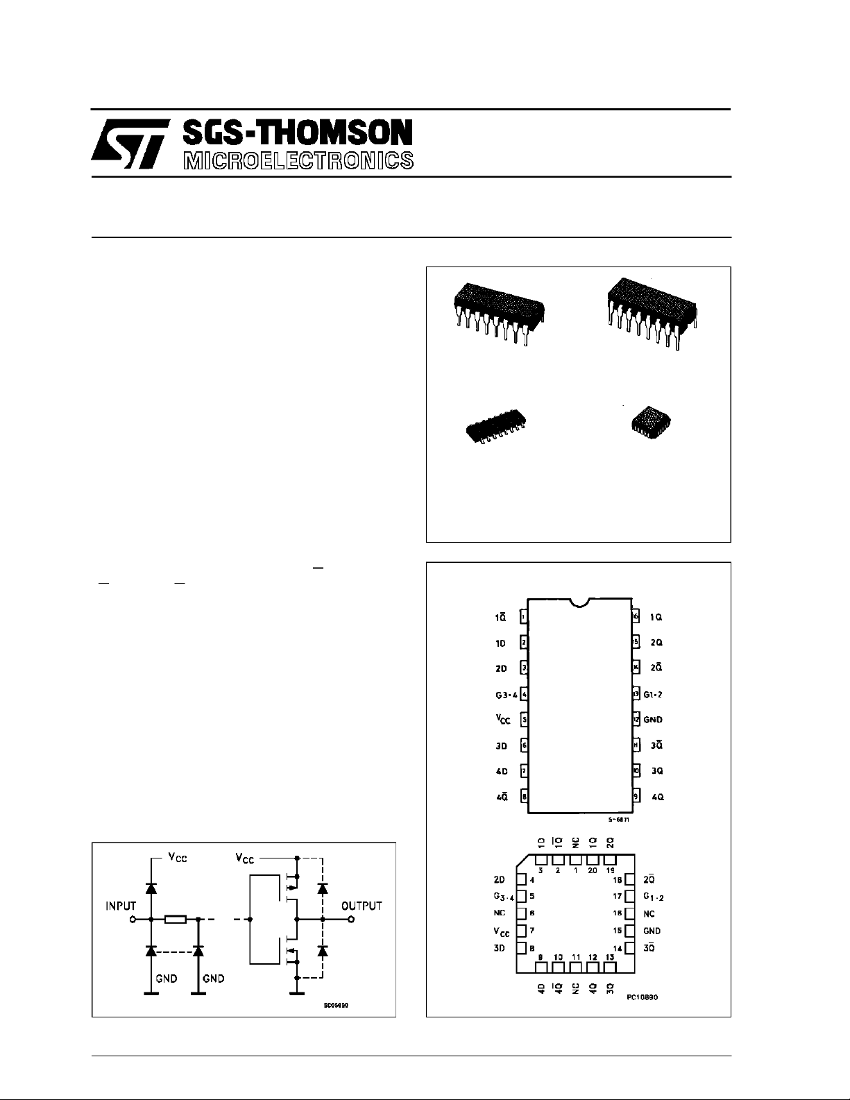
INPUT AND OUTPUT EQUIVALENT CIRCUIT
M1R
(MicroPackage)
ORDER CODES :
M54HC T75F1R M74H CT75M1R
M74HC T75B1R M74HCT75C1R
PIN CONNECTIONS(top view)
C1R
(Chip Carrier)
January 1993
NC =
No Internal
Connection
1/9
Page 2
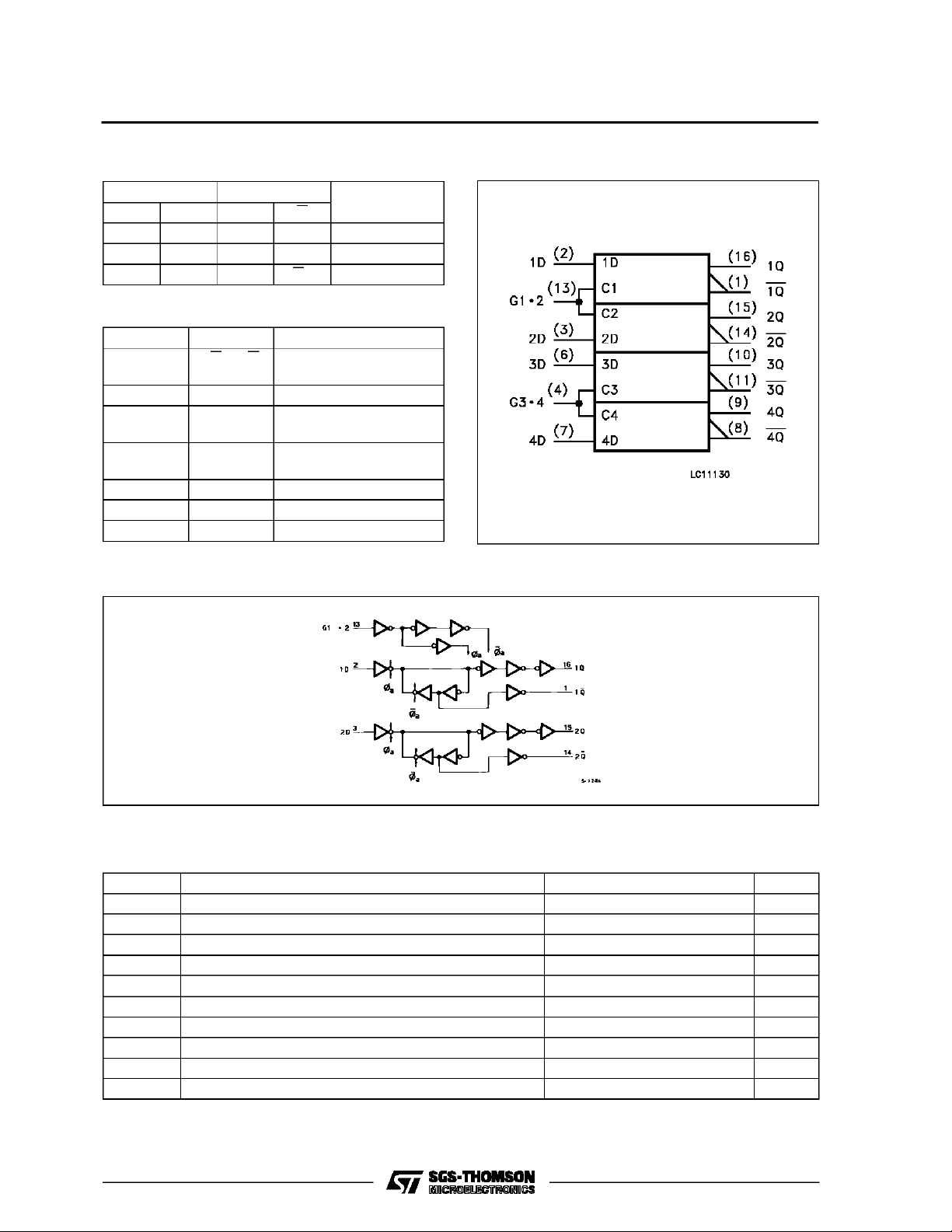
M54/M74HCT75
TRUTH TABLE
INPUTS OUTPUTS
DGQQ
LHLH
HHHL
X L Qn Qn LATCH
FUNCTION
PIN DESCRIPTION
PIN No SYMBOL NAME AND FUNCTION
1, 4, 11, 8 1Q to 4Q Complementary Latch
Outputs
2, 3, 6, 7 1D to 4D Data Inputs
4G3•4 Latch Enable Input,
latches 3 and 4
13 G1 • 2 Latch Enable Input,
latches 1 and 2
15, 15, 10, 9 1Q to 4Q Latch Outputs
12 GND Ground (0V)
5V
CC
Positive Supply Voltage
SCHEM ATIC C I R CUI T
IEC LOGIC SYMBOL
ABSOLU TE MAXIMU M RAT INGS
Symbol Parameter Value Unit
V
CC
V
V
O
I
IK
I
OK
I
O
or I
I
CC
P
D
T
stg
T
L
AbsoluteMaximumRatingsarethosevaluesbeyondwhichdamage tothedevicemayoccur. Functionaloperationunder theseconditionisnotimplied.
(*)500 mW: ≅ 65oC derateto300 mWby 10mW/oC: 65oCto85oC
2/9
Supply Voltage -0.5 to +7 V
DC Input Voltage -0.5 to VCC+ 0.5 V
I
DC Output Voltage -0.5 to VCC+ 0.5 V
DC Input Diode Current ± 20 mA
DC Output Diode Current ± 20 mA
DC Output Source Sink Current Per Output Pin ± 25 mA
DC VCCor Ground Current ± 50 mA
GND
Power Dissipation 500 (*) mW
Storage Temperature -65 to +150
Lead Temperature (10 sec) 300
o
C
o
C
Page 3
M54/M74HCT75
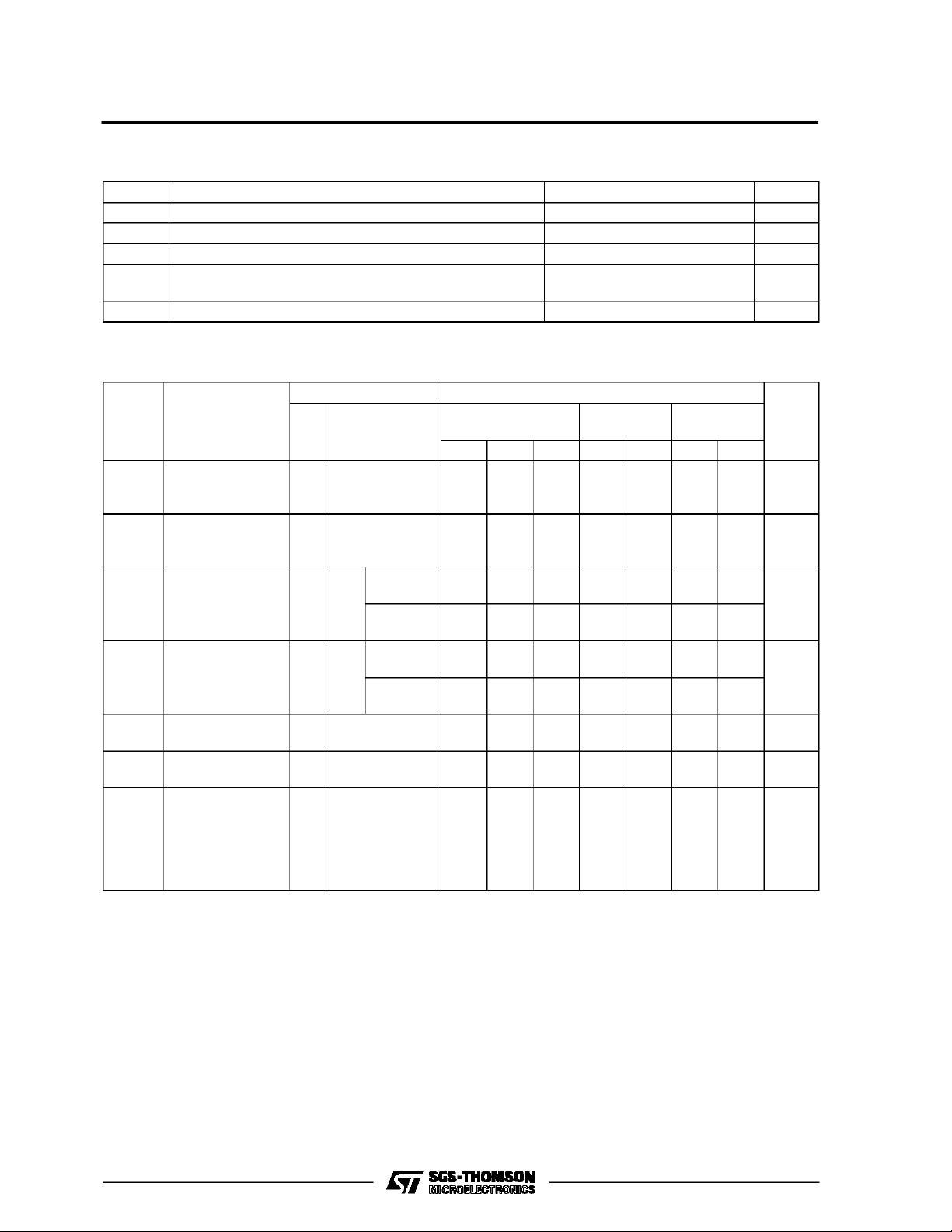
RECO MM ENDED OPERATI N G C ONDI TIONS
Symbol Parameter Value Unit
V
V
V
T
t
r,tf
DC SPECIF ICATIO NS
Symbol Parameter
V
V
V
OH
V
OL
I
I
CC
∆I
Supply Voltage 4.5 to 5.5 V
CC
Input Voltage 0 to V
I
Output Voltage 0 to V
O
Operating Temperature: M54HC Series
op
M74HC Series
CC
CC
-55 to +125
-40 to +85
Input Rise and Fall Time (VCC= 4.5 to 5.5V) 0 to 500 ns
Test Conditions Value
T
High Level Input
IH
Voltage
V
(V)
4.5
=25oC
CC
A
54HC and 74HC
Min. Typ. Max. Min. Max. Min. Max.
2.0 2.0 2.0 V
to
-40 to 85oC
74HC
-55 to 125oC
5.5
Low Level Input
IL
Voltage
4.5
to
0.8 0.8 0.8 V
5.5
High Level
Output Voltage
Low Level Output
Voltage
Input Leakage
I
Current
Quiescent Supply
VI=
IO=-20 µA 4.4 4.5 4.4 4.4
V
IH
4.5
or
I
=-4.0 mA 4.18 4.31 4.13 4.10
O
V
IL
VI=
IO=20µA 0.0 0.1 0.1 0.1
V
IH
4.5
or
I
= 4.0 mA 0.17 0.26 0.33 0.4
O
V
IL
VI=VCCor GND ±0.1 ±1 ±1 µA
5.5
5.5 VI=VCCor GND 2 20 40 µA
Current
Additional worst
CC
case supply
current
5.5 Per Input pin
V
= 0.5V or
I
VI= 2.4V
2.0 2.9 3.0 mA
Other Inputs at
VCCor GND
IO=0
54HC
V
V
o
C
o
C
Unit
V
V
3/9
Page 4

M54/M74HCT75
AC ELECTRICAL CHARACTERISTICS (CL=50pF,Inputtr=tf=6ns)
Test Conditions Value
T
=25oC
Symbol Parameter
t
t
t
t
TLH
THL
PLH
PHL
Output Transition
Time
Propagation
Delay Time
V
CC
(V)
4.5 8151922
4.5 18 28 35 42
A
54HC and 74HC
Min. Typ. Max. Min. Max. Min. Max.
(DATA-Q)
t
t
PLH
PHL
Propagation
Delay Time
4.5 21 33 41 50
(G-Q)
t
W(H)
Minimum Pulse
4.5 8151922
Width (G)
t
Minimum Set-up
s
4.5 4101315
Time
t
h
Minimum Hold
4.5 5 5 8
Time
C
C
PD
Input Capacitance 5 10 10 10 pF
IN
(*) Power Dissipation
61
Capacitance
(*) CPDisdefined as the valueof the IC’s internal equivalent capacitance which is calculatedfromthe operatingcurrent consumption without load.
(Referto Test Circuit).Average operting current can be obtained bythefollowingequation. ICC(opr) = CPD•VCC•fIN+I
-40 to 85oC
74HC
-55 to 125oC
54HC
CC
Unit
ns
ns
ns
ns
ns
ns
pF
SWITCHING CHARACTERISTICS TEST
WAVEFORM
TEST CIRCUIT ICC(Opr)
* INPUT WAVEFORM IS THE SAME AS THAT IN CASE OF
SWITCHINGCHARACTERISTICSTEST.
4/9
Page 5

Plastic DIP16 (0.25) MECHANICAL DATA
M54/M74HCT75
DIM.
MIN. TYP. MAX. MIN. TYP. MAX.
a1 0.51 0.020
B 0.77 1.65 0.030 0.065
b 0.5 0.020
b1 0.25 0.010
D 20 0.787
E 8.5 0.335
e 2.54 0.100
e3 17.78 0.700
F 7.1 0.280
I 5.1 0.201
L 3.3 0.130
Z 1.27 0.050
mm inch
P001C
5/9
Page 6

M54/M74HCT75
Ceramic DIP16/1 MECHANICAL DATA
DIM.
MIN. TYP. MAX. MIN. TYP. MAX.
A 20 0.787
B 7 0.276
D 3.3 0.130
E 0.38 0.015
e3 17.78 0.700
F 2.29 2.79 0.090 0.110
G 0.4 0.55 0.016 0.022
H 1.17 1.52 0.046 0.060
L 0.22 0.31 0.009 0.012
M 0.51 1.27 0.020 0.050
N 10.3 0.406
P 7.8 8.05 0.307 0.317
Q 5.08 0.200
mm inch
6/9
P053D
Page 7

SO16 (Narrow) MECHANICAL DATA
M54/M74HCT75
DIM.
MIN. TYP. MAX. MIN. TYP. MAX.
A 1.75 0.068
a1 0.1 0.2 0.004 0.007
a2 1.65 0.064
b 0.35 0.46 0.013 0.018
b1 0.19 0.25 0.007 0.010
C 0.5 0.019
c1 45° (typ.)
D 9.8 10 0.385 0.393
E 5.8 6.2 0.228 0.244
e 1.27 0.050
e3 8.89 0.350
F 3.8 4.0 0.149 0.157
G 4.6 5.3 0.181 0.208
L 0.5 1.27 0.019 0.050
M 0.62 0.024
S8°(max.)
mm inch
P013H
7/9
Page 8

M54/M74HCT75
PLCC20 MECHANICAL DATA
DIM.
MIN. TYP. MAX. MIN. TYP. MAX.
A 9.78 10.03 0.385 0.395
B 8.89 9.04 0.350 0.356
D 4.2 4.57 0.165 0.180
d1 2.54 0.100
d2 0.56 0.022
E 7.37 8.38 0.290 0.330
e 1.27 0.050
e3 5.08 0.200
F 0.38 0.015
G 0.101 0.004
M 1.27 0.050
M1 1.14 0.045
mm inch
8/9
P027A
Page 9

M54/M74HCT75
Information furnished is believed to be accurate and reliable. However, SGS-THOMSON Microelectronics assumes no responsability for the
consequences of use of such information nor for any infringement of patents or other rights of third parties which may results from its use. No
license is granted byimplication or otherwise under any patent or patentrights of SGS-THOMSON Microelectronics. Specificationsmentioned
in this publication are subject to change without notice. This publication supersedes and replaces all information previously supplied.
SGS-THOMSON Microelectronicsproducts are not authorized foruse ascritical componentsin life support devices or systems without express
written approval of SGS-THOMSON Microelectonics.
1994 SGS-THOMSON Microelectronics - All Rights Reserved
Australia - Brazil - France - Germany - Hong Kong - Italy - Japan - Korea - Malaysia - Malta - Morocco - The Netherlands -
Singapore -Spain - Sweden- Switzerland -Taiwan - Thailand - United Kingdom - U.S.A
SGS-THOMSON Microelectronics GROUP OF COMPANIES
9/9
 Loading...