

Page 1
8BIT ADDRESSABLE LATCH/DECODER/RELAIS
DRIVER (OPEN DRAIN,INVERTING OUTPUT)
■ LOW POW ERDISSIPATION
I
=4 µA (MAX.)AT TA=25°C
CC
■ COMPATIBLEWITHTTLOUTPUTS
=2V(MIN)VIL=0.8V(MAX)AT5V
V
IH
■ OUTPUTDRIVECAPABILITY
90LSTTLLOADS
■ HIGHCURRENTOPENDRAINOUTPUTUP
TO80 mA
The M74HCT7259 is a high speed CMOS 8 BIT
ADDRESSABLELATCH/DECODER fabricated in
silicon gate C2MOS technology. It has the same
high speed performanceof LSTTLcombined with
trueCMOS low powerconsumption.
The M74HCT7259 has single data input (D) 8
LATCH inverted OUTPUTS (Q0-Q7), 3 address
inputs (A, B and C), common enable input
(ENABLE) and a common CLEAR input. To
operatethis device as an addressablelatch, data
is held on the D input, and the address of the
latch into which the data is to be entered is held
on the A,B and C inputs.
When ENABLE is taken low the data flows
through to the address output. The data is stored
on the positive-going edge of the ENABLE pulse.
All unadressed latches will remain unaffected.
With ENABLE in the high state the device is
deselected and all latches remain in their
previous state, unaffected by changes on the
M74HCT7259
PRELIMINARY DATA
SOPDIP
ORDER CODES
PACK AG E TUBE T & R
DIP M74HCT7259B1R
SOP M74HCT7259M1R M74HCT7259M1RTR
data or address inputs. To eliminate the
possibility of entering erroneous data into the
latches, the ENABLE should be held high
(inactive) while the address lines are changing. If
ENABLE is held high and CLEAR is taken low all
eight latches are cleared to the HIGH (OFF)
state. If ENABLE is low all latches except the
addressed latch will be cleared. The address
latch will instead be the complement of the D
input,effectively implementing a 3 to 8 line
decoder. Internal clamp diodes protect the open
drain outputs against over voltages due to
inductiveloads.
All inputs are equipped with protection circuits
against static discharge and transient excess
voltage.
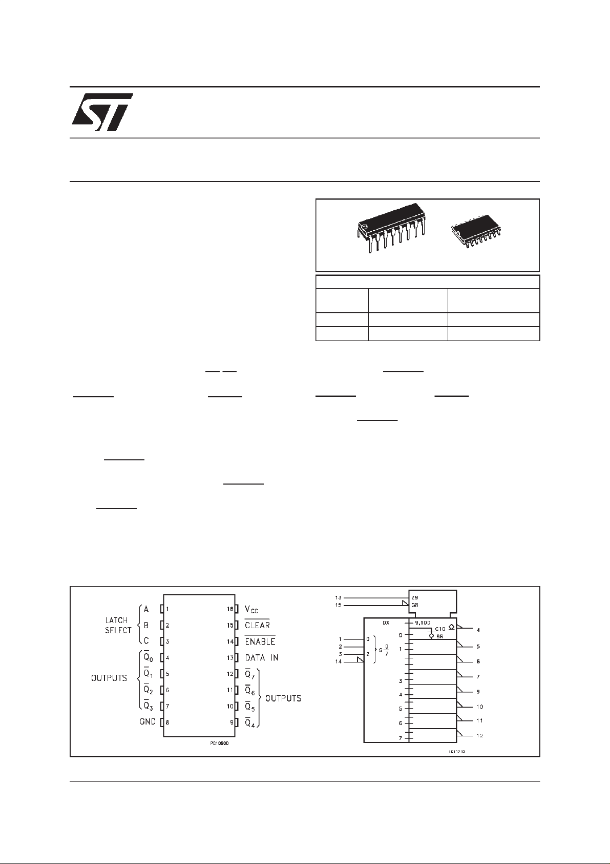
PIN CONNECTIONAND IEC LOGICSYMBOLS
February 2000
1/11
Page 2
M74HCT7259
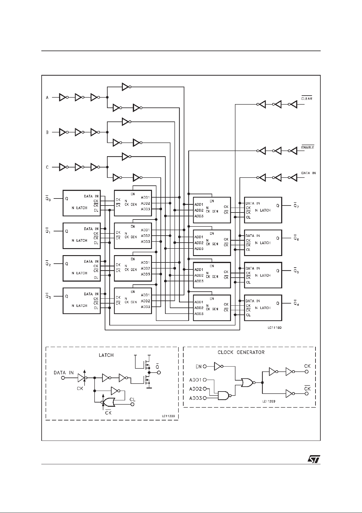
LOGICDIAGRAM
2/11
Page 3
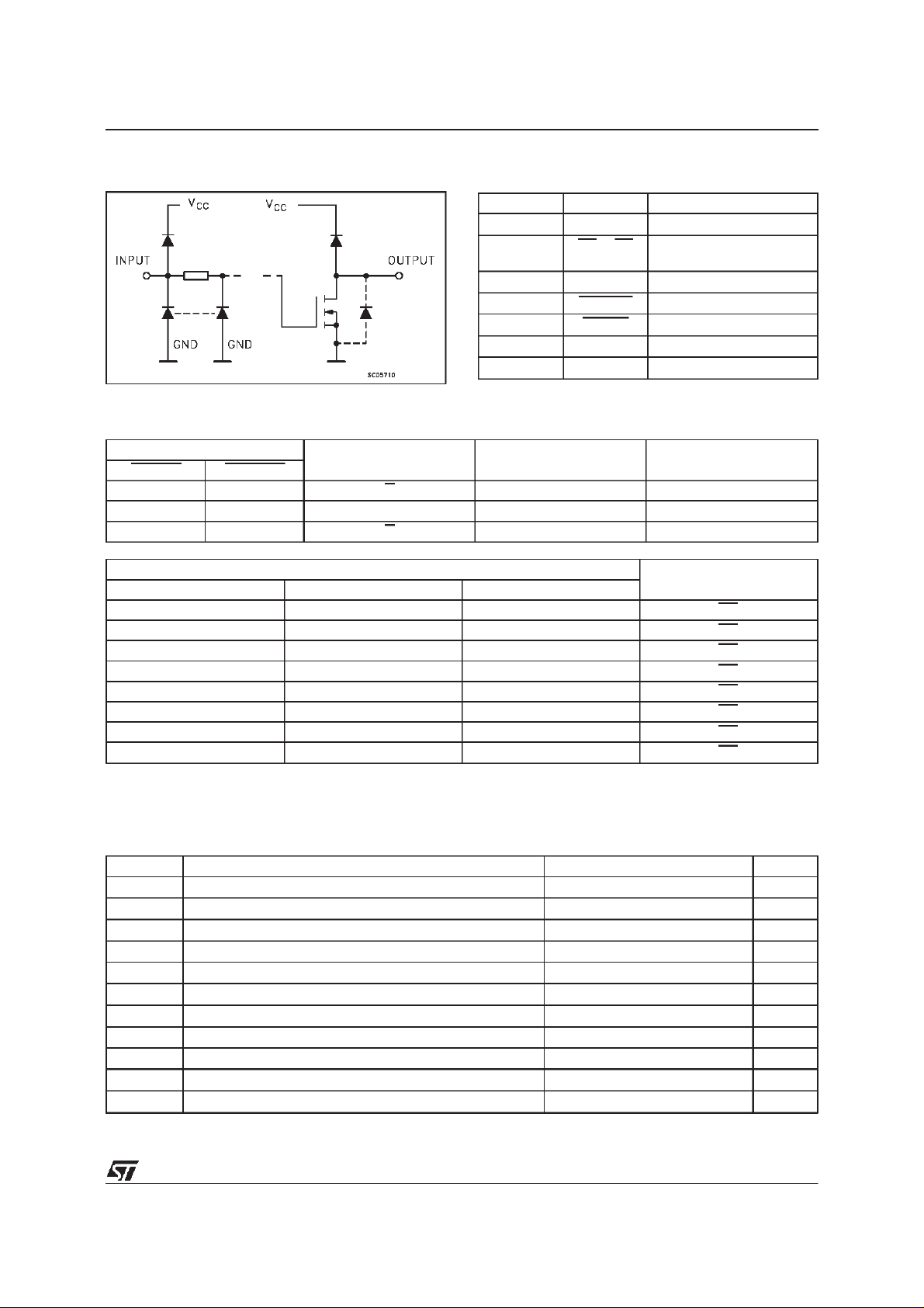
INPUT EQUIVALENTCIRCUIT PIN DESCRIPTION
PI N No SYMB OL NAME AND FUNCT IO N
1, 2, 3 A, B, C Latch Select
4, 5, 6, 7,9,
Q0 to Q7 latch Outputs
10, 11, 12
13 DATA IN Data Inputs
14 ENABLE Latch Enable Input
15 CLEAR Conditional Reset Input
8 GND Ground (0V)
16 V
TRUTH TABLE
CC
M74HCT7259
Positive Supply Voltage
INPUTS OUTPUTS OF
CLE AR ENABL E
ADDRESSED LA TCH
EAC H O THER O U T PUT FUNCTIO N
H L D QI0 ADDRESSABLE LATCH
H H Qi0 Qi0 MEMORY
L L D H 8-LINE DEMULTIPLEXER
SELE CT I NPUT S LAT CH ADDRESSED
CBA
LLLQ0
LLHQ1
LHLQ2
LHHQ3
HLLQ4
HLHQ5
HHLQ6
HHHQ7
D:The level atthedatainput
Qi0:The levelbeforetheindicate dsteady stateinpu tcond ition swereestablished ,(i = 0,1,....,7).
ABSOLUTE MAXIMUMRATINGS
Symb o l Para met er Val u e Uni t
V
V
V
I
I
OK
I
I
GND
I
CC
P
T
T
AbsoluteMaximumRatingsarethose values beyond whichdamageto thedevicemayoccur. Functionaloperation underthese condition isnotimplied.
(*)500mW:≅65
Supply Voltage -0.5 to +7.0 V
CC
DC Input Voltage -0.5 to VCC+ 0.5 V
I
DC Output Voltage -0.5 to VCC+ 0.5 V
O
DC Input Diode Current ± 20 mA
IK
DC Output Diode Current
DC Output Current Per Pin 100 mA
O
20 mA
±
Ground Current - 800 mA
DC VCCCurrent 50 mA
Power Dissipation 500 (*) mW
D
Storage Temperature -65 to +150
stg
Lead Temperature (10 sec) 300
L
o
Cderateto300mWby10mW/oC:65oCto85oC
o
C
o
C
3/11
Page 4
M74HCT7259
RECOMMENDEDOPERATINGCONDITIONS
Symb o l Para met er Value Un it
V
V
V
T
dt/dv Input Rise and Fall Time 0 to 500 ns
DC SPECIFICATIONS
Symbol Parameter Test Conditi ons Value Unit
V
IH
V
IL
V
OL
I
OZ
I
IN
I
CC
(*)VoltageRangeis3.3V±5%
Supply Voltage 3.3 to 5.5 V
CC
Input Voltage 0 to V
I
Output Voltage 0 to V
O
Operating Temperature -40 to +85
op
V
(V)
High Level Input Voltage 3.3
4.5
CC
(*)
T
A
Min. Typ. Max. Min. Max.
2.0 2.0
2.0 2.0
=25oC -40 to 85oC
CC
CC
to
5.5
4.5
(*)
0.5 0.5
0.8 0.8
Low Level Input Voltage 3.3
to
5.5
Low Level Output Voltage 3.3
Output Leackage Current
Input Leakage Current 5.5 VI=VCCorGND
Quiescent Supply Current
(*)
IO= 70 mA 0.4 0.5 0.6
=20µA 0.0 0.1 0.1
I
4.5
5.5
O
= 36 mA 0.17 0.26 0.33
I
O
= 80 mA 0.32 0.40 0.50
I
O
VI=VIHorV
V
OUT=VCC
IL
or GND
±5 ±50 µA
0.1
±
VI=VCCorGND 4 40
Each Input in Turn:
5.5
= 0.5 V or2.4 V
V
IN
All Other Inputs:
V
orGND
CC
3.0 3.9 mA
V
V
o
C
1
±
µ
µ
V
V
V
A
A
4/11
Page 5

M74HCT7259
AC ELECTRICALCHARACTERISTICS
= 50 pF, Input tr=tf=6 ns)
(C
L
Symb o l Parameter Test Condit io ns Val ue Unit
Output Transition Time 3.3
t
TLH
Propagation Delay Time
t
PLZ
t
(DATA - Q)
PZL
C
V
CC
(V)
(pF)
(*)
50 1 18
4.5 50 1 3 6 9
(*)
3.3
50 1 80
(*)
150 1 92
3.3
R
L
L
(KΩ)
T
=25oC -40 to 85oC
A
Min. Typ. Max. Min. Max.
ns
ns
4.5 50 1 20 31 39
4.5 150 1 24 37 46
Propagation Delay Time
t
PLZ
t
(A, B, C - Q)
PZL
(*)
3.3
50 1 98
(*)
150 1 112
3.3
ns
4.5 50 1 25 39 49
4.5 150 1 29 45 56
Propagation Delay Time
t
PLZ
(ENABLE - Q)
t
PZL
(*)
3.3
50 1 82
(*)
150 1 98
3.3
ns
4.5 50 1 21 33 41
4.5 150 1 25 39 49
Propagation Delay Time
t
PLZ
t
(CLEAR - Q)
PZL
(*)
3.3
50 1 76
(*)
150 1 90
3.3
ns
4.5 50 1 19 30 38
4.5 150 1 23 36 45
t
t
C
PD
(*)VoltageRangeis3.3V±5%
(**) C
toTestCircuit).Average opertingcurrent canbeobtainedby thefollowingequation.I
Minimum Pulse Width (CLEAR) 3.3
W(L)
Minimum Pulse Width (ENABLE) 3.3
W(L)
Minimum Set-Up Time 3.3
t
s
Minimum Hold Time 3.3
t
h
Input Capacitance 5 10 10
C
IN
(**) Power Dissipation Capacitance 96 pF
isdefined asthevalueoftheIC’sinternal equivalent capacitance whichiscalculatedfromtheoperatingcurrent consumptionwithoutload.(Refer
PD
(*)
50 1 38
4.5 50 1 7 15 19
(*)
50 1 38
4.5 50 1 7 15 19
(*)
50 1 26
4.5 50 1 4 10 13
(*)
50 1 10
4.5 50 1 5 5
V
(opr)=C
CC
PD
f
•
•
CC
IN+ICC
ns
ns
ns
ns
pF
5/11
Page 6

M74HCT7259
SWITCHING CHARACTERISTICS TEST WAVEFORMS
WAVEFORM1: (ENABLE =L, CLR = H, A-C=STABLE)
WAVEFORM2: (ENABLE =L)
6/11
Page 7

WAVEFORM3: (CLR = H, A-C = STABLE)
M74HCT7259
WAVEFORM4: (D = H, A-C = STABLE)
7/11
Page 8

M74HCT7259
WAVEFORM5: (CLR = H)
TESTCIRCUIT I
CC
(Opr.)
8/11
Page 9

Plastic DIP-16 (0.25) MECHANICAL DATA
M74HCT7259
DIM.
MIN. TYP. MAX. MIN. TYP. MAX.
a1 0.51 0.020
B 0.77 1.65 0.030 0.065
b 0.5 0.020
b1 0.25 0.010
D 20 0.787
E 8.5 0.335
e 2.54 0.100
e3 17.78 0.700
F 7.1 0.280
I 5.1 0.201
L 3.3 0.130
Z 1.27 0.050
mm inch
P001C
9/11
Page 10

M74HCT7259
SO16L MECHANICAL DATA
DIM.
MIN. TYP. MAX. MIN. TYP. MAX.
A 2.65 0.104
a1 0.1 0.2 0.004 0.008
a2 2.45 0.096
b 0.35 0.49 0.014 0.019
b1 0.23 0.32 0.009 0.012
C 0.5 0.020
c1 45 (typ.)
D 10.1 10.5 0.397 0.413
E 10.0 10.65 0.3.93 0.419
e 1.27 0.050
e3 8.89 0.350
F 7.4 7.6 0.291 0.300
L 0.5 1.27 0.020 0.050
M 0.75 0.029
S 8 (max.)
mm inch
10/11
P013I
Page 11

M74HCT7259
Information furnished isbelieved tobe accurate and reliable. However, STMicroelectronics assumes no responsibility forthe consequences
of use of such information nor for any infringement of patents or other rights of third parties which may result from its use. No license is
granted by implication or otherwise under any patent or patent rights of STMicroelectronics. Specification mentioned in this publication are
subject tochange without notice. Thispublication supersedes andreplaces all information previously supplied. STMicroelectronics products
are notauthorized for use as critical components in lifesupport devices or systems withoutexpress written approval of STMicroelectronics.
The STlogo is a registeredtrademark of STMicroelectronics
2000 STMicroelectronics – Printedin Italy – All Rights Reserved
STMicroelectronics GROUP OF COMPANIES
Australia - Brazil - China - Finland - France - Germany - Hong Kong - India - Italy - Japan- Malaysia -Malta - Morocco
Singapore - Spain- Sweden - Switzerland - UnitedKingdom - U.S.A.
http://www.st.com
.
11/11
 Loading...