

Page 1

.HIGH SPEED
tPD= 17 ns(TYP.) AT VCC=5V
.LOWPOWER DISSIPATION
ICC=4µA(MAX.) AT TA=25°C
.COMPATIBLE WITH TTL OUTPUTS
VIH= 2V (MIN.) VIL= 0.8V (MAX)
.OUTPUT DRIVE CAPABILITY
10 LSTTLLOADS
.SYMMETRICALOUTPUT IMPEDANCE
|IOH|=IOL= 4 mA (MIN.)
.BALANCEDPROPAGATION DELAYS
t
PLH=tPHL
.PIN ANDFUNCTION COMPATIBLE
WITH 54/74LS688
M54HCT688
M74HCT688
8 BITEQUALITY COMPARATOR
B1R
(PlasticPackage)
M1R
(MicroPackage)
ORDER CODES :
M54HC T688F1R M74H CT688M1R
M74HC T688B1R M74HCT688C1R
F1R
(CeramicPackage)
C1R
(Chip Carrier)
DESCRIPTION
The M54/74HCT688 utilizes silicon gate C2MOS
technology to achieve operating speeds equivalent
to LSTTL devices. Along with the low power
dissipation and high noise immunity of standard
C2MOS integrated circuit, it possesses the driving
capability of 10 LSTTL load. The M54/74HCT688
compares bitforbittwo8-bit wordsapplied oninputs
P0 - P7 and inputs Q0 - Q7 and indicates whether
or not they are equal. A single active lowenable is
provided to facilitate cascading severalpackagesto
enablecomparison of wordsgreater than 8 bits.
This integrated circuit has input and output
characteristics that are fully compatible with 54/74
LSTTL logic families. M54/74HCT devices are
designed to directly interface HSC2MOS systems
with TTL and NMOS components. They are also
plug in replacements for LSTTL devices giving a
reduction ofpower consumption.
All inputs are equipped with protection circuit
against static discharge and transient excess
voltage.
PIN CONNECTIONS(top view)
NC =
No Internal
Connection
February 1993
1/10
Page 2
M54/M74HCT688
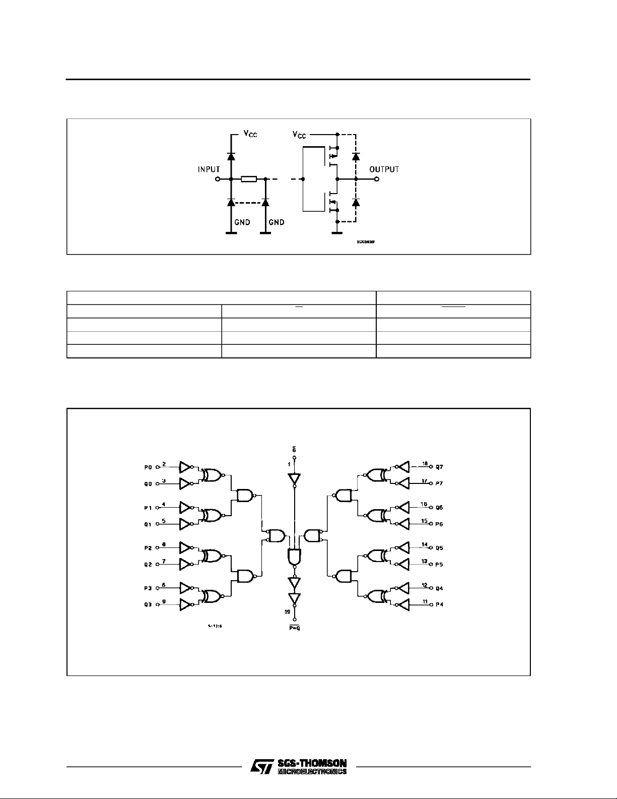
INPUT AND OUTPUT EQUIVALENT CIRCUIT
TRUTH TABLE
INPUT OUTPUT
P, Q G P = Q
P=Q L L
P≠QL H
XHH
X:DON’T CARE
LOGIC DIAGRAM
2/10
Page 3
M54/M74HCT688
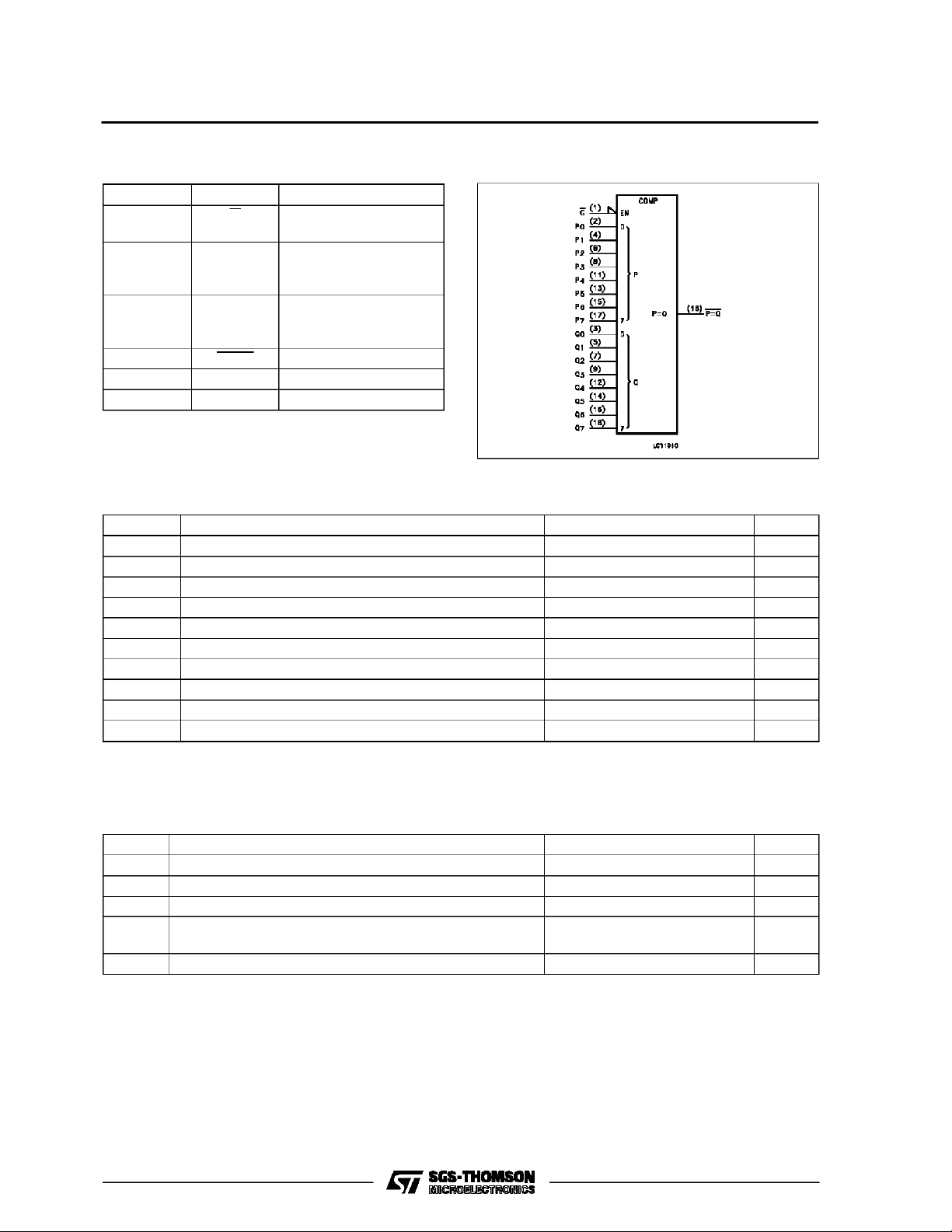
PIN DESCRIPTION
IEC LOGIC SYMBOL
PIN No SYMBOL NAME AND FUNCTION
1 G Enable Input (Active
LOW)
2, 4, 6, 8,
P0 to P7 Word Inputs
11, 13, 15,
17
3, 5, 7, 9,
Q0 to Q7 Word Outputs
12, 14, 16,
18
19 P = Q Equal to Output
10 GND Ground (0V)
20 V
CC
Positive Supply Voltage
ABSOLU TE MAXIMU M RAT ING S
Symbol Parameter Value Unit
V
CC
V
V
O
I
IK
I
OK
I
O
or I
I
CC
P
D
T
stg
T
AbsoluteMaximumRatingsarethosevaluesbeyondwhichdamage tothedevicemayoccur.Functionaloperationunder theseconditionisnotimplied.
(*)500 mW:≅ 65oC derateto 300 mWby 10mW/oC: 65oCto85oC
Supply Voltage -0.5 to +7 V
DC Input Voltage -0.5 to VCC+ 0.5 V
I
DC Output Voltage -0.5 to VCC+ 0.5 V
DC Input Diode Current ± 20 mA
DC Output Diode Current ± 20 mA
DC Output Source Sink Current Per Output Pin ± 25 mA
DC VCCor Ground Current ± 50 mA
GND
Power Dissipation 500 (*) mW
Storage Temperature -65 to +150
Lead Temperature (10 sec) 300
L
o
C
o
C
RECO MM ENDED OPERATIN G CONDI TI O NS
Symbol Parameter Value Unit
V
T
t
V
V
r,tf
Supply Voltage 4.5 to 5.5 V
CC
Input Voltage 0 to V
I
Output Voltage 0 to V
O
Operating Temperature: M54HC Series
op
M74HC Series
CC
CC
-55 to +125
-40 to +85
Input Rise and Fall Time (VCC= 4.5 to 5.5V) 0 to 500 ns
V
V
o
C
o
C
3/10
Page 4

M54/M74HCT688
DC SPECIFICATIO NS
Symbol Parameter
V
V
V
V
I
∆I
High Level Input
IH
Voltage
Low Level Input
IL
Voltage
High Level
OH
Output Voltage
Low Level Output
OL
Voltage
Input Leakage
I
I
Current
Quiescent Supply
CC
Current
Additional worst
CC
case supply
current
Test Conditions Value
V
(V)
4.5
CC
=25oC
A
54HC and 74HC
Min. Typ. Max. Min. Max. Min. Max.
2.0 2.0 2.0 V
-40 to 85oC
74HC
-55 to 125oC
54HC
Unit
T
to
5.5
4.5
0.8 0.8 0.8 V
to
5.5
VI=
IO=-20 µA 4.4 4.5 4.4 4.4
V
IH
4.5
or
I
=-4.0 mA 4.18 4.31 4.13 4.10
O
V
IL
VI=
IO=20µA 0.0 0.1 0.1 0.1
V
IH
4.5
or
I
= 4.0 mA 0.17 0.26 0.33 0.4
O
V
IL
VI=VCCor GND ±0.1 ±1 ±1 µA
5.5
5.5 VI=VCCor GND 4 40 80 µA
5.5 Per Input pin
2.0 2.9 3.0 mA
VI= 0.5V or
V
= 2.4V
I
Other Inputs at
VCCor GND
V
V
4/10
Page 5

M54/M74HCT688
AC ELECTRICAL CHARACTERISTICS (CL=50pF,Inputtr=tf=6ns)
Test Conditions Value
T
=25oC
Symbol Parameter
t
t
t
t
TLH
THL
PLH
PHL
Output Transition
Time
Propagation
Delay Time
V
CC
(V)
4.5 8151922
4.5 21 32 40 48
A
54HC and 74HC
Min. Typ. Max. Min. Max. Min. Max.
(Pn, Qn - P = Q)
t
t
PLH
PHL
Propagation
Delay Time
4.5 15 23 29 35
(G - P = Q)
C
C
PD
Input Capacitance 5 10 10 10 pF
IN
(*) Power Dissipation
32
Capacitance
(*) CPDisdefined as the valueof the IC’s internal equivalent capacitance which is calculatedfromthe operatingcurrent consumption withoutload.
(Referto Test Circuit).Average opertingcurrent can be obtained bythefollowingequation. ICC(opr) = CPD•VCC•fIN+I
-40 to 85oC
74HC
-55 to 125oC
54HC
CC
Unit
ns
ns
ns
pF
SWITCHING CHARACTERISTICS TEST
WAVEFORM
TEST CIRCUIT ICC (Opr.)
INPUT WAVEFORM IS THE SAME AS THAT IN CASE OF
SWITCHINGCHARACTERISTICSTEST.
5/10
Page 6

M54/M74HCT688
Plastic DIP20 (0.25) MECHANICAL DATA
DIM.
MIN. TYP. MAX. MIN. TYP. MAX.
a1 0.254 0.010
B 1.39 1.65 0.055 0.065
b 0.45 0.018
b1 0.25 0.010
D 25.4 1.000
E 8.5 0.335
e 2.54 0.100
e3 22.86 0.900
F 7.1 0.280
I 3.93 0.155
L 3.3 0.130
Z 1.34 0.053
mm inch
6/10
P001J
Page 7

Ceramic DIP20 MECHANICAL DATA
M54/M74HCT688
DIM.
MIN. TYP. MAX. MIN. TYP. MAX.
A 25 0.984
B 7.8 0.307
D 3.3 0.130
E 0.5 1.78 0.020 0.070
e3 22.86 0.900
F 2.29 2.79 0.090 0.110
G 0.4 0.55 0.016 0.022
I 1.27 1.52 0.050 0.060
L 0.22 0.31 0.009 0.012
M 0.51 1.27 0.020 0.050
N1 4° (min.), 15° (max.)
P 7.9 8.13 0.311 0.320
Q 5.71 0.225
mm inch
P057H
7/10
Page 8

M54/M74HCT688
SO20 MECHANICAL DATA
DIM.
MIN. TYP. MAX. MIN. TYP. MAX.
A 2.65 0.104
a1 0.10 0.20 0.004 0.007
a2 2.45 0.096
b 0.35 0.49 0.013 0.019
b1 0.23 0.32 0.009 0.012
C 0.50 0.020
c1 45° (typ.)
D 12.60 13.00 0.496 0.512
E 10.00 10.65 0.393 0.419
e 1.27 0.050
e3 11.43 0.450
F 7.40 7.60 0.291 0.299
L 0.50 1.27 0.19 0.050
M 0.75 0.029
S8°(max.)
mm inch
8/10
P013L
Page 9

PLCC20 MECHANICAL DATA
M54/M74HCT688
DIM.
MIN. TYP. MAX. MIN. TYP. MAX.
A 9.78 10.03 0.385 0.395
B 8.89 9.04 0.350 0.356
D 4.2 4.57 0.165 0.180
d1 2.54 0.100
d2 0.56 0.022
E 7.37 8.38 0.290 0.330
e 1.27 0.050
e3 5.08 0.200
F 0.38 0.015
G 0.101 0.004
M 1.27 0.050
M1 1.14 0.045
mm inch
P027A
9/10
Page 10

M54/M74HCT688
Information furnished is believed to be accurate and reliable. However, SGS-THOMSON Microelectronics assumes no responsability for the
consequences of use of such information nor for any infringement of patents or other rights of third partieswhich may results from its use. No
license is granted byimplication or otherwise under any patent or patentrights of SGS-THOMSON Microelectronics. Specificationsmentioned
in this publication are subject to change without notice. This publication supersedes and replaces all information previously supplied.
SGS-THOMSON Microelectronicsproducts are not authorized foruse ascritical componentsin life support devices or systems without express
written approval of SGS-THOMSON Microelectonics.
1994 SGS-THOMSON Microelectronics - All Rights Reserved
Australia - Brazil - France - Germany - Hong Kong - Italy - Japan - Korea- Malaysia - Malta -Morocco - The Netherlands -
Singapore -Spain - Sweden- Switzerland - Taiwan - Thailand - UnitedKingdom - U.S.A
SGS-THOMSON Microelectronics GROUP OF COMPANIES
10/10
 Loading...