

Page 1
M74HCT646
M74HCT648
HCT646 OCTAL BUS TRANSCEIVER/REGISTER (3-STATE)
HCT648 OCTAL BUS TRANSCEIVER/REGISTER (3-STATE, INV.)
.HIGH SPEED
f
= 60 MHz(TYP.) AT VCC=5V
MAX
.LOWPOWERDISSIPATION
ICC=4µA(MAX.) AT TA=25°C
.COMPATIBLE WITHTTL OUTPUTS
VIH= 2V (MIN.)VIL= 0.8V (MAX)
.OUTPUT DRIVE CAPABILITY
15 LSTTL LOADS
B1R
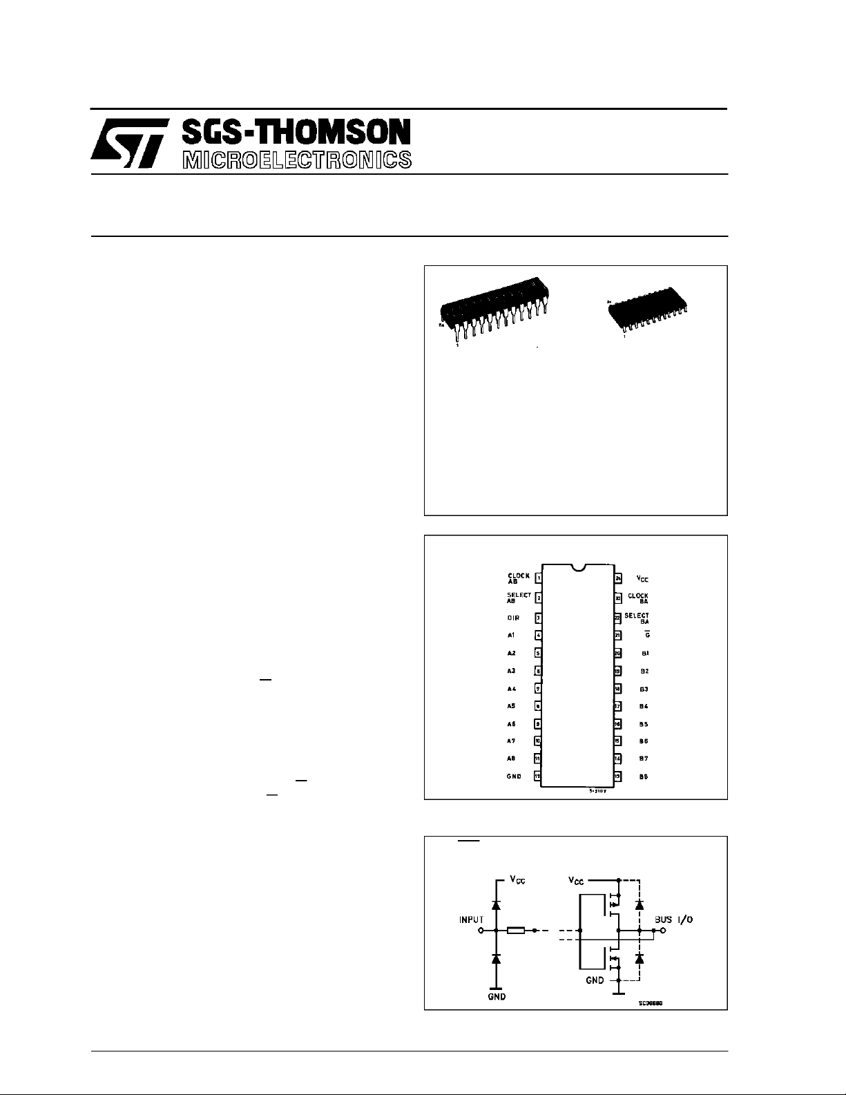
(PlasticPackage)
M1R
(Micro Package)
.SYMMETRICALOUTPUT IMPEDANCE
IOH=IOL=6 mA(MIN.)
.BALANCEDPROPAGATION DELAYS
t
PLH=tPHL
.PIN ANDFUNCTION COMPATIBLE
WITH 54/74LS646/648
DESCRIPTION
The M74HCT646/648 are high speed CMOS
OCTALBUS TRANSCEIVERS AND REGISTERS,
(3-STATE) fabricated in silicon gate C2MOS technology. They have the same high speed
performance of LSTTL combined with true CMOS
low power consumption. These devices consist of
bus transceiver circuits with 3-state output, D-type
flip-flops, and control circuitry arranged for multiplexed transmission of data directly from the input
bus or from the internal registers. Data on the A or
B bus will be clocked into the registers on thelowto-high transition of theappropriate clock pin (Clock
AB - or Clock BA). Enable (G) and direction (DIR)
pinsare providedtocontrolthe transceiverfunctions. In the transceiver mode, data present at the
high-impedanceportmay bestoredineitherregister
or inboth. Theselectcontrols (Select AB select BA)
can multiplex stored and real-time (transparent
mode)data. Thedirectioncontroldetermines which
bus willreceive data when enableG is active(low).
In theisolation mode (enable G high),”A” data may
be stored in one register and/or ”B” data may be
storedinthe otherregister.Whenanoutputfunction
is disabled, the input function is still enabled and
may be used to store and transmit data. Only one
of the two buses, A or B, may be driven at a time.
All inputs are equipped with protection circuits
against static discharge and transient excess voltage.This integrated circuit has input and output
characteristics that are fully compatible with 54/74
LSTTL logic families. M74HCT devices are designedto directly interfaceHSC2MOSsystemswith
TTLand NMOScomponents. Theyare also plug in
replacements for LSTTL devices giving areduction
of power consumption.
M74HC TXXXM1R M74H CTXX XB1R
PIN CONNECTIONS (top view)
INPUT AND OUTPUT EQUIVALENT CIRCUIT
GAB,GAB,CAB, A, B
SAB,SBA, CBA
ORDER CODES :
October 1993
1/12
Page 2
M74HCT646/648
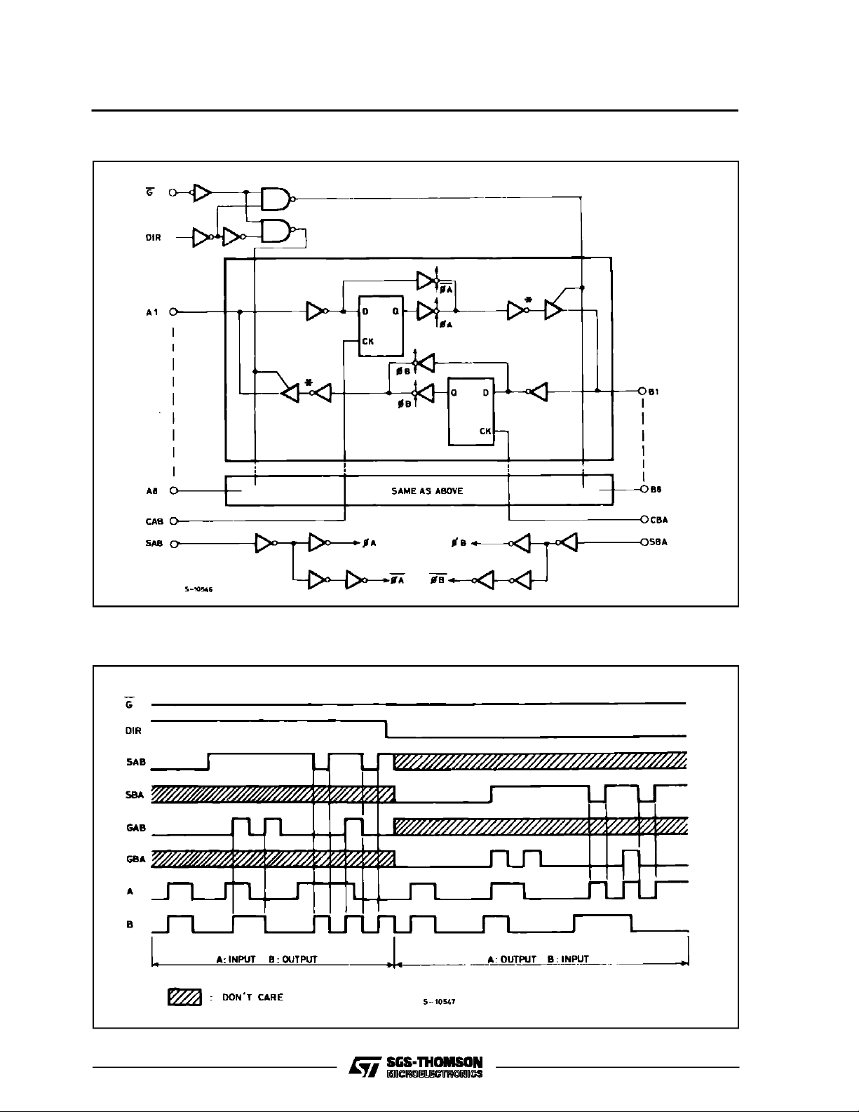
LOGIC DIAGRAM (HCT648)
Note: In case ofM54/74HCT646 output invertermarked *at A bus and B bus areeliminated.
TIMING CHART
2/12
Page 3
M74HCT646/648
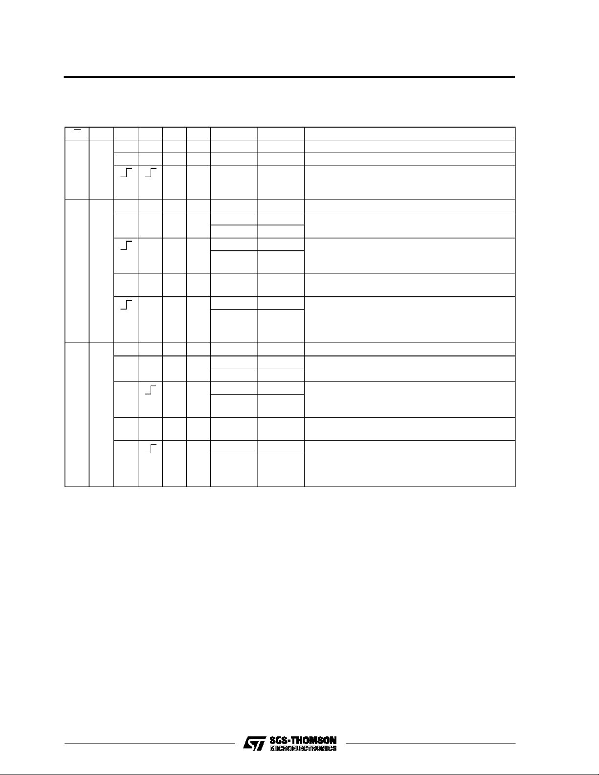
TRUTH TABLE
HCT646 (The trut h table for HCT64 8 is th e same as t his, but w i th t he o ut put s inver t ed)
G DIR CAB CBA SAB SBA A B FUNCTION
INPUTS INPUTS Both the A bus and the B bus are inputs
HX
LH
LL
X : DON’TCARE
Z :HIGH IMPEDANCE
Qn :THE DATA STOREDTO THE INTERNALFLIP-FLOPS BY MOST RECENT LOW TO HIGHTRANSITIONOF THE CLOCK INPUTS
* : THEDATA AT THE A ANDB BUSWILLBE STOREDTO THE INTERNALFLIP-FLOPSONEVERY LOW TO HIGH TRANSITIONOF
THECLOCK INPUTS
X X X X Z Z The output functions of the A and B bus are disabled
X X INPUTS INPUTS Both the A and B bus are used for inputs to the
internal flip-flops. Data at the bus will be stored on
low to high transition of the clock inputs
iNPUTS OUTPUTS The A bus are inputs and the B bus are outputs
X X* L X L L The data at the A bus are displayed at the B bus
HH
X* L X L L The data at the A bus are displayed at the B bus.
HH
The data of the A bus are stored to the internal
flip-flop on low to high transition of th clock pulse.
X X* H X X Qn The data stored to the internal flip-flop are dispayed
at the B bus
X* H X L L The data at the A bus are stored to the internal flip-
HH
flop on low to high transition of the clock pulse. The
states of the internal flip-flops output directly to the
B bus
OUTPUTS INPUTS The A bus are outputs and the B bus are inputs
X* X X L
L L The data at the B bus are displayed at the A bus
HH
X* X L L L The data at the B bus are displayed at the A bus.
HH
The data of the B bus are stored to the internal flipflop on low to high transition of the clock pulse
X* X X H Qn X The data stored to the internal flip-flops are
displayed at the B bus
x* X H L L the data at the B bus are stored to the internal flip-
HH
flop on low to high transition of the clock pulse. The
states of the internal flip-flops output directly to the
A bus
3/12
Page 4
M74HCT646/648
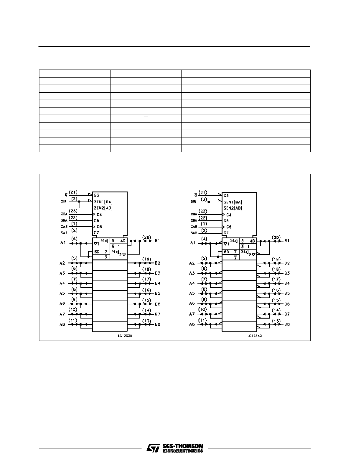
PIN DESCRIPTION
PIN No SYMBOL NAME AND FUNCTION
1 CLOCK AB A to B Clock Input (LOW to HIGH, Edge-Trigged)
2 SELECT AB Select A to B Source Input
3 DIR Direction Control Input
4, 5, 6, 7, 8, 9, 10, 11 A1 to A8 A data Inputs/Outputs
20, 19, 18, 17, 16, 15, 14, 13 B1 to B8 B Data Inputs/Outputs
21 G Output Enable Input (Active LOW)
22 SELECT BA Select B to A Source Input
23 CLOCK BA B to A Clock Input (LOW to HIGH, Edge-Triggered)
12 GND Ground (0V)
24 V
IEC LOGIC SYMBOLS
CC
HCT646 HCT648
Positive Supply Voltage
4/12
Page 5

M74HCT646/648
ABSOLU TE M AXI MUM RATINGS
Symbol Parameter Value Unit
V
CC
V
V
O
I
IK
I
OK
I
O
I
or I
CC
P
D
T
stg
T
AbsoluteMaximumRatingsarethose values beyondwhichdamage tothedevicemayoccur. Functional operationunder these conditionisnotimplied.
(*)500 mW: ≅ 65oC derateto300 mWby 10mW/oC: 65oCto85oC
RECO MM ENDED OPERAT IN G CONDI TI O NS
Symbol Parameter Value Unit
V
CC
V
I
V
O
T
op
t
r,tf
Supply Voltage -0.5 to +7 V
DC Input Voltage -0.5 to VCC+ 0.5 V
I
DC Output Voltage -0.5 to VCC+ 0.5 V
DC Input Diode Current ± 20 mA
DC Output Diode Current ± 20 mA
DC Output Source Sink Current Per Output Pin ± 35 mA
DC VCCor Ground Current ± 70 mA
GND
Power Dissipation 500 (*) mW
Storage Temperature -65 to +150
Lead Temperature (10 sec) 300
L
Supply Voltage 4.5 to 5.5 V
Input Voltage 0 to V
Output Voltage 0 to V
CC
CC
Operating Temperature -40 to +85
Input Rise and Fall Time (VCC= 4.5 to 5.5V) 0 to 500 ns
o
C
o
C
V
V
o
C
5/12
Page 6

M74HCT646/648
DC SPECIFICATIONS
Symbol Parameter
V
V
V
V
I
I
∆I
(*):Applicable onlyto DIR, G, CAB,CBA, SBAinput.
High Level Input Voltage 4.5
IH
Low Level Input
IL
Voltage
High Level Output Voltage
OH
Low Level Output Voltage
OL
Input Leakage Current (*) 5.5 VI=VCCor GND ±0.1 ±1 µA
I
I
Quiescent Supply Current 5.5 VI=VCCor GND 4 40 µA
CC
Output Off-state Current 5.5 VO=VCCor GND
OZ
Additional worst case supply
CC
current
Test Conditions Value
V
(V)
CC
TA=25oC -40 to 85oC
Min. Typ. Max. Min. Max.
2.0 2.0 V
to
5.5
4.5
to
5.5
VI=
IO=-20 µA 4.4 4.5 4.4
V
IH
I
=-6.0 mA 4.18 4.31 4.13
4.5
4.5
O
or
V
IL
VI=
IO=20µA 0.0 0.1 0.1
V
IH
I
= 6.0 mA 0.17 0.26 0.33
O
or
V
IL
VI=VIHor V
IL
5.5 Per Input pin
VI= 0.5V or
VI= 2.4V
Other Inputs at
VCCor GND
IO=0
Unit
0.8 0.8 V
V
V
æ0.5 ±5 µA
2.0 2.9 mA
6/12
Page 7

M74HCT646/648
AC ELECTRICAL CHARACTERISTICS (CL=50pF,Inputtr=tf=6ns)
Test Conditions Value
T
=25oC
Symbol Parameter
t
TLH
t
THL
t
PLH
t
PHL
t
PLH
t
PHL
t
PLH
t
PHL
t
PZL
t
PZH
t
PLZ
t
PHZ
f
MAX
t
W(H)
t
W(L)
C
C
C
PD
Output Transition Time 4.5 50 7 12 15
Propagation Delay Time
(BUS - BUS)
Propagation Delay Time
(CLOCK - BUS)
Propagation Delay Time
(SELECT - BUS)
3-State Output Enable Time
(G, DIR - BUS)
3-State Output Disable Time
(G, DIR - BUS)
Maximum Clock Frequency 4.5 50 31 55 25 MHz
Minimum Pulse Width 4.5 50 8 15 19 ns
Minimum Set-up Time 4.5 50 3 10 13 ns
t
s
Minimum Hold Time 4.5 50 5 5 ns
t
h
Input Capacitance 5 10 10 pF
IN
Bus Terminal Capacitance 13 pF
I/O
(*) Power Dissipation Capacitance for HCT646
V
C
CC
(V)
L
(pF)
4.5 50 20 30 38 ns
4.5 150 25 38 48 ns
4.5 50 29 44 55 ns
4.5 150 34 52 65 ns
4.5 50 24 34 43 ns
4.5 150 29 42 53 ns
4.5 50 RL=1KΩ 26 38 48 ns
4.5 150 R
=1KΩ 31 46 58 ns
L
4.5 50 RL=1KΩ 26 35 44 ns
for HCT648
(*) CPDisdefined as the value ofthe IC’sinternal equivalent capacitance which is calculated fromthe operatingcurrent consumption without load.
(Referto Test Circuit). Average operting current canbe obtained bythe followingequation. ICC(opr) = CPD•VCC•fIN+ICC/8(per bit)
A
54HC and 74HC
Min. Typ. Max. Min. Max.
40
39
-40 to 85oC
74HC
Unit
ns
pF
7/12
Page 8

M74HCT646/648
SWITCHING CHARACTERISTICS TEST CIRCUIT AND WAVEFORM
WAVEFORM 1 WAVEFORM 2
WAVEFORM 3 WAVEFORM 4
8/12
WAVEFORM 5
Page 9

TEST WAVEFORM ICC(Opr.)
* INPUTTRANSITION TIMEIS THE SAME AS THATIN CASEOF SWITCHINGCHARACTERISTICSTEST.
M74HCT646/648
9/12
Page 10

M74HCT646/648
Plastic DIP24 (0.25) MECHANICAL DATA
DIM.
MIN. TYP. MAX. MIN. TYP. MAX.
a1 0.63 0.025
b 0.45 0.018
b1 0.23 0.31 0.009 0.012
b2 1.27 0.050
D 32.2 1.268
E 15.2 16.68 0.598 0.657
e 2.54 0.100
e3 27.94 1.100
F 14.1 0.555
I 4.445 0.175
L 3.3 0.130
mm inch
10/12
P043A
Page 11

SO24 MECHANICAL DATA
M74HCT646/648
DIM.
MIN. TYP. MAX. MIN. TYP. MAX.
A 2.65 0.104
a1 0.10 0.20 0.004 0.007
a2 2.45 0.096
b 0.35 0.49 0.013 0.019
b1 0.23 0.32 0.009 0.012
C 0.50 0.020
c1 45° (typ.)
D 15.20 15.60 0.598 0.614
E 10.00 10.65 0.393 0.420
e 1.27 0.05
e3 13.97 0.55
F 7.40 7.60 0.291 0.299
L 0.50 1.27 0.19 0.050
S8°(max.)
mm inch
L
A
a2
b
e3
D
24 13
112
e
F
s
a1
c1
b1
C
E
11/12
Page 12

M74HCT646/648
Information furnishedis believed to be accurate and reliable. However, SGS-THOMSON Microelectronicsassumes no responsability for the
consequences of useof suchinformation nor for any infringement of patents or other rights of third parties which may results from its use. No
license is granted byimplication or otherwiseunder any patentor patentrights ofSGS-THOMSON Microelectronics.Specificationsmentioned
in thispublication are subjectto changewithout notice. This publication supersedes andreplaces all information previouslysupplied.
SGS-THOMSON Microelectronicsproducts are not authorized foruse ascritical componentsinlife supportdevices or systems without express
written approval of SGS-THOMSON Microelectonics.
1994SGS-THOMSON Microelectronics- All Rights Reserved
Australia -Brazil - France - Germany - Hong Kong - Italy -Japan - Korea - Malaysia - Malta -Morocco - The Netherlands-
Singapore -Spain - Sweden- Switzerland - Taiwan - Thailand- UnitedKingdom - U.S.A
SGS-THOMSON Microelectronics GROUP OFCOMPANIES
12/12
 Loading...