

Page 1
M54/74HCT245/640/643
M54/74HCT245/640/643
OCTAL BUS TRANSCEIVER (3-STATE): HCT245 NON INVERTING
HCT640 INVERTING, HCT643 INVERTING/NON INVERTING
.HIGH SPEED
tPD= 10 ns(TYP.) at VCC=5V
.LOWPOWERDISSIPATION
ICC=4µA (MAX.) at TA=25oC
.COMPATIBLE WITHTTL OUTPUTS
VIH= 2V (MIN.)VIL= 0.8V (MAX.)
.OUTPUT DRIVE CAPABILITY
15 LSTTL LOADS
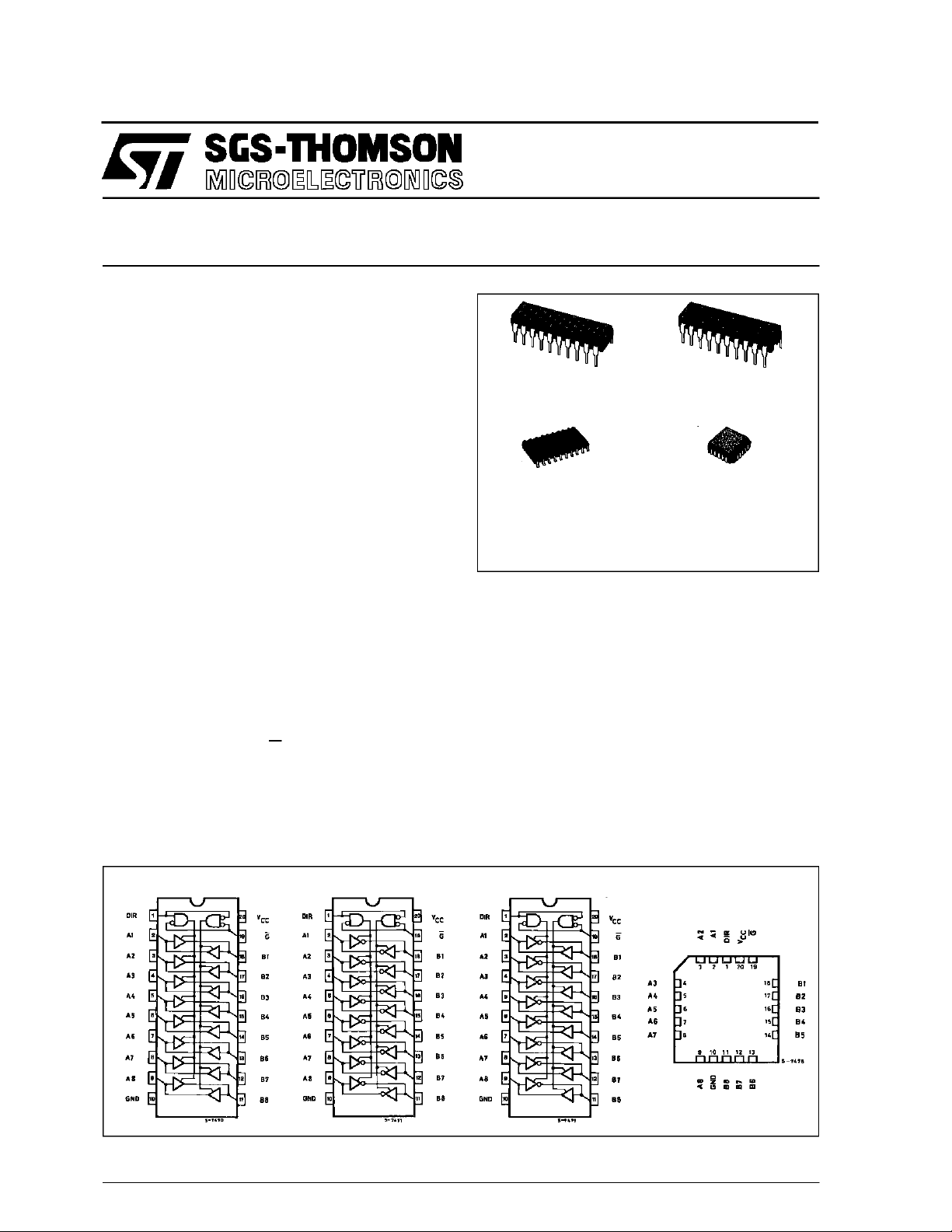
B1R
(PlasticPackage)
F1R
(CeramicPackage)
.SYMMETRICALOUTPUT IMPEDANCE
|IOH|=IOL=6 mA(MIN)
.BALANCEDPROPAGATION DELAYS
t
PLH=tPHL
.PIN ANDFUNCTION COMPATIBLE
WITH 54/74LS245/640/643
DESCRIPTION
The M54/74HCT245, HCT640 and HCT643 utilise
silicongate C2MOS technology toachive operating
speedseqivalent to LSTTL devices.
Alongwith thelow power dissipationandhighnoise
immunity of standad CMOS integrated circuit, it
possesses the capability to drive 15 LSTTL loads.
TheseIC’s are intended fortwo-way asynchronous
communication between data buses, and the
direction of data trasmission is determined by DIR
input. The enable input (G) can be usedto disable
the device sothatthe busesare effectively isolated.
All input are equipped with protection circuits
against static discharge and transient discharge.
These integrated circuits have input and output
characteristics that are fully compatible with 54/74
LSTTL logic families. M54/74HCT devices are
designed to directly interface HSC2MOS systems
with TTL and NMOS components. They are also
plug in replacements for LSTTL devices giving a
reduction of powerconsumption.
IT IS PROHIBITED TO APPLY A SIGNAL TO A
BUS TERMINAL WHEN IT IS IN OUTPUT MODE
AND WHEN A BUS THERMINAL IS FLOATING
(HIGH IMPEDANCE STATE), IT IS REQUESTED
TO FIX THE INPUT LEVEL BY MEANS OF
EXTERNAL PULL DOWN OR PULL UP
RESISTOR.
M1R
(MicroPackage)
ORDER CODE S :
M54HC TXX X F1R M74HC TXX X M1R
M74HC TXXXB1 R M7 4HCT XXXC1 R
C1R
(Chip Carrier)
PIN CONNECTION (top view)
HCT245 HCT640 HCT643
October 1993
1/11
Page 2
M54/M74HCT245/640/643
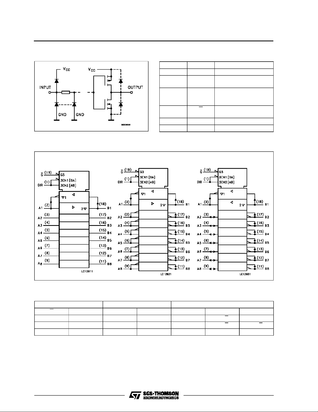
INPUT AND OUTPUT EQUIVALENT CIRCUIT PIN DESCRIPTION
PIN No SYMBOL NAME AND FUNCTION
1 DIR Directional Control
2, 3, 4, 5,
6, 7, 8, 9
18, 17, 16,
15, 14, 13,
12, 11
19 G Output Enabel Input
10 GND Ground (0V)
20 V
IEC LOGIC SYMBOLS
HCT245 HCT640 HCT643
A1 to A8 Data Inputs/Outputs
B1 to B8 Data Inputs/Outputs
CC
(Active LOW)
Positive Supply Voltage
TRUTH TABLE
INPUT FUNCTION OUTPUT
G DIR A BUS B BUS HCT245 HCT640 HCT643
L L OUTPUT INPUT A = B A = B A = B
L H INPUT OUTPUT B = A B = A B = A
HXZZZZZ
X: ”H” or”L”
Z: High impedance
2/11
Page 3
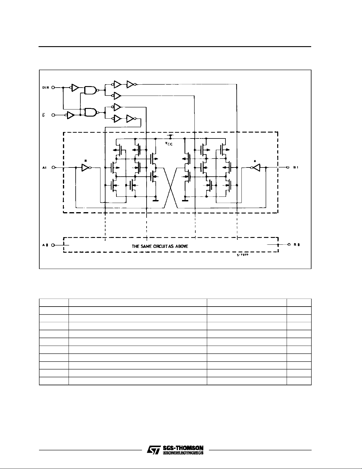
LOGIC DIAGRAM (HCT640)
M54/M74HCT245/640/643
NOTE:IN CASE OF HCT245OR HCT643,INPUTINVERTERSMARKED* AT A BUSAND B BUS AREELIMINATEDRESPECTIVELY
ABSOLU TE M AXIMU M R AT ING S
Symbol Parameter Value Unit
V
CC
V
V
O
I
IK
I
OK
I
O
I
or I
CC
P
D
T
stg
T
AbsoluteMaximumRatingsarethose values beyondwhichdamage tothedevicemayoccur. Functional operationunder these conditionisnotimplied.
(*)500 mW: ≅ 65oC derateto300 mWby 10mW/oC: 65oCto85oC
Supply Voltage -0.5 to +7 V
DC Input Voltage -0.5 to VCC+ 0.5 V
I
DC Output Voltage -0.5 to VCC+ 0.5 V
DC Input Diode Current ± 20 mA
DC Output Diode Current ± 20 mA
DC Output Source Sink Current Per Output Pin ± 35 mA
DC VCCor Ground Current ± 70 mA
GND
Power Dissipation 500 (*) mW
Storage Temperature -65 to +150
Lead Temperature (10sec) 300
L
o
C
o
C
3/11
Page 4
M54/M74HCT245/640/643
RECO MM ENDED OPERAT IN G CO NDITI ONS
Symbol Parameter Value Unit
V
V
V
T
t
r,tf
DC SPECIFICATIONS
Symbol Parameter
V
V
V
OH
V
OL
I
I
OZ
I
CC
∆I
Supply Voltage 4.5 to 5.5 V
CC
Input Voltage 0 to V
I
Output Voltage 0 to V
O
Operating Temperature: M54HC Series
op
M74HC Series
CC
CC
-55 to +125
-40 to +85
Input Rise and Fall Time (VCC= 4.5 to 5.5V) 0 to 500 ns
Test Conditions Value
T
High Level Input
IH
Voltage
V
(V)
4.5
=25oC
CC
A
54HC and 74HC
Min. Typ. Max. Min. Max. Min. Max.
2.0 2.0 2.0 V
to
-40 to 85oC
74HC
-55 to 125oC
5.5
Low Level Input
IL
Voltage
4.5
to
0.8 0.8 0.8 V
5.5
High Level
Output Voltage
Low Level Output
Voltage
Input Leakage
I
Current
3 State Output
VI=
IO=-20 µA 4.4 4.5 4.4 4.4
V
IH
4.5
or
I
=-6.0 mA 4.18 4.31 4.13 4.10
O
V
IL
VI=
IO=20µA 0.0 0.1 0.1 0.1
V
IH
4.5
or
I
= 6.0 mA 0.17 0.26 0.33 0.4
O
V
IL
VI=VCCor GND ±0.1 ±1 ±1 µA
5.5
5.5 VI=VCCor GND ±0.5 ±5.0 ±10 µA
Off State Current
Quiescent Supply
5.5 VI=VCCor GND 4 40 80 µA
Current
Additional worst
CC
case supply
current
5.5 Per Input pin
VI= 0.5V or
V
= 2.4V
I
2.0 2.9 3.0 mA
Other Inputs at
VCCor GND
IO=0
54HC
V
V
o
C
o
C
Unit
V
V
4/11
Page 5

M54/M74HCT245/640/643
AC ELECTRICAL CHARACTERISTICS (CL=50pF,Inputtr=tf=6ns)
Test Conditions Value
T
=25oC
Symbol Parameter
C
t
TLH
t
THL
t
PLH
t
PHL
t
PZL
t
PZH
t
PLZ
t
PHZ
C
I/OUT
Output Transition
Time
Propagation
Delay Time
Output Enable
Time
Output Disable
Time
Input Capacitance DIR, G 5 10 10 10 pF
IN
Output
V
C
CC
(V)
L
(pF)
4.5 50 7 12 15 18 ns
4.5 50 13 22 28 33 ns
4.5 150 18 30 38 45 ns
4.5 50 RL=1KΩ 19 30 38 45 ns
4.5 150 R
=1KΩ 24 38 48 57 ns
L
4.5 50 RL=1KΩ 17 30 38 45
An, Bn 13
A
54HC and 74HC
Min. Typ. Max. Min. Max. Min. Max.
Capacitance
C
(*) Power Dissipation
PD
Capacitance
(*) CPDisdefined as the value ofthe IC’sinternal equivalent capacitance whichis calculated fromthe operatingcurrent consumption without load.
(Referto Test Circuit). Average opertingcurrent can beobtained by the followingequation. ICC(opr) = CPD•VCC•fIN+ICC/8(per circuit)
HCT245
HCT640/643
41
39
-40 to 85oC
74HC
-55 to 125oC
54HC
Unit
ns
pF
pF
SWITCHING CHARACTERISTICS TEST WAVEFORM
5/11
Page 6

M54/M74HCT245/640/643
TEST CIRCUIT ICC(Opr.) CPDCALCULATION
CPDis to be calculated with the following
formula by using the measured value of I
(Opr.)in thetest circuit opposite.
CPD=
In determining the value of CPD, a relatively
high frequency of 1MHzwas applied to fIN,in
orther to eliminate any error caused by the
quiescent supply current.
I
(
Opr
CC
fINxV
CC
.)
CC
6/11
Page 7

M54/M74HCT245/640/643
Plastic DIP20 (0.25) MECHANICAL DATA
DIM.
MIN. TYP. MAX. MIN. TYP. MAX.
a1 0.254 0.010
B 1.39 1.65 0.055 0.065
b 0.45 0.018
b1 0.25 0.010
D 25.4 1.000
E 8.5 0.335
e 2.54 0.100
e3 22.86 0.900
F 7.1 0.280
I 3.93 0.155
L 3.3 0.130
Z 1.34 0.053
mm inch
P001J
7/11
Page 8

M54/M74HCT245/640/643
Ceramic DIP20 MECHANICAL DATA
DIM.
MIN. TYP. MAX. MIN. TYP. MAX.
A 25 0.984
B 7.8 0.307
D 3.3 0.130
E 0.5 1.78 0.020 0.070
e3 22.86 0.900
F 2.29 2.79 0.090 0.110
G 0.4 0.55 0.016 0.022
I 1.27 1.52 0.050 0.060
L 0.22 0.31 0.009 0.012
M 0.51 1.27 0.020 0.050
N1 4° (min.), 15° (max.)
P 7.9 8.13 0.311 0.320
Q 5.71 0.225
mm inch
8/11
P057H
Page 9

SO20 MECHANICAL DATA
M54/M74HCT245/640/643
DIM.
MIN. TYP. MAX. MIN. TYP. MAX.
A 2.65 0.104
a1 0.10 0.20 0.004 0.007
a2 2.45 0.096
b 0.35 0.49 0.013 0.019
b1 0.23 0.32 0.009 0.012
C 0.50 0.020
c1 45° (typ.)
D 12.60 13.00 0.496 0.512
E 10.00 10.65 0.393 0.419
e 1.27 0.050
e3 11.43 0.450
F 7.40 7.60 0.291 0.299
L 0.50 1.27 0.19 0.050
M 0.75 0.029
S8°(max.)
mm inch
P013L
9/11
Page 10

M54/M74HCT245/640/643
PLCC20 MECHANICAL DATA
DIM.
MIN. TYP. MAX. MIN. TYP. MAX.
A 9.78 10.03 0.385 0.395
B 8.89 9.04 0.350 0.356
D 4.2 4.57 0.165 0.180
d1 2.54 0.100
d2 0.56 0.022
E 7.37 8.38 0.290 0.330
e 1.27 0.050
e3 5.08 0.200
F 0.38 0.015
G 0.101 0.004
M 1.27 0.050
M1 1.14 0.045
mm inch
10/11
P027A
Page 11

M54/M74HCT245/640/643
Information furnishedis believed to be accurate and reliable. However, SGS-THOMSON Microelectronicsassumes no responsability for the
consequences of useof suchinformation nor for any infringement of patents or other rights of third parties which may results from its use. No
license is granted byimplication or otherwiseunder any patentor patentrights ofSGS-THOMSON Microelectronics.Specificationsmentioned
in thispublication are subjectto changewithout notice. This publication supersedes andreplaces all information previouslysupplied.
SGS-THOMSON Microelectronicsproducts are not authorized foruse ascritical componentsinlife supportdevices or systems without express
written approval of SGS-THOMSON Microelectonics.
1994SGS-THOMSON Microelectronics- All Rights Reserved
Australia -Brazil - France - Germany - Hong Kong - Italy -Japan - Korea - Malaysia - Malta -Morocco - The Netherlands-
Singapore -Spain - Sweden- Switzerland - Taiwan - Thailand- UnitedKingdom - U.S.A
SGS-THOMSON Microelectronics GROUP OFCOMPANIES
11/11
 Loading...