

Page 1

OCTAL D-TYPE FLIP FLOP WITH 3 STATE OUTPUT
HCT564 INVERTING - HCT574 NONINVERTING
.HIGH SPEED
f
= 62 MHz (TYP.) AT VCC=5V
MAX
.LOWPOWER DISSIPATION
ICC=4µA(MAX.) AT TA=25°C
.COMPATIBLE WITH TTL OUTPUTS
VIH= 2V (MIN.) VIL= 0.8V (MAX)
.OUTPUT DRIVE CAPABILITY
15 LSTTL LOADS
.SYMMETRICALOUTPUT IMPEDANCE
IOL=IOH= 6 mA (MIN.)
.BALANCEDPROPAGATION DELAYS
t
PLH=tPHL
.PIN ANDFUNCTION COMPATIBLE
WITH 54/74LS564/574
DESCRIPTION
The M54/74HCT564 and M54HCT574 are high
speed CMOS OCTALD-TYPEFLIPFLOPWITH3STATEOUTPUTSfabricatedinsilicongateC2MOS
technology. They have the same high speed performance of LSTTL combined with true CMOSlow
power comsuption.These 8-bit D-type flip-flops are
controlled byaclockinput(CK)and anouputenable
input(OE).Onthepositivetransitionoftheclock,the
Qoutputswillbesettothelogicstatethatweresetup
at the D inputs (HCT574) or their complements
(HCT564).
While the OEinput is low, the eight outputs will be
in a normal logic state (high or low logic level), and
while highlevel, theoutputs willbe ina high impedancestate.The outputcontrol does notaffectthein-
M54/74HCT564
M54/74HCT574
B1R
(PlasticPackage)
M1R
(MicroPackage)
ORDER CODES :
M54HCTX XX F1R M74HCTX XXM1 R
M7 4HCTXXXB1 R M7 4HCTXXXC1R
ternaloperationofflip-flops. Thatis, theolddatacan
be retained or the new data can be entered even
while the outputs are off. The application engineer
has achoice of combinationof inverting and non-inverting outputs. The 3-state output configuration
and the wide choice of outline make bus-organized
systemssimple.Allinputs areequipped withprotection circuits against static discharge and transient
excessvoltage. Thisintegrated circuithas inputand
output characteristics that are fully compatiblewith
54/74 LSTTL logic families. M54/74HCT devices
are designed to directly interface HSC2MOS systems with TTL and NMOS components. They are
also plugin replacements for LSTTL devices giving
a reduction ofpower consumption.
F1R
(CeramicPackage)
C1R
(Chip Carrier)
PIN CONNECTION (top view)
HCT564 HCT574 HCT564 HCT574
September 1993
1/13
Page 2
M54/M74HCT564/574
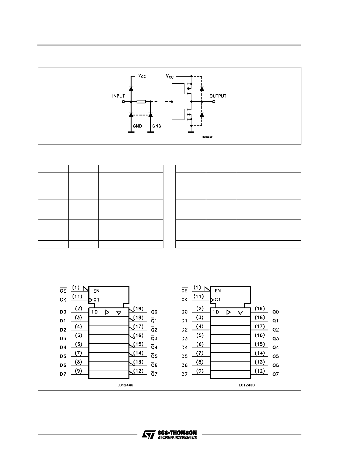
INPUT AND OUTPUT EQUIVALENT CIRCUIT
PIN DESCRIPTION (HCT564)
PIN No SYMBOL NAME AND FUNCTION
1 OE 3 State output Enable
Input (Active LOW)
2, 3, 4, 5,
6, 7, 8, 9
12, 13, 14,
15, 16, 17,
18, 19
11 CLOCK Clock Input (LOW to
10 GND Ground (0V)
20 V
D0 to D7 Data Inputs
Q0 to Q7 3 State outputs
HIGH, edge triggered)
CC
Positive Supply Voltage
IEC LOGIC SYMBOLS
PIN DESCRIPTIO N (HC T574)
PIN No SYMBOL NAME AND FUNCTION
1 OE 3 State output Enable
Input (Active LOW)
2, 3, 4, 5,
6, 7, 8, 9
12, 13, 14,
15, 16, 17,
18, 19
11 CLOCK Clock Input (LOW to
10 GND Ground (0V)
20 V
D0 to D7 Data Inputs
Q0 to Q7 3 State outputs
HIGH, edge triggered)
CC
HCT574HCT564
Positive Supply Voltage
2/13
Page 3
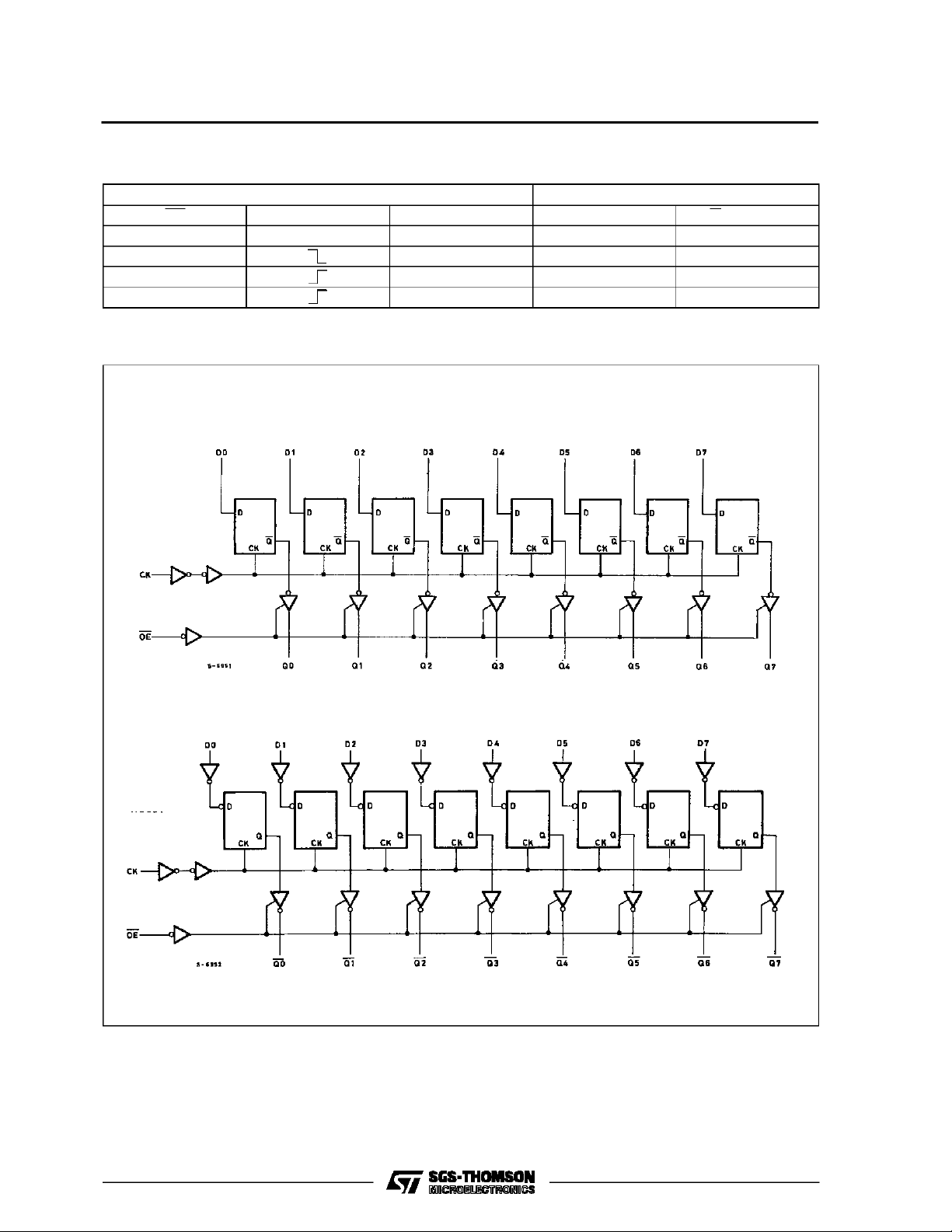
TRUTH TABLE
OE CK D Q (HCT574) Q (HCT564)
HXXZZ
L X NO CHANGE NO CHANGE
LLLH
LHHL
LOGIC DIAGRAMS
HCT574
M54/M74HCT564/574
INPUTS OUTPUTS
HCT564
3/13
Page 4

M54/M74HCT564/574
ABSOLU TE MAXIMU M R AT I NG S
Symbol Parameter Value Unit
V
CC
V
V
O
I
IK
I
OK
I
O
I
or I
CC
P
D
T
stg
T
AbsoluteMaximumRatingsarethosevaluesbeyondwhichdamage tothedevicemayoccur.Functionaloperationunder theseconditionisnotimplied.
(*)500 mW:≅ 65oC derateto 300 mW by 10mW/oC: 65oCto85oC
RECO MM ENDED O PERAT IN G C O NDI TIONS
Symbol Parameter Value Unit
V
CC
V
I
V
O
T
op
t
r,tf
Supply Voltage -0.5 to +7 V
DC Input Voltage -0.5 to VCC+ 0.5 V
I
DC Output Voltage -0.5 to VCC+ 0.5 V
DC Input Diode Current ± 20 mA
DC Output Diode Current ± 20 mA
DC Output Source Sink Current Per Output Pin ± 35 mA
DC VCCor Ground Current ± 70 mA
GND
Power Dissipation 500 (*) mW
Storage Temperature -65 to +150
Lead Temperature (10 sec) 300
L
Supply Voltage 4.5 to 5.5 V
Input Voltage 0 to V
Output Voltage 0 to V
Operating Temperature: M54HC Series
M74HC Series
CC
CC
-55 to +125
-40 to +85
Input Rise and Fall Time (VCC= 4.5 to 5.5V) 0 to 500 ns
o
C
o
C
V
V
o
C
o
C
4/13
Page 5

DC SPECIFICATIO NS
Symbol Parameter
V
V
V
V
I
∆I
High Level Input
IH
Voltage
Low Level Input
IL
Voltage
High Level
OH
Output Voltage
Low Level Output
OL
Voltage
Input Leakage
I
I
Current
Quiescent Supply
CC
Current
Additional worst
CC
case supply
current
M54/M74HCT564/574
Test Conditions Value
T
=25oC
V
(V)
4.5
CC
A
54HC and 74HC
Min. Typ. Max. Min. Max. Min. Max.
2.0 2.0 2.0 V
to
5.5
4.5
to
5.5
VI=
IO=-20 µA 4.4 4.5 4.4 4.4
V
IH
4.5
or
I
=-6.0 mA 4.18 4.31 4.13 4.10
O
V
IL
VI=
IO=20µA 0.0 0.1 0.1 0.1
V
IH
4.5
or
I
= 6.0 mA 0.17 0.26 0.33 0.4
O
V
IL
VI=VCCor GND ±0.1 ±1 ±1 µA
5.5
5.5 VI=VCCor GND 4 40 80 µA
5.5 Per Input pin
VI= 0.5V or
V
= 2.4V
I
Other Inputs at
VCCor GND
IO=0
-40 to 85oC
74HC
-55 to 125oC
54HC
Unit
0.8 0.8 0.8 V
2.0 2.9 3.0 mA
V
V
5/13
Page 6

M54/M74HCT564/574
AC ELECTRICAL CHARACTERISTICS (CL=50pF,Inputtr=tf=6ns)
Test Conditions Value
T
=25oC
Symbol Parameter
t
TLH
t
THL
t
PLH
t
PHL
t
PZL
t
PZH
t
PLZ
t
PHZ
f
MAX
Output Transition
Time
Propagation
Delay Time
3 State Output
Enable Time
3 State Output
Disable Time
Maximum CLock
V
C
CC
(V)
L
(pF)
4.5 50 7 12 15 18
4.5 50 20 30 38 45
4.5 150 24 36 45 54
4.5 50 RL=1KΩ 19 30 38 45
4.5 150 R
=1KΩ 23 36 45 54
L
4.5 50 RL=1KΩ 19 30 38 45
4.5 50 31 50 25 21
A
54HC and 74HC
Min. Typ. Max. Min. Max. Min. Max.
Frequency
t
W(L)
t
W(H)
t
s
Minimum Pulse
Width (CLOCK)
Minimum Set-up
4.5 50 8 15 19 22
4.5 50 7 15 19 22
Time
t
h
Minimum Hold
4.5 50 0 0 0
Time
C
C
Input Capacitance 5 10 10 10 pF
IN
OUT
Out put
10
Capacitance
C
(*) Power Dissipation
PD
Capacitance
(*) CPDisdefined asthevalueof the IC’sinternal equivalentcapacitance whichis calculatedfromthe operating current consumption without load.
(Refer to Test Circuit). Averageopertingcurrent can be obtainedby thefollowingequation. ICC(opr) =CPD•VCC•fIN+ICC(perFlip-Flop)
HCT564
HCT574
67
63
-40 to 85oC
74HC
-55 to 125oC
54HC
Unit
ns
ns
ns
ns
ns
ns
ns
ns
pF
pF
6/13
Page 7

SWITCHING CHARACTERISTICS TEST WAVEFORM
CLOCK DUTY : 50%
f
MAX
M54/M74HCT564/574
1
=
T
CK
EACHFLIP-FLOPSHALL BE SET HIGHWHEN SWITCHIS CONNECTED TO GND LINE AND IT SHALL BE SETLOW WHEN
SWITCHIS CONNECTED TO VCCLINE.
7/13
Page 8

M54/M74HCT564/574
TEST CIRCUIT ICC(Opr.)
INPUTWAVEFORM ISTHE SAME AS THATIN CASE OFSWITCHINGCHARACTERISTICSTEST.
8/13
Page 9

M54/M74HCT564/574
Plastic DIP20 (0.25) MECHANICAL DATA
DIM.
MIN. TYP. MAX. MIN. TYP. MAX.
a1 0.254 0.010
B 1.39 1.65 0.055 0.065
b 0.45 0.018
b1 0.25 0.010
D 25.4 1.000
E 8.5 0.335
e 2.54 0.100
e3 22.86 0.900
F 7.1 0.280
I 3.93 0.155
L 3.3 0.130
Z 1.34 0.053
mm inch
P001J
9/13
Page 10

M54/M74HCT564/574
Ceramic DIP20 MECHANICAL DATA
DIM.
MIN. TYP. MAX. MIN. TYP. MAX.
A 25 0.984
B 7.8 0.307
D 3.3 0.130
E 0.5 1.78 0.020 0.070
e3 22.86 0.900
F 2.29 2.79 0.090 0.110
G 0.4 0.55 0.016 0.022
I 1.27 1.52 0.050 0.060
L 0.22 0.31 0.009 0.012
M 0.51 1.27 0.020 0.050
N1 4° (min.), 15° (max.)
P 7.9 8.13 0.311 0.320
Q 5.71 0.225
mm inch
10/13
P057H
Page 11

SO20 MECHANICAL DATA
M54/M74HCT564/574
DIM.
MIN. TYP. MAX. MIN. TYP. MAX.
A 2.65 0.104
a1 0.10 0.20 0.004 0.007
a2 2.45 0.096
b 0.35 0.49 0.013 0.019
b1 0.23 0.32 0.009 0.012
C 0.50 0.020
c1 45° (typ.)
D 12.60 13.00 0.496 0.512
E 10.00 10.65 0.393 0.419
e 1.27 0.050
e3 11.43 0.450
F 7.40 7.60 0.291 0.299
L 0.50 1.27 0.19 0.050
M 0.75 0.029
S8°(max.)
mm inch
P013L
11/13
Page 12

M54/M74HCT564/574
PLCC20 MECHANICAL DATA
DIM.
MIN. TYP. MAX. MIN. TYP. MAX.
A 9.78 10.03 0.385 0.395
B 8.89 9.04 0.350 0.356
D 4.2 4.57 0.165 0.180
d1 2.54 0.100
d2 0.56 0.022
E 7.37 8.38 0.290 0.330
e 1.27 0.050
e3 5.08 0.200
F 0.38 0.015
G 0.101 0.004
M 1.27 0.050
M1 1.14 0.045
mm inch
12/13
P027A
Page 13

M54/M74HCT564/574
Information furnishedis believed to be accurate and reliable.However, SGS-THOMSON Microelectronicsassumes no responsability for the
consequences of useof suchinformation nor forany infringementof patents or other rights of third partieswhich mayresults from its use. No
license is granted byimplication orotherwise under any patentor patent rights ofSGS-THOMSON Microelectronics.Specificationsmentioned
in this publication are subject to changewithout notice.This publication supersedes and replacesall informationpreviously supplied.
SGS-THOMSON Microelectronicsproducts are not authorized foruse ascritical componentsinlife supportdevices orsystemswithoutexpress
written approval of SGS-THOMSON Microelectonics.
1994 SGS-THOMSON Microelectronics- All RightsReserved
Australia -Brazil - France - Germany - Hong Kong - Italy - Japan- Korea - Malaysia - Malta - Morocco - The Netherlands -
Singapore -Spain - Sweden- Switzerland -Taiwan - Thailand- UnitedKingdom - U.S.A
SGS-THOMSON Microelectronics GROUP OFCOMPANIES
13/13
 Loading...