

Page 1
M54/74HCT563
M54/74HCT573
October1993
HCT563 INVERTING - HCT573 NONINVERTING
OCTAL D-TYPE LATCH WITH 3 STATE OUTPUT
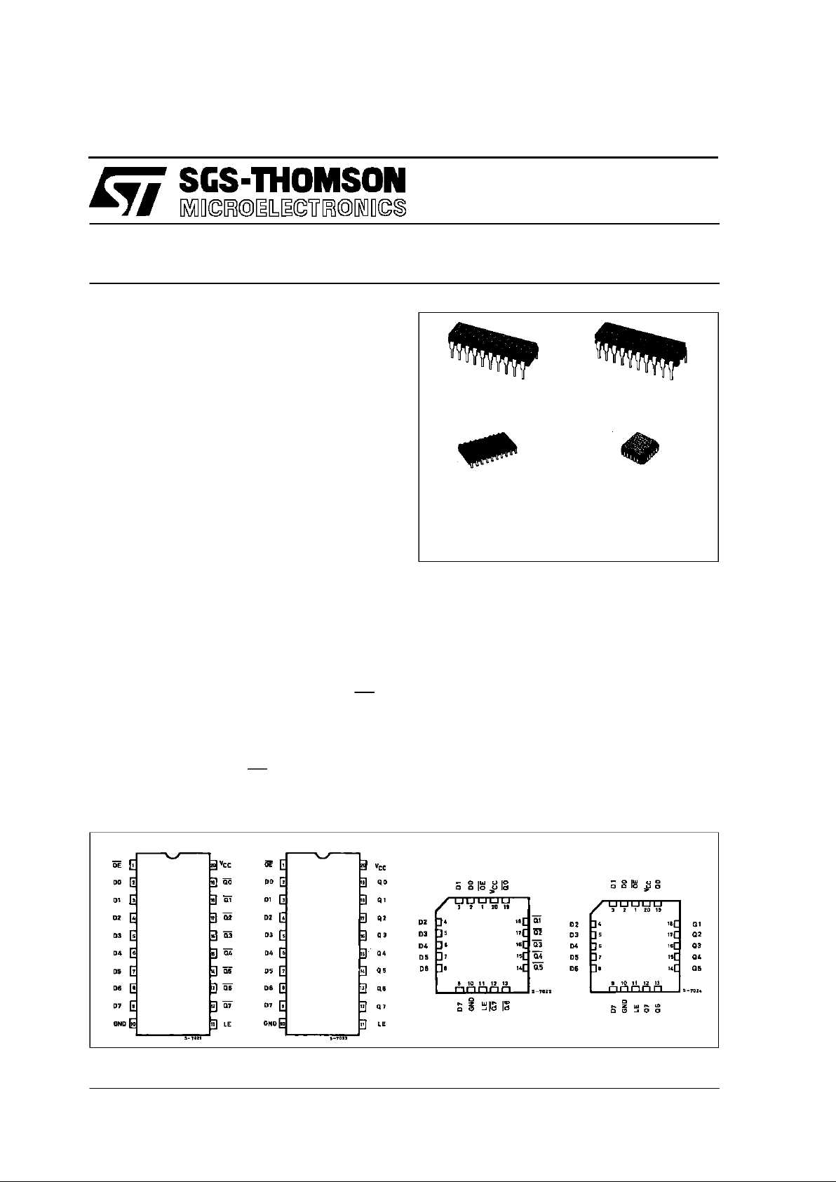
B1R
(PlasticPackage)
ORDER CODES :
M5 4HCT XXXF1R M74H CT X XXM1R
M74HCTX XX B1R M74HCTXXXC 1R
F1R
(CeramicPackage)
M1R
(MicroPackage)
C1R
(Chip Carrier)
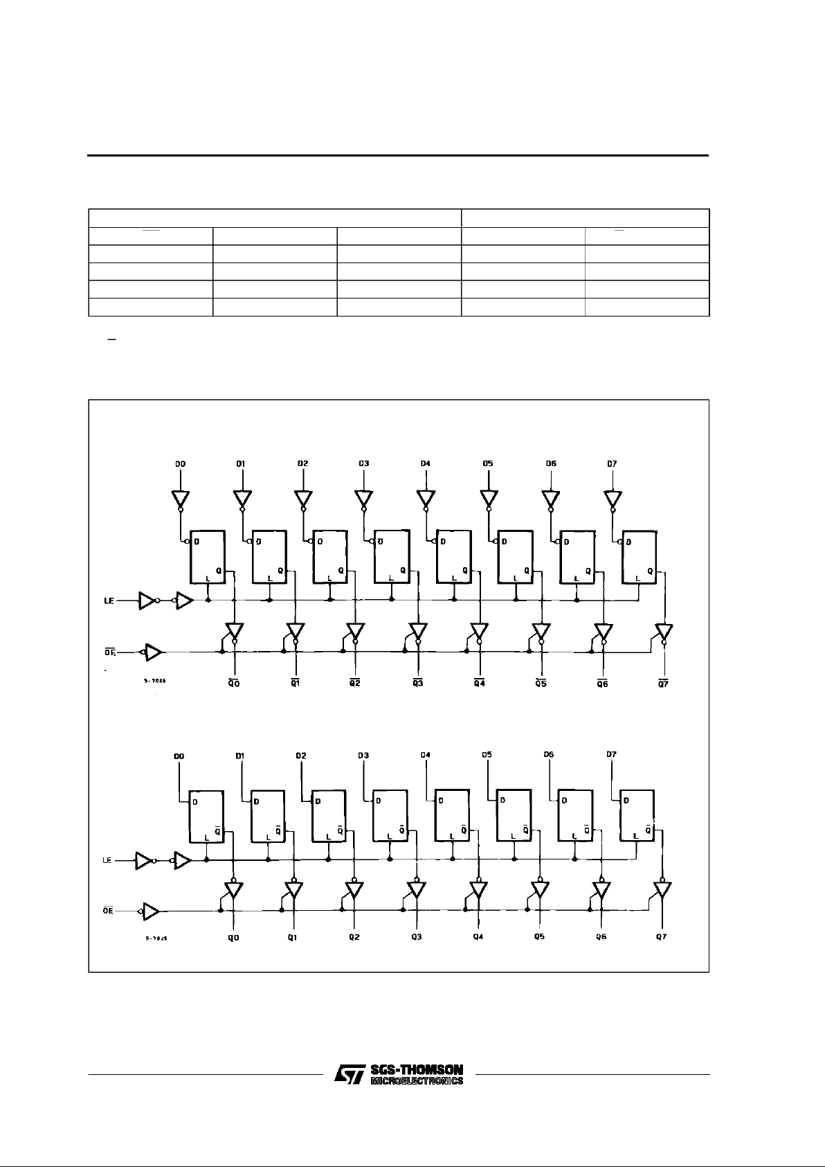
PIN CONNECTION (top view)
.HIGH SPEED
tPD= 18 ns(TYP.) AT VCC=5V
.LOWPOWER DISSIPATION
ICC=4µA(MAX.) AT TA=25°C
.COMPATIBLE WITHTTL OUTPUTS
VIH= 2V (MIN.) VIL= 0.8V (MAX.)
.OUTPUTDRIVE CAPABILITY
15 LSTTL LOADS
.SYMMETRICAL OUTPUT IMPEDANCE
IOL=IOH= 6 mA (MIN.)
.BALANCEDPROPAGATIONDELAYS
t
PLH=tPHL
.PIN ANDFUNCTION COMPATIBLE
WITH 54/74LS563/573
DESCRIPTION
The M54/74HCT563 and M54HCT573 are high
speed CMOS OCTAL LATCH WITH 3-STATE
OUTPUTS fabricated with silicon gate C2MOS
technology.
These ICs achive the high speed operation similar
to equivalent LSTTL while maintaining the CMOS
low power dissipation.
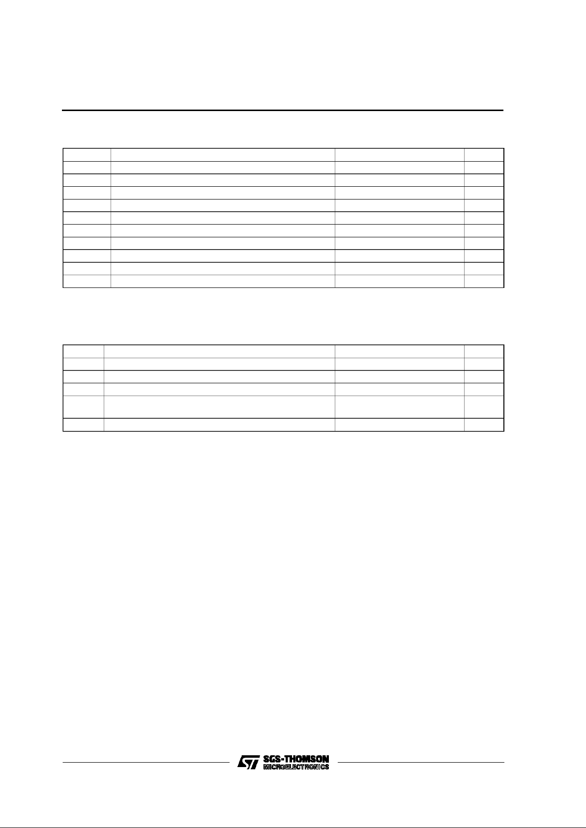
These8 bitD-Typelatchesare controlled by a latch
enable input (LE) and aoutput enable input (OE).
While the LE input is held at a high level, the Q
outputs will follow the data input precisely or
inversely. When the LE is taken low, the Q outputs
willbe latchedprecisely orinversely atthelogiclevel
of D input data. While the OE input is at low level,
the eightoutputs will be inanormal logicstate(high
or lowlogiclevel) andwhilehighlevel the outpts will
be in a high impedance state.
The application designer has a choise of
combination of invertingand non invertingoutputs.
This integrated circuit has input and output
characteristics that are fully compatible with 54/74
LSTTL logic families. M54/74HCT devices are
designed to directly interface HSC2MOS systems
with TTL and NMOS components. They are also
plug in replacements for LSTTL devices giving a
reduction of powerconsumption.
All inputs are equipped with protection circuits
against discharge and transient excessvoltage.
HCT563 HCT573 HCT563 HCT573
1/13
Page 2

INPUT AND OUTPUT EQUIVALENT CIRCUIT
PIN DESCRIPTION (HCT 563)
PIN No SYMBOL NAME AND FUNCTION
1 OE 3 State output Enable
Input (Active LOW)
2, 3, 4, 5,
6, 7, 8, 9
D0 to D7 Data Inputs
12, 13, 14,
15, 16, 17,
18, 19
Q0 to Q7 3 State Latch Outputs
11 LE Latch Enable Input
10 GND Ground (0V)
20 V
CC
Positive Supply Voltage
PIN DESCRIPTIO N (HC T573)
PIN No SYMBOL NAME AND FUNCTION
1 OE 3 State output Enable
Input (Active LOW)
2, 3, 4, 5,
6, 7, 8, 9
D0 to D7 Data Inputs
12, 13, 14,
15, 16, 17,
18, 19
Q0 to Q7 3 State Latch Outputs
11 LE Latch Enable Input
10 GND Ground (0V)
20 V
CC
Positive Supply Voltage
IEC LOGIC SYMBOLS
HCT563 HCT573
M54/M74HCT563/573
2/13
Page 3
TRUTH TABLE
INPUTS OUTPUTS
OE LE D Q (HCT573) Q (HCT563)
HXXZZ
L L X NO CHANGE * NO CHANGE *
LHLLH
LHHHL
X: DON’TCARE
Z: HIGHIMPEDANCE
*: Q/QOUTPUTSARE LATCHEDAT THE TIME WHENTHE LE INPUTIS TAKENLOW LOGIC LEVEL.
LOGIC DIAGRAMS
HCT563
HCT573
M54/M74HCT563/573
3/13
Page 4
ABSOLU TE MAXIMU M R AT I NG S
Symbol Parameter Value Unit
V
CC
Supply Voltage -0.5 to +7 V
V
I
DC Input Voltage -0.5 to VCC+ 0.5 V
V
O
DC Output Voltage -0.5 to VCC+ 0.5 V
I
IK
DC Input Diode Current ± 20 mA
I
OK
DC Output Diode Current ± 20 mA
I
O
DC Output Source Sink Current Per Output Pin ± 35 mA
I
CC
or I
GND
DC VCCor Ground Current ± 70 mA
P
D
Power Dissipation 500 (*) mW
T
stg
Storage Temperature -65 to +150
o
C
T
L
Lead Temperature (10 sec) 300
o
C
AbsoluteMaximumRatingsarethosevaluesbeyondwhichdamage to thedevicemayoccur.Functionaloperationunder theseconditionisnotimplied.
(*)500 mW:≅ 65oC derate to 300 mW by 10mW/oC: 65oCto85oC
RECO MM ENDED O PERAT IN G CONDITIONS
Symbol Parameter Value Unit
V
CC
Supply Voltage 4.5 to 5.5 V
V
I
Input Voltage 0 to V
CC
V
V
O
Output Voltage 0 to V
CC
V
T
op
Operating Temperature: M54HC Series
M74HC Series
-55 to +125
-40 to +85
o
C
o
C
t
r,tf
Input Rise and Fall Time (VCC= 4.5 to 5.5V) 0 to 500 ns
M54/M74HCT563/573
4/13
Page 5

DC SPECIFICATIO NS
Symbol Parameter
Test Conditions Value
Unit
V
CC
(V)
T
A
=25oC
54HC and 74HC
-40 to 85oC
74HC
-55 to 125oC
54HC
Min. Typ. Max. Min. Max. Min. Max.
V
IH
High Level Input
Voltage
4.5
to
5.5
2.0 2.0 2.0 V
V
IL
Low Level Input
Voltage
4.5
to
5.5
0.8 0.8 0.8 V
V
OH
High Level
Output Voltage
4.5
VI=
V
IH
or
V
IL
IO=-20 µA 4.4 4.5 4.4 4.4
V
I
O
=-6.0 mA 4.18 4.31 4.13 4.10
V
OL
Low Level Output
Voltage
4.5
VI=
V
IH
or
V
IL
IO=20µA 0.0 0.1 0.1 0.1
V
I
O
= 6.0 mA 0.17 0.26 0.33 0.4
I
I
Input Leakage
Current
5.5
VI=VCCor GND ±0.1 ±1 ±1 µA
I
OZ
3 State Output
Off State Current
5.5 VI=VIHor V
IL
VO=VCCor GND
±0.5 ±5.0 ±10 µA
I
CC
Quiescent Supply
Current
5.5 VI=VCCor GND 4 40 80 µA
∆I
CC
Additional worst
case supply
current
5.5 Per Input pin
VI= 0.5V or
VI= 2.4V
Other Inputs at
V
CC
or GND
2.0 2.9 3.0 mA
M54/M74HCT563/573
5/13
Page 6

AC ELECTRICAL CHARACTERISTICS (CL=50pF,Inputtr=tf=6ns)
Symbol Parameter
Test Conditions Value
Unit
V
CC
(V)
C
L
(pF)
T
A
=25oC
54HC and 74HC
-40 to 85oC
74HC
-55 to 125oC
54HC
Min. Typ. Max. Min. Max. Min. Max.
t
TLH
t
THL
Output Transition
Time
4.5 50 7 12 15 18 ns
t
PLH
t
PHL
Propagation
Delay Time
(LE - Q, Q)
4.5 50 21 33 41 50 ns
4.5 150 25 39 49 59 ns
t
PLH
t
PHL
Propagation
Delay Time
(D - Q, Q)
4.5 50 19 30 38 45 ns
4.5 150 23 36 45 54 ns
t
PZL
t
PZH
3 State Output
Enable Time
4.5 50 RL=1KΩ 19 30 38 45 ns
4.5 150 R
L
=1KΩ 23 36 45 54 ns
t
PZL
t
PZH
3 State Output
Disable Time
4.5 50 RL=1KΩ 18 25 31 38 ns
t
W(L)
t
W(H)
Minimum Pulse
Width (LE)
4.5 50 7 15 19 22 ns
t
s
Minimum Set-up
Time
4.5 50 4 10 13 15 ns
t
h
Minimum Hold
Time
4.5 50 5 5 5 ns
C
IN
Input Capacitance 5 10 10 10 pF
C
OUT
Output
Capacitance
10
pF
C
PD
(*) Power Dissipation
Capacitance
51
pF
(*) CPDisdefinedas the value of the IC’s internalequivalent capacitance which is calculated fromthe operating currentconsumption withoutload.
(Refer to TestCircuit).Averageoperting current can beobtained by thefollowing equation. ICC(opr) = CPD•VCC•fIN+ICC/8(per Flip-Flop)
M54/M74HCT563/573
6/13
Page 7

SWITCHING CHARACTERISTICS TEST WAVEFORM
t
PLZ,tPZL
The 1KΩ load resistors should be connected between
outputs and VCCline and the 50pF load capacitors
should be connected between outputsand GND line.
All inputs except OE input should be connected to V
CC
line or GND line such that outputs will be in low logic
level while OE input is held low.
t
PHZ,tPZH
The 1KΩ load resistors and the 50pF load capacitors
should be connected between each output and GND
line.
All inputs except OE input should be connected to V
CC
or GND line such that output will be in high logic level
while OE input is held low.
t
PLH,tPHL
(D - Q) t
PLH,tPHL
(LE - Q), ts,th,t
w
M54/M74HCT563/573
7/13
Page 8

TEST CIRCUIT ICC(Opr.)
INPUTWAVEFORM ISTHE SAMEAS THAT IN CASE OF SWITCHINGCHARACTERISTICSTEST.
M54/M74HCT563/573
8/13
Page 9

Plastic DIP20 (0.25) MECHANICAL DATA
DIM.
mm inch
MIN. TYP. MAX. MIN. TYP. MAX.
a1 0.254 0.010
B 1.39 1.65 0.055 0.065
b 0.45 0.018
b1 0.25 0.010
D 25.4 1.000
E 8.5 0.335
e 2.54 0.100
e3 22.86 0.900
F 7.1 0.280
I 3.93 0.155
L 3.3 0.130
Z 1.34 0.053
P001J
M54/M74HCT563/573
9/13
Page 10

Ceramic DIP20 MECHANICAL DATA
DIM.
mm inch
MIN. TYP. MAX. MIN. TYP. MAX.
A 25 0.984
B 7.8 0.307
D 3.3 0.130
E 0.5 1.78 0.020 0.070
e3 22.86 0.900
F 2.29 2.79 0.090 0.110
G 0.4 0.55 0.016 0.022
I 1.27 1.52 0.050 0.060
L 0.22 0.31 0.009 0.012
M 0.51 1.27 0.020 0.050
N1 4° (min.), 15° (max.)
P 7.9 8.13 0.311 0.320
Q 5.71 0.225
P057H
M54/M74HCT563/573
10/13
Page 11

SO20 MECHANICAL DATA
DIM.
mm inch
MIN. TYP. MAX. MIN. TYP. MAX.
A 2.65 0.104
a1 0.10 0.20 0.004 0.007
a2 2.45 0.096
b 0.35 0.49 0.013 0.019
b1 0.23 0.32 0.009 0.012
C 0.50 0.020
c1 45° (typ.)
D 12.60 13.00 0.496 0.512
E 10.00 10.65 0.393 0.419
e 1.27 0.050
e3 11.43 0.450
F 7.40 7.60 0.291 0.299
L 0.50 1.27 0.19 0.050
M 0.75 0.029
S8°(max.)
P013L
M54/M74HCT563/573
11/13
Page 12

PLCC20 MECHANICAL DATA
DIM.
mm inch
MIN. TYP. MAX. MIN. TYP. MAX.
A 9.78 10.03 0.385 0.395
B 8.89 9.04 0.350 0.356
D 4.2 4.57 0.165 0.180
d1 2.54 0.100
d2 0.56 0.022
E 7.37 8.38 0.290 0.330
e 1.27 0.050
e3 5.08 0.200
F 0.38 0.015
G 0.101 0.004
M 1.27 0.050
M1 1.14 0.045
P027A
M54/M74HCT563/573
12/13
Page 13

Information furnished is believed to be accurate and reliable. However, SGS-THOMSON Microelectronicsassumes no responsability for the
consequences of use of such information nor for any infringement of patents or other rights of third partieswhich may results from its use. No
license isgranted byimplication or otherwiseunder any patentor patent rights of SGS-THOMSON Microelectronics. Specificationsmentioned
in this publication are subject to change without notice. This publication supersedes and replaces all information previously supplied.
SGS-THOMSON Microelectronicsproductsare notauthorized foruse ascritical componentsin life support devicesor systems withoutexpress
written approval of SGS-THOMSON Microelectonics.
1994 SGS-THOMSON Microelectronics - All Rights Reserved
SGS-THOMSON Microelectronics GROUP OF COMPANIES
Australia - Brazil - France - Germany - Hong Kong - Italy - Japan - Korea - Malaysia - Malta - Morocco - The Netherlands -
Singapore - Spain - Sweden - Switzerland - Taiwan - Thailand - UnitedKingdom - U.S.A
M54/M74HCT563/573
13/13
 Loading...