

Page 1
OCTAL BUS BU FFER WITH3 STATEOUTPUTS
HCT540: INVERTED - HCT541 NON INVERTED
.HIGH SPEED
tPD= 10 ns(TYP.) at VCC=5V
.LOWPOWER DISSIPATION
ICC=4µA (MAX.) at TA=25oC
.COMPATIBLE WITH TTL OUTPUTS
VIH= 2V (MIN.) VIL= 0.8V (MAX.)
.OUTPUTDRIVE CAPABILITY
15 LSTTL LOADS
.SYMMETRICALOUTPUT IMPEDANCE
|IOH|=IOL=6 mA (MIN)
.BALANCEDPROPAGATIONDELAYS
t
PLH=tPHL
.PIN AND FUNCTION COMPATIBLE
WITH 54/74LS540/541
DESCRIPTION
M54HCT540/541
M74HCT540/541
B1R
(PlasticPackage)
M1R
(MicroPackage)
ORDER CODE S :
M54HC TXXXF1R M74HC TXXXM1R
M74HC TXXXB1R M74HCT XXXC1R
F1R
(CeramicPackage)
C1R
(Chip Carrier)
The M54/74HCT540 and HCT541are high speed
CMOS OCTAL BUS BUFFERS (3-STATE)
fabricated in silicongate C2MOStechnology. They
have the same high speed performance of LSTTL
combined withtrue CMOS lowpower consumption.
The HCT540isaninverting bufferand HCT541 is a
non inverting buffer.
The 3 STATE control gate operates as a two input
AND suchthatifeither G1 andG2 are high,all eight
outputs are in thehigh impedance state. In order to
enhance PC board layout, the HCT540 and
HCT541 offers a pinout having inputs and outputs
on opposite sides of the package. All inputs are
equipped with protection circuits against static
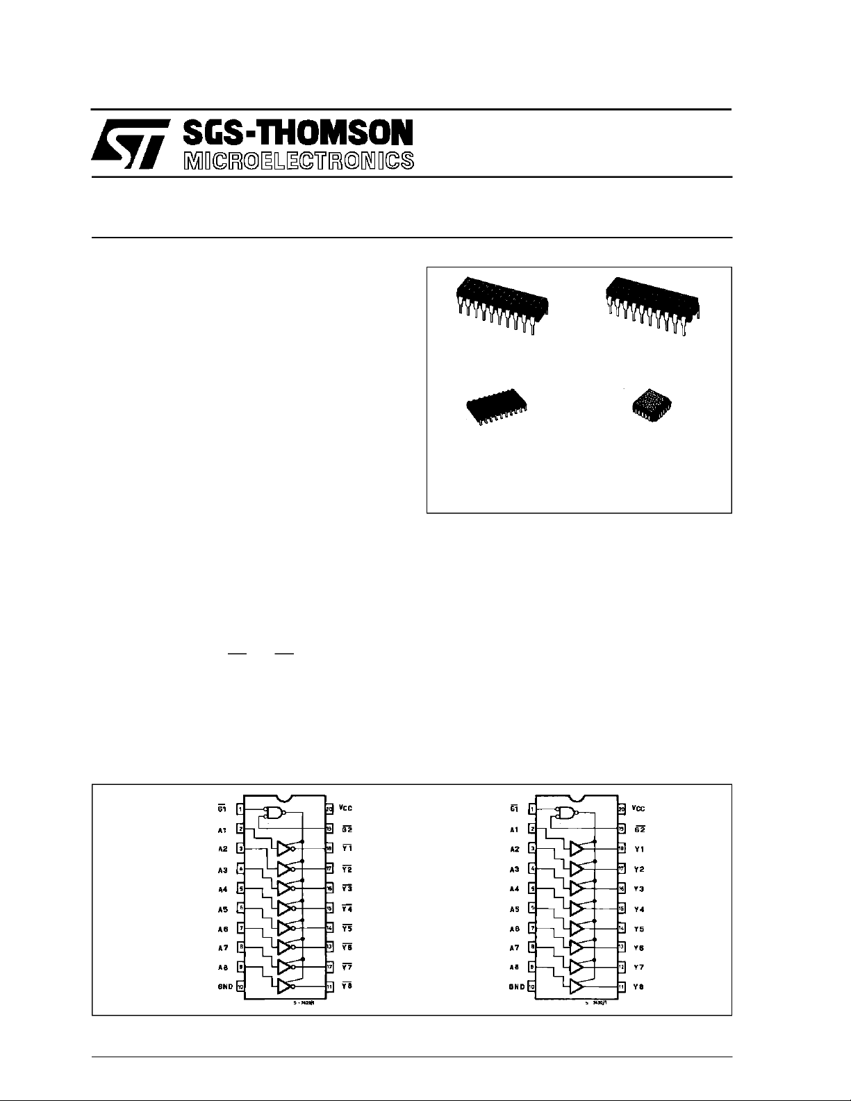
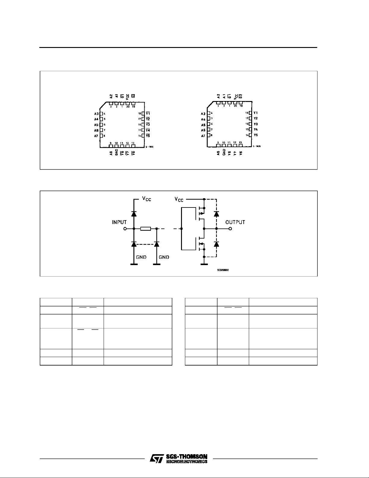
PIN CONNECTION (top view)
discharge and transient excess voltage.
This integrated circuit has input and output
characteristics that are fully compatible with 54/74
LSTTL logic families. M54/74HCT devices are
designed to directly interface HSC2MOS systems
with TTL and NMOS components. They are also
plug in replacements for LSTTL devices giving a
reduction of power consumption.
IT IS PROHIBITEDTO APPLY A SIGNALTO BUS
TERMINAL WHEN IT IS IN OUTPUT MODE.
WHEN A BUS TERMINAL IS FLOATING (HIGH
IMPEDANCE STATE) IT IS REQUESTED TO FIX
THE INPUT LEVEL BY MEANS OF EXTERNAL
PULL DOWN OR PULL UP RESISTOR.
HCT541HCT540
October 1993
1/12
Page 2
M54/M74HCT540/541
CHIP CARRIER
INPUT AND OUTPUT EQUIVALENT CIRCUIT
HCT541HCT540
PIN DESCRIPTIO N ( HCT 540)
PIN No SYMBOL NAME AND FUNCTION
1, 19 G1, G2 Output Enable Inputs
2, 3, 4, 5,
6, 7, 8, 9
18, 17, 16,
15, 14, 13,
11, 12
10 GND Ground (0V)
20 V
2/12
A1 to A8 Data Inputs
Y1 to Y8 Bus Outputs
CC
Positive Supply Voltage
PIN DESCRIPTION (HCT 541)
PIN No SYMBOL NAME AND FUNCTION
1, 19 G1, G2 Output Enable Inputs
2, 3, 4, 5,
6, 7, 8, 9
18, 17, 16,
15, 14, 13,
11, 12
10 GND Ground (0V)
20 V
A1 to A8 Data Inputs
Y1 to Y8 Bus Outputs
CC
Positive Supply Voltage
Page 3
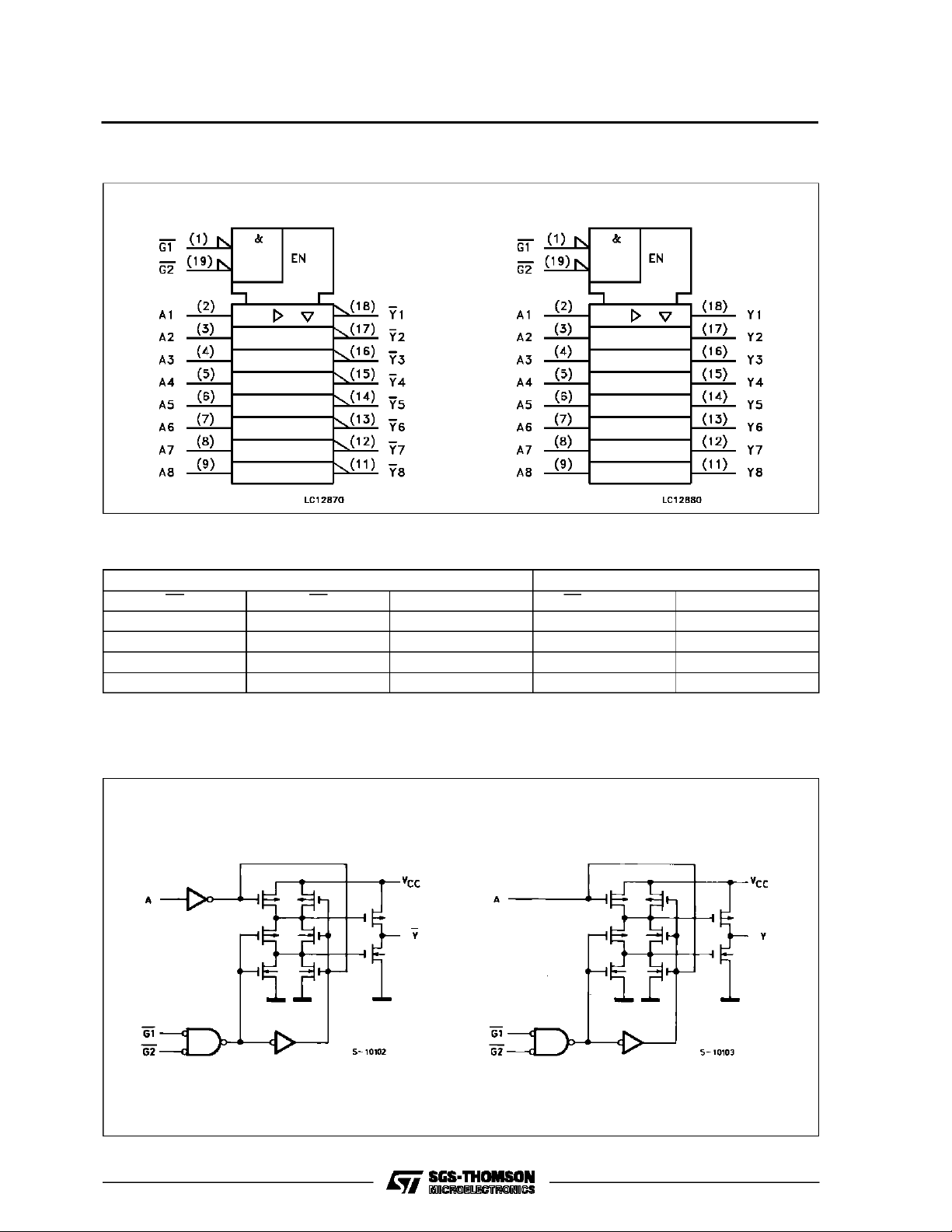
IEC LOGIC SYMBOLS
TRUTH TABLE
M54/M74HCT540/541
HCT541HCT540
INPUT OUTPUT
G1 G2 An Yn (HCT540) Yn (HCT541)
HXXZZ
XHXZZ
LLHLH
X: ”H” or ”L”
Z: Highimpedance
LLLHL
CIRCUIT SCHEMATIC (Per Circuit)
HCT540 HCT541
3/12
Page 4
M54/M74HCT540/541
ABSOLU TE MAXI MUM R AT ING S
Symbol Parameter Value Unit
V
CC
V
V
O
I
IK
I
OK
I
O
I
or I
CC
P
D
T
stg
T
AbsoluteMaximum Ratings arethosevalues beyondwhichdamagetothedevicemayoccur.Functionaloperationundertheseconditionsisnot implied.
(*)500 mW:≅ 65oC derate to300 mW by 10mW/oC: 65oCto85oC
RECO MM ENDED OPERATI N G CONDITIONS
Symbol Parameter Value Unit
V
CC
V
I
V
O
T
op
t
r,tf
Supply Voltage -0.5 to +7 V
DC Input Voltage -0.5 to VCC+ 0.5 V
I
DC Output Voltage -0.5 to VCC+ 0.5 V
DC Input Diode Current ± 20 mA
DC Output Diode Current ± 20 mA
DC Output Source Sink Current Per Output Pin ± 35 mA
DC VCCor Ground Current ± 70 mA
GND
Power Dissipation 500 (*) mW
Storage Temperature -65 to +150
Lead Temperature (10 sec) 300
L
Supply Voltage 4.5 to 5.5 V
Input Voltage 0 to V
Output Voltage 0 to V
Operating Temperature: M54HC Series
M74HC Series
CC
CC
-55 to +125
-40 to +85
Input Rise and Fall Time (VCC= 4.5 to 5.5V) 0 to 500 ns
o
C
o
C
V
V
o
C
o
C
4/12
Page 5

DC SPECIFICATIO NS
Symbol Parameter
V
V
V
V
I
I
∆I
High Level Input
IH
Voltage
Low Level Input
IL
Voltage
High Level
OH
Output Voltage
Low Level Output
OL
Voltage
Input Leakage
I
I
Current
3 State Output
OZ
Off State Current
Quiescent Supply
CC
Current
Additional worst
CC
case supply
current
M54/M74HCT540/541
Test Conditions Value
T
=25oC
V
(V)
4.5
CC
A
54HC and 74HC
Min. Typ. Max. Min. Max. Min. Max.
2.0 2.0 2.0 V
to
5.5
4.5
to
5.5
VI=
IO=-20 µA 4.4 4.5 4.4 4.4
V
IH
4.5
or
I
=-6.0 mA 4.18 4.31 4.13 4.10
O
V
IL
VI=
IO=20µA 0.0 0.1 0.1 0.1
V
IH
4.5
or
I
= 6.0 mA 0.17 0.26 0.33 0.4
O
V
IL
VI=VCCor GND ±0.1 ±1 ±1 µA
5.5
V
5.5
VO=VCCor GND
I=VIH
or V
IL
5.5 VI=VCCor GND 4 40 80 µA
5.5 Per Input pin
VI= 0.5V or
VI= 2.4V
Other Inputs at
V
or GND
CC
-40 to 85oC
74HC
-55 to 125oC
54HC
Unit
0.8 0.8 0.8 V
±0.5 ±5 ±10 µA
2.0 2.9 3.0 mA
V
V
5/12
Page 6

M54/M74HCT540/541
AC ELECTRICAL CHARACTERISTI CS (CL=50pF,Inputtr=tf=6ns)
Test Conditions Value
T
=25oC
Symbol Parameter
t
t
t
t
TLH
THL
PLH
PHL
Output Transition
Time
Propagation
Delay Time
(for HCT540)
t
t
PLH
PHL
Propagation
Delay Time
(for HCT541)
t
PZL
t
PZH
t
PLZ
t
PHZ
C
C
PD
Output Enable
Time
Output Disable
Time
Input Capacitance 5 10 10 10 pF
IN
(*) Power Dissipation
V
C
CC
(V)
L
(pF)
4.5 50 6 12 15 18 ns
4.5 50 12 20 25 30 ns
4.5 150 16 25 31 38 ns
4.5 50 14 23 29 35 ns
4.5 150 18 28 35 42 ns
4.5 50 RL=1KΩ 18 30 38 45 ns
4.5 150 R
=1KΩ 22 34 43 51 ns
L
4.5 50 RL=1KΩ 19 27 34 41 ns
A
54HC and 74HC
Min. Typ. Max. Min. Max. Min. Max.
34
Capacitance
(*) CPDisdefined as the value ofthe IC’s internal equivalent capacitance which is calculated fromthe operating current consumption without load.
(RefertoTest Circuit).Average operting current can be obtained bythefollowingequation. ICC(opr) = CPD•VCC•fIN+ICC/8(per gate)
-40 to 85oC
74HC
-55 to 125oC
54HC
Unit
pF
TEST CIRCUIT ICC(Opr.)
HCT540
6/12
Page 7

SWITCHING CHARACTERISTICS TEST CIRCUIT
HCT540
M54/M74HCT540/541
HCT541
7/12
Page 8

M54/M74HCT540/541
Plastic DIP20 (0.25) MECHANICAL DATA
DIM.
MIN. TYP. MAX. MIN. TYP. MAX.
a1 0.254 0.010
B 1.39 1.65 0.055 0.065
b 0.45 0.018
b1 0.25 0.010
D 25.4 1.000
E 8.5 0.335
e 2.54 0.100
e3 22.86 0.900
F 7.1 0.280
I 3.93 0.155
L 3.3 0.130
Z 1.34 0.053
mm inch
8/12
P001J
Page 9

Ceramic DIP20 MECHANICAL DATA
M54/M74HCT540/541
DIM.
MIN. TYP. MAX. MIN. TYP. MAX.
A 25 0.984
B 7.8 0.307
D 3.3 0.130
E 0.5 1.78 0.020 0.070
e3 22.86 0.900
F 2.29 2.79 0.090 0.110
G 0.4 0.55 0.016 0.022
I 1.27 1.52 0.050 0.060
L 0.22 0.31 0.009 0.012
M 0.51 1.27 0.020 0.050
N1 4° (min.), 15° (max.)
P 7.9 8.13 0.311 0.320
Q 5.71 0.225
mm inch
P057H
9/12
Page 10

M54/M74HCT540/541
SO20 MECHANICAL DATA
DIM.
MIN. TYP. MAX. MIN. TYP. MAX.
A 2.65 0.104
a1 0.10 0.20 0.004 0.007
a2 2.45 0.096
b 0.35 0.49 0.013 0.019
b1 0.23 0.32 0.009 0.012
C 0.50 0.020
c1 45° (typ.)
D 12.60 13.00 0.496 0.512
E 10.00 10.65 0.393 0.419
e 1.27 0.050
e3 11.43 0.450
F 7.40 7.60 0.291 0.299
L 0.50 1.27 0.19 0.050
M 0.75 0.029
S8°(max.)
mm inch
10/12
P013L
Page 11

PLCC20 MECHANICAL DATA
M54/M74HCT540/541
DIM.
MIN. TYP. MAX. MIN. TYP. MAX.
A 9.78 10.03 0.385 0.395
B 8.89 9.04 0.350 0.356
D 4.2 4.57 0.165 0.180
d1 2.54 0.100
d2 0.56 0.022
E 7.37 8.38 0.290 0.330
e 1.27 0.050
e3 5.08 0.200
F 0.38 0.015
G 0.101 0.004
M 1.27 0.050
M1 1.14 0.045
mm inch
P027A
11/12
Page 12

M54/M74HCT540/541
Information furnished is believed to be accurate and reliable.However, SGS-THOMSON Microelectronics assumes no responsability for the
consequences of use of such information nor for any infringement of patents or other rights of third parties which may results from its use. No
license isgranted by implication or otherwise under any patent orpatent rights ofSGS-THOMSON Microelectronics. Specificationsmentioned
in this publication are subject to changewithout notice. This publication supersedes andreplaces all information previously supplied.
SGS-THOMSON Microelectronicsproducts are not authorized foruse ascritical componentsinlife supportdevices orsystemswithout express
written approval of SGS-THOMSON Microelectonics.
1994 SGS-THOMSON Microelectronics - All RightsReserved
Australia - Brazil - France - Germany - Hong Kong - Italy - Japan - Korea - Malaysia - Malta - Morocco - The Netherlands -
Singapore - Spain - Sweden - Switzerland - Taiwan - Thailand - United Kingdom - U.S.A
SGS-THOMSON Microelectronics GROUP OF COMPANIES
12/12
 Loading...