

Page 1
M54/74HCT374
M54/74HCT534
April1993
HCT374 NON INVERTING - HCT534INVERTING
OCTAL D-TYPE FLIP FLOP WITH 3 STATE OUTPUT
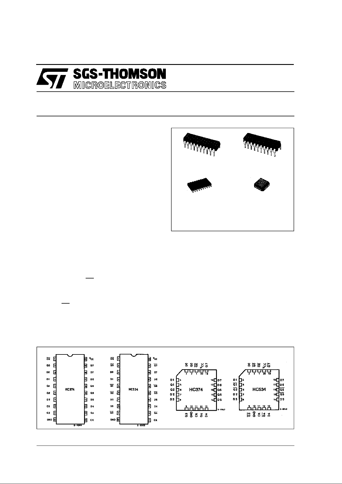
B1R
(PlasticPackage)
ORDER CODES :
M54HC T XXXF1R M74HC T XXXM1R
M74HC T XXXB1R M74HCTXXXC1R
F1R
(CeramicPackage)
M1R
(MicroPackage)
C1R
(Chip Carrier)
PIN CONNECTION (top view)
.HIGH SPEED
f
MAX
= 62 MHz(TYP.) AT VCC=5V
.LOWPOWER DISSIPATION
ICC=4µA(MAX.) AT TA=25°C
.COMPATIBLE WITHTTL OUTPUTS
VIH= 2V (MIN.)VIL= 0.8V (MAX)
.OUTPUT DRIVE CAPABILITY
15 LSTTL LOADS
.SYMMETRICAL OUTPUT IMPEDANCE
IOL=IOH= 6 mA (MIN.)
.BALANCEDPROPAGATION DELAYS
t
PLH=tPHL
.PIN AND FUNCTION COMPATIBLE
WITH 54/74LS374/534
DESCRIPTION
The M54/74HCT374, M54/74HCT534, are high
speed CMOSOCTALD-TYPEFLIPFLOP WITH 3STATE OUTPUTS fabricated with in silicon gate
C2MOS technology. They have the same high
speed performance of LSTTL combined with true
CMOS low power comsuption. These8-bit D-type
flip-flopsarecontrolled by a clockinput (CK)and an
ouput enable input (OE). On the positive transition
of the clock, the Q outputs will be set to the logic
state that were setup at the D inputs (HCT374) or
their complements (HCT534).
While the OEinput is low, the eight outputs will be
in a normal logic state (high or low logic level), and
while high level, the outputs willbe in a high impedancestate.Theoutputcontroldoesnotaffecttheinternaloperationofflip-flops.Thatis,theolddata can
be retained or the new data can be entered even
while the outputs are off. The application engineer
has a choice ofcombinationof inverting andnon-inverting outputs. The 3-state output configuration
and thewide choiceof outline make bus-organized
systemssimple.Allinputs areequipped withprotection circuits against static discharge and transient
excessvoltage. This integrated circuithas inputand
output characteristics that are fully compatible with
54/74 LSTTL logic families. M54/74HCT devices
are designed to directly interface HSC2MOS systems with TTL and NMOS components. They are
also plugin replacements for LSTTL devices giving
a reduction of power consumption.
1/13
Page 2
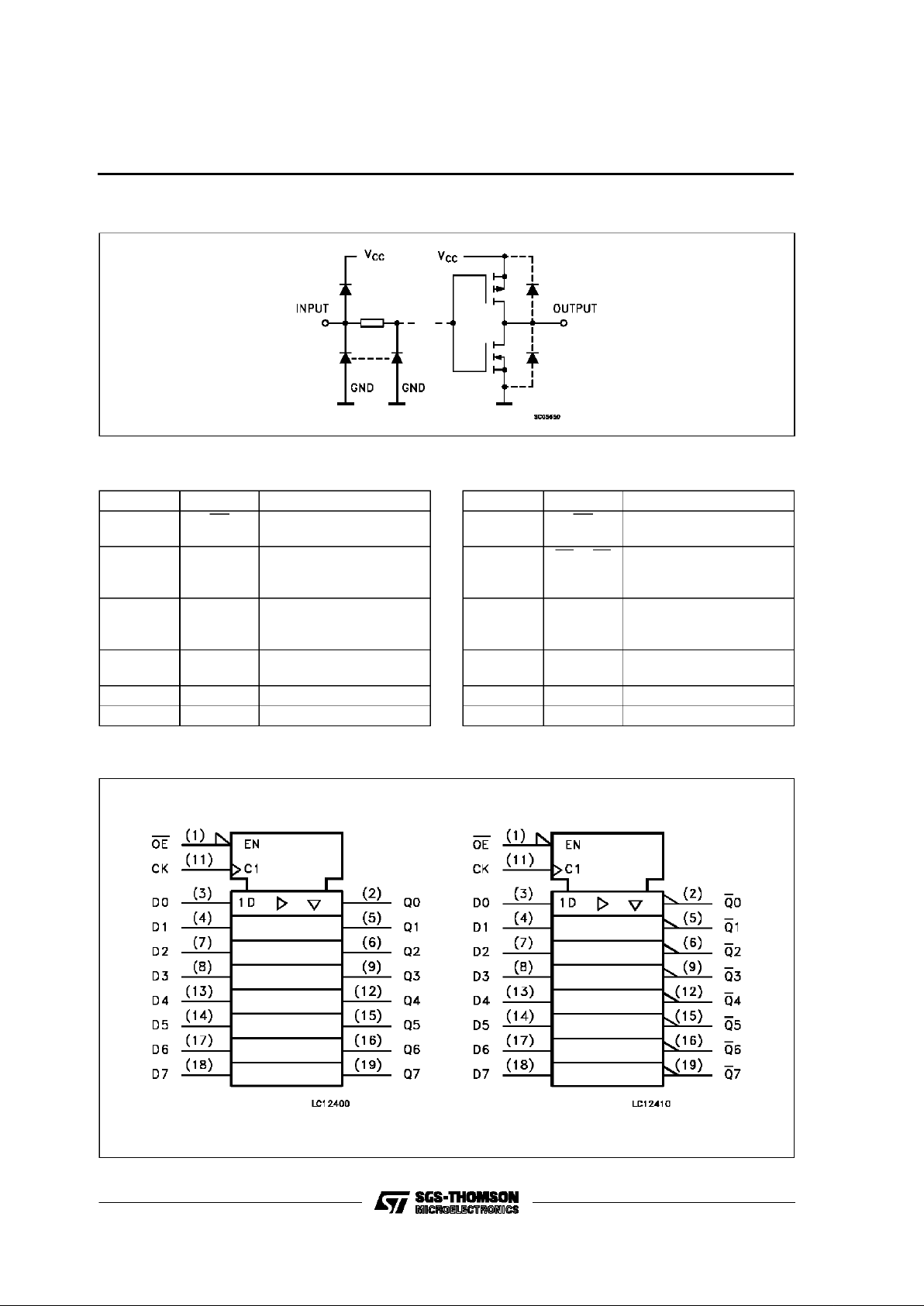
INPUT AND OUTPUT EQUIVALENT CIRCUIT
PIN DESCRIPTION ( HCT374)
PIN No SYMBOL NAME AND FUNCTION
1 OE 3 State output Enable
Input (Active LOW)
2, 5, 6, 9,
12, 15, 16,
19
Q0 to Q7 3 State outputs
3, 4, 7, 8,
13, 14, 17,
18
D0 to D7 Data Inputs
11 CLOCK Clock Input (LOW to
HIGH, edge triggered)
10 GND Ground (0V)
20 V
CC
Positive Supply Voltage
PIN DESCRIPTIO N (HC T534 )
PIN No SYMBOL NAME AND FUNCTION
1 OE 3 State output Enable
Input (Active LOW)
2, 5, 6, 9,
12, 15, 16,
19
Q0 to Q7 3 State outputs
3, 4, 7, 8,
13, 14, 17,
18
D0 to D7 Data Inputs
11 CLOCK Clock Input (LOW to
HIGH, edge triggered)
10 GND Ground (0V)
20 V
CC
Positive Supply Voltage
IEC LOGIC SYMBOLS
HCT374 HCT534
M54/M74HCT374/534
2/13
Page 3
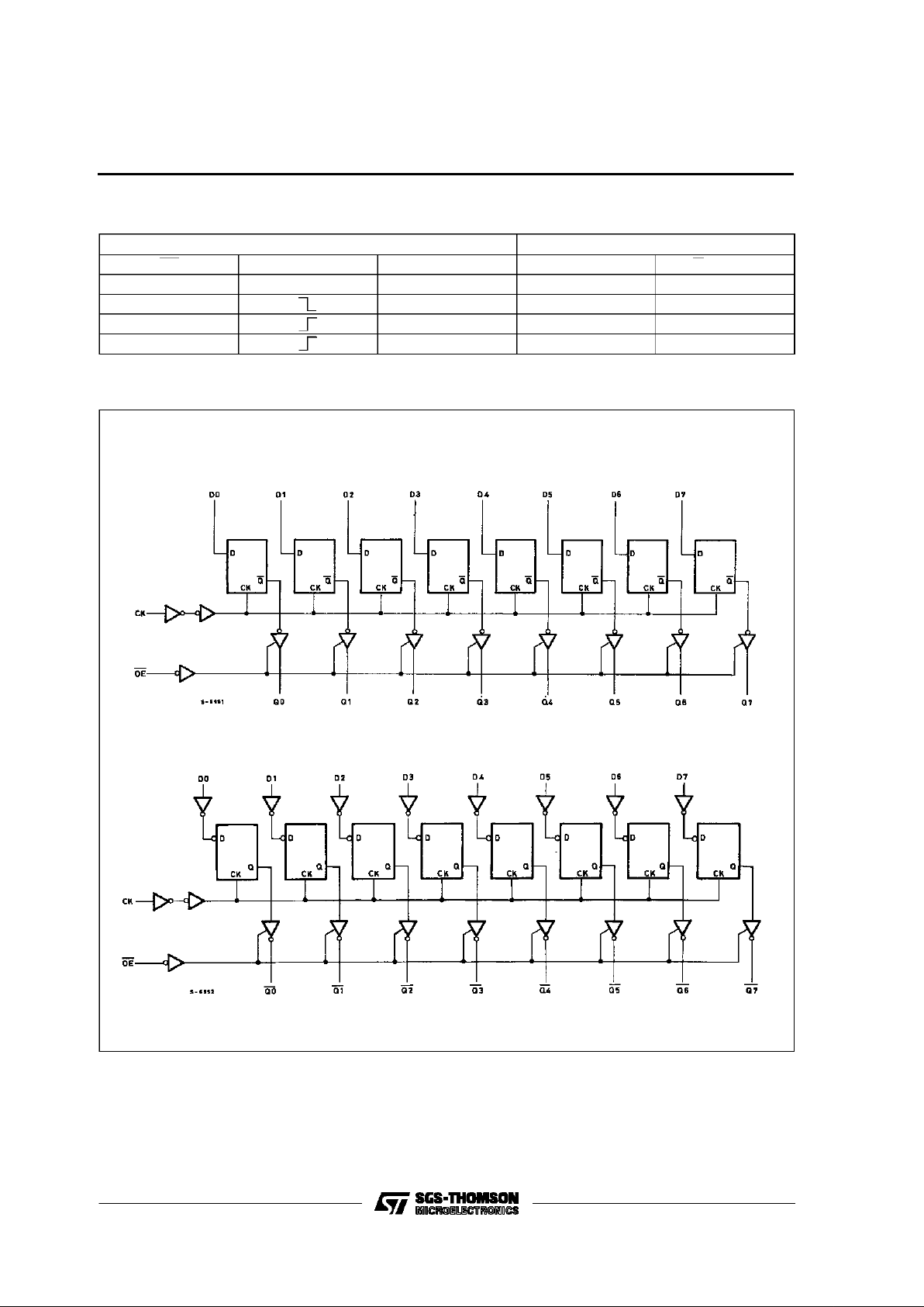
TRUTH TABLE
INPUTS OUTPUTS
OE CK D Q (HC374) Q (HC534)
HXXZZ
L X NO CHANGE NO CHANGE
LLLH
LHHL
LOGIC DIAGRAMS
HCT534
HCT374
M54/M74HCT374/534
3/13
Page 4
ABSOLU TE MAXIMU M R AT I NG S
Symbol Parameter Value Unit
V
CC
Supply Voltage -0.5 to +7 V
V
I
DC Input Voltage -0.5 to VCC+ 0.5 V
V
O
DC Output Voltage -0.5 to VCC+ 0.5 V
I
IK
DC Input Diode Current ± 20 mA
I
OK
DC Output Diode Current ± 20 mA
I
O
DC Output Source Sink Current Per Output Pin ± 35 mA
I
CC
or I
GND
DC VCCor Ground Current ± 70 mA
P
D
Power Dissipation 500 (*) mW
T
stg
Storage Temperature -65 to +150
o
C
T
L
Lead Temperature (10 sec) 300
o
C
AbsoluteMaximumRatingsarethosevalues beyond whichdamage tothedevice mayoccur.Functionaloperationundertheseconditionisnotimplied.
(*)500 mW: ≅ 65oC derate to300mW by 10mW/oC: 65oCto85oC
RECO MM ENDED O PERAT IN G C O NDI TIONS
Symbol Parameter Value Unit
V
CC
Supply Voltage 4.5 to 5.5 V
V
I
Input Voltage 0 to V
CC
V
V
O
Output Voltage 0 to V
CC
V
T
op
Operating Temperature: M54HC Series
M74HC Series
-55 to +125
-40 to +85
o
C
o
C
t
r,tf
Input Rise and Fall Time (VCC= 4.5 to 5.5V) 0 to 500 ns
M54/M74HCT374/534
4/13
Page 5

DC SPECIFICATIO NS
Symbol Parameter
Test Conditions Value
Unit
V
CC
(V)
T
A
=25oC
54HC and 74HC
-40 to 85oC
74HC
-55 to 125oC
54HC
Min. Typ. Max. Min. Max. Min. Max.
V
IH
High Level Input
Voltage
4.5
to
5.5
2.0 2.0 2.0 V
V
IL
Low Level Input
Voltage
4.5
to
5.5
0.8 0.8 0.8 V
V
OH
High Level
Output Voltage
4.5
VI=
V
IH
or
V
IL
IO=-20 µA 4.4 4.5 4.4 4.4
V
I
O
=-6.0 mA 4.18 4.31 4.13 4.10
V
OL
Low Level Output
Voltage
4.5
VI=
V
IH
or
V
IL
IO=20µA 0.0 0.1 0.1 0.1
V
I
O
= 6.0 mA 0.17 0.26 0.33 0.4
I
I
Input Leakage
Current
5.5
VI=VCCor GND ±0.1 ±1 ±1 µA
I
CC
Quiescent Supply
Current
5.5 VI=VCCor GND 4 40 80 µA
∆I
CC
Additional worst
case supply
current
5.5 Per Input pin
VI= 0.5V or
V
I
= 2.4V
Other Inputs at
VCCor GND
IO=0
2.0 2.9 3.0 mA
M54/M74HCT374/534
5/13
Page 6

AC ELECTRICAL CHARACTERISTICS (CL=50pF,Inputtr=tf=6ns)
Symbol Parameter
Test Conditions Value
Unit
V
CC
(V)
C
L
(pF)
T
A
=25oC
54HC and 74HC
-40 to 85oC
74HC
-55 to 125oC
54HC
Min. Typ. Max. Min. Max. Min. Max.
t
TLH
t
THL
Output Transition
Time
4.5 50 7 12 15 18
ns
t
PLH
t
PHL
Propagation
Delay Time
(CLOCK - Q, Q)
4.5 50 20 30 38 45 ns
4.5 150 25 38 48 57
ns
t
PZL
t
PZH
Output Enable
Time
4.5 50 RL=1KΩ 17 30 38 45 ns
4.5 150 R
L
=1KΩ 25 38 48 57 ns
t
PZL
t
PZH
Output Disable
Time
4.5 50 RL=1KΩ 16 28 35 42
ns
f
MAX
Maximum CLock
Frequency
4.5 50 31 50 25 21
ns
t
W(L)
t
W(H)
Minimum Pulse
Width (CLOCK)
4.5 50 15 19 23
ns
t
s
Minimum Set-up
Time
4.5 50 15 19 23
ns
t
h
Minimum Hold
Time
4.5 50 0 0 0
ns
C
IN
Input Capacitance 5 10 10 10 pF
C
OUT
Out put
Capacitance
10
pF
C
PD
(*) Power Dissipation
Capacitance
48
pF
(*) CPDisdefined as the valueof the IC’s internal equivalent capacitance which is calculatedfromthe operatingcurrent consumption withoutload.
(Refer toTest Circuit).Averageoperting current can be obtainedby the followingequation.ICC(opr) = CPD•VCC•fIN+ICC/8 (per FLIP-FLOP)andC
PD
when N pcs ofFLIP-FLOPoperate, can begainedbyfollowing equation:CPD(TOTAL)=38 + 18 x N (pF)
M54/M74HCT374/534
6/13
Page 7

SWITCHING CHARACTERISTICS TEST WAVEFORM
t
PLZ,tPZL
The 1KΩ load resistors should be connected between
outputs and VCCline and the 50pF load capacitors
should be connected between outputsand GND line.
All inputs except OE input should be connected to V
CC
line or GND line such that outputs will be in low logic
level while OE input is held low.
t
PHZ,tPZH
The 1KΩ load resistors and the 50pF load capacitors
should be connected between each output and GND
line.
All inputs except OE input should be connected to V
CC
or GND line such that output will be in high logic level
while OE input is held low.
t
PLH,tPHL,ts,th,tw
f
MAX
M54/M74HCT374/534
7/13
Page 8

TEST CIRCUIT ICC(Opr.)
INPUTWAVEFORM IS THE SAMEAS THATIN CASEOFSWITCHING CHARACTERISTICSTEST.
M54/M74HCT374/534
8/13
Page 9

Plastic DIP20 (0.25) MECHANICAL DATA
DIM.
mm inch
MIN. TYP. MAX. MIN. TYP. MAX.
a1 0.254 0.010
B 1.39 1.65 0.055 0.065
b 0.45 0.018
b1 0.25 0.010
D 25.4 1.000
E 8.5 0.335
e 2.54 0.100
e3 22.86 0.900
F 7.1 0.280
I 3.93 0.155
L 3.3 0.130
Z 1.34 0.053
P001J
M54/M74HCT374/534
9/13
Page 10

Ceramic DIP20 MECHANICAL DATA
DIM.
mm inch
MIN. TYP. MAX. MIN. TYP. MAX.
A 25 0.984
B 7.8 0.307
D 3.3 0.130
E 0.5 1.78 0.020 0.070
e3 22.86 0.900
F 2.29 2.79 0.090 0.110
G 0.4 0.55 0.016 0.022
I 1.27 1.52 0.050 0.060
L 0.22 0.31 0.009 0.012
M 0.51 1.27 0.020 0.050
N1 4° (min.), 15° (max.)
P 7.9 8.13 0.311 0.320
Q 5.71 0.225
P057H
M54/M74HCT374/534
10/13
Page 11

SO20 MECHANICAL DATA
DIM.
mm inch
MIN. TYP. MAX. MIN. TYP. MAX.
A 2.65 0.104
a1 0.10 0.20 0.004 0.007
a2 2.45 0.096
b 0.35 0.49 0.013 0.019
b1 0.23 0.32 0.009 0.012
C 0.50 0.020
c1 45° (typ.)
D 12.60 13.00 0.496 0.512
E 10.00 10.65 0.393 0.419
e 1.27 0.050
e3 11.43 0.450
F 7.40 7.60 0.291 0.299
L 0.50 1.27 0.19 0.050
M 0.75 0.029
S8°(max.)
P013L
M54/M74HCT374/534
11/13
Page 12

PLCC20 MECHANICAL DATA
DIM.
mm inch
MIN. TYP. MAX. MIN. TYP. MAX.
A 9.78 10.03 0.385 0.395
B 8.89 9.04 0.350 0.356
D 4.2 4.57 0.165 0.180
d1 2.54 0.100
d2 0.56 0.022
E 7.37 8.38 0.290 0.330
e 1.27 0.050
e3 5.08 0.200
F 0.38 0.015
G 0.101 0.004
M 1.27 0.050
M1 1.14 0.045
P027A
M54/M74HCT374/534
12/13
Page 13

Information furnished is believed to be accurate and reliable.However, SGS-THOMSON Microelectronics assumes no responsability for the
consequences of use of such information nor for any infringement of patents or other rights of third parties which may results from its use. No
license is grantedbyimplication or otherwise underany patentorpatentrights ofSGS-THOMSON Microelectronics. Specificationsmentioned
in this publicationaresubject to change without notice.Thispublication supersedes and replaces all information previously supplied.
SGS-THOMSON Microelectronicsproductsare notauthorizedforuse ascritical componentsinlife support devicesorsystems withoutexpress
written approval of SGS-THOMSON Microelectonics.
1994 SGS-THOMSON Microelectronics- All RightsReserved
SGS-THOMSON Microelectronics GROUPOF COMPANIES
Australia - Brazil - France - Germany - Hong Kong - Italy - Japan - Korea - Malaysia - Malta - Morocco - The Netherlands -
Singapore - Spain - Sweden - Switzerland - Taiwan - Thailand - UnitedKingdom - U.S.A
M54/M74HCT374/534
13/13
 Loading...