

Datasheet M74HCT4053TTR, M74HCT4053RM13TR, M74HCT4053M1R, M74HCT4053B1R Datasheet (SGS Thomson Microelectronics)
Page 1

M74HCT4053
TRIPLE 2-CHANNEL
ANALOG MULTIPLEXER/DEMULTIPLEXER
■ LOW POWER DISSIPATION:
I
= 4µA (MAX.) at TA=25°C
CC
■ LOGIC LEVEL TRANSLATION TO ENABLE
TTL LOGIC SIGNAL TO COMMUNICATE
WITH ±5V ANALOG SIGNAL
■ LOW "ON" RESISTANCE:
70Ω TY P. (V
50Ω TY P. (V
■ WIDE ANALOG INPUT VOLTAGE RANGE:
- VEE = 4.5V)
CC
- VEE = 9V)
CC
±6V
■ FAST SWITCHING :
t
= 13ns (TYP.) at TA = 25 °C
pd
■ LOW CROSSTALK BETWEEN SWITCHES
■ HIGH ON/OFF OUTPUT VOL TAGE RATIO
■ WIDE OPERATING SUPPLY VOLTAGE
RANG E (V
■ LOW SINE WAVE DISTORTION:
0.02% at V
■ COMPATIBLE WI TH TTL OUTPUTS:
V
= 2V(MIN.) VIL = 0.8V (MAX.)
IH
■ PIN AND FUNCTION COMPATIBLE WITH
- VEE) = 2V TO 12V
CC
- VEE = 9V
CC
74 SERIES 4053
DESCRIPTION
The M74HCT4053 is a triple two-channel anal og
MULTIPLEXER/DEMULTIPLEXER fabricated
with silicon gate C
2
MOS technology and it is pin
to pin compatible with the equ ivalent metal gate
CMOS4000B series.
It contains 6 bidirectional and digitally controlled
analog switches.
PIN CONNECTION AND IEC LOGIC SYMBOLS
TSSOPDIP SOP
ORDER CODES
P ACKAGE TUBE T & R
DIP
SOP
TSSOP
M74HCT4053B1R
M74HCT4053M1R M74HCT4053RM13TR
M74HCT4053TTR
A built-in level shifting is included to allow an input
range up to ±6V (peak) for an analog signal with
digital control signal of 0 to 6V.
V
supply pin is provided for analog input
EE
signals. It has an inhibit (INH) input terminal to
disable all the switches when high, compatible
with TTL output level. For operation as a digital
multiplexer/demultiplexer, VEE is connected to
GND. A, B and C control inputs select one of a pair
of channels, they are compatibl e with TTL output
level.
All inputs are equipped with protection circuits
against static discharge and transient excess
voltage.
1/12September 2001
Page 2
M74HCT4053
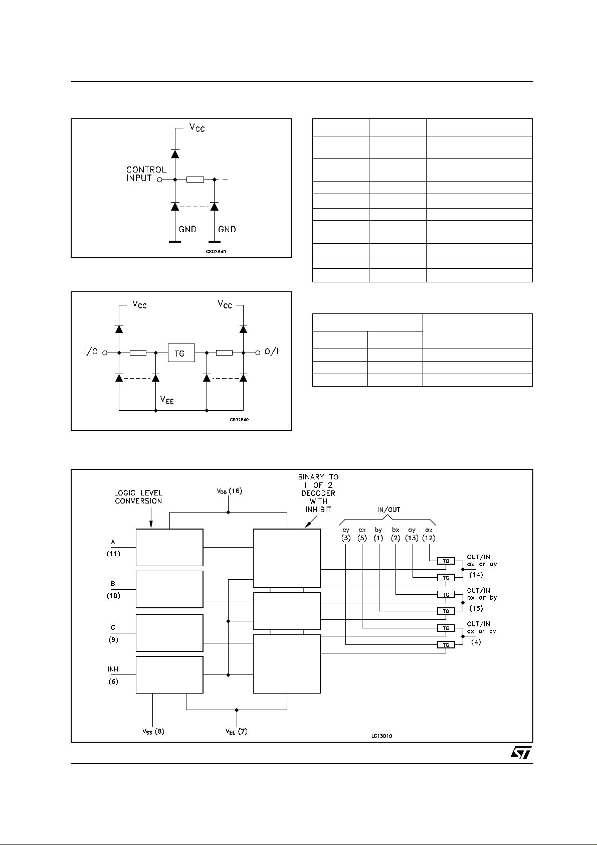
CONTROL INPUT EQUIVALENT CIRCUIT
I/O EQUIVALENT CIRCUIT
PIN DESCRIPTION
PIN No SYMBOL NAME AND FUNCTION
2, 1 bx, by Independent Input Out-
5, 3 cx, cy Independent Input Out-
6 INH INHIBIT Input
7V
11, 10, 9 A, B, C Select Inputs
12, 13 ax, ay Independent Input Out-
14, 15, 4 ax to cy Common Output/Input
8 GND Ground (0V)
16 V
EE
CC
puts
puts
Negative Supply Voltage
puts
Positive Supply Voltage
TRUTH TABLE
INPUT STATE
INH A or B or C
L L ax or bx or cx
L H ay or by or cy
H X NONE
ON CHANNEL
FUNCTIONAL DIAGRAM
2/12
Page 3
M74HCT4053
ABSOLUTE MAXIMUM RATINGS
Symbol Parameter Value Unit
V
V
CC - VEE
V
V
I
CK
I
IOK
I
I
or I
CC
P
T
T
Absolute Maximum Ratings are those values beyond which damage to the device may occur. Functional operation under these conditions is
not implied
(*) 500mW at 65
RECOMMENDED OPERATING CONDITIONS
Symbol Parameter Value Unit
V
V
V
CC - VEE
V
V
T
t
r
Supply Voltage
CC
Supply Voltage
Control Input Voltage -0.5 to VCC + 0.5
I
Switch I/O Voltage V
I/O
EE
Control Input Diode Current
I/O Diode Current
Switch Through Current
T
DC VCC or Ground Current
GND
Power Dissipation
D
Storage Temperature
stg
Lead Temperature (10 sec)
L
°C; derate to 300mW by 10mW/°C from 65°C to 85°C
Supply Voltage
CC
Supply Voltage
EE
Supply Voltage
Input Voltage 0 to V
I
I/O Voltage VEE to V
I/O
Operating Temperature
op
, t
Input Rise and Fall Time VCC = 4.5 to 5.5V
f
-0.5 to +7 V
-0.5 to +13 V
-0.5 to VCC + 0.5
± 20 mA
± 20 mA
± 25 mA
± 50 mA
500(*) mW
-65 to +150 °C
300 °C
4.5 to 5.5 V
-6 to 0 V
2 to 12 V
CC
CC
-55 to 125 °C
0 to 500 ns
V
V
V
V
3/12
Page 4
M74HCT4053
DC SPECIFICATIONS
Test Condition Value
Symbol Parameter
V
V
R
∆R
High Level Input
IHC
Voltage
Low Level Input
ILC
Voltage
ON Resistance 4.5 GND VI = V
ON
Difference of ON
ON
Resistance
between switches
I
Input/Output
OFF
Leakage Current
(SWITCH OFF)
Switch Input
I
IZ
Leakage Current
(SWITCH ON,
OUTPUT OPEN)
I
Input Leakage
I
Current
I
Quiescent Supply
CC
Current
∆I
Additional
CC
Quiescent Supply
Current per input
pin
V
(V)
CC
V
(V)
EE
T
= 25°C
A
-40 to 85°C
Min. Typ. Max. Min. Max. Min. Max.
-55 to
125°C
4.5
to
2.0 2.0 2.0 V
5.5
4.5
to
0.8 0.8 0.8 V
5.5
or V
IHC
V
= VCC to V
4.5 -4.5 55 120 150 180
4.5 G ND V
4.5 -4.5 50 100 125 150
4.5 GND VI = V
4.5 -4.5 5 12 15 18
I/O
I
I/O
= V
I
V
= VCC or V
I/O
I
I/O
V
= VCC or V
I/O
I
I/O
≤ 2mA
IHC
≤ 2mA
IHC
≤ 2mA
or V
or V
ILC
EE
ILC
EE
ILC
EE
5.5 GND VOS = VCC or GND
5.5 -6.0
IS
VI = V
ILC
or V
CC
IHC
V
= GND or V
5.5 GND VOS = VCC or GND
V
= V
or V
I
5.5 -6.0
IHC
ILC
85 180 225 270
70 150 190 230
10 30 35 45
±
0.06
± 0.6 ± 1.0
± 0.1 ± 1 ± 1
±
0.06
± 0.6 ± 1.0
± 0.1 ± 1 ± 1
5.5 GND VI = VCC or GND ± 0.1 ± 0.1 ± 1
5.5 GND
5.5 -6.0 8 80 160
4.5
to
5.5
GND
V
= VCC or GND
I
= VCC - 2.1V
V
I
other input at V
or GND
CC
100 360 450 490 µA
44080
Unit
Ω
Ω
µA
µA
µA
µA
4/12
Page 5

AC ELECTRICAL CHARACTERISTICS (CL = 50 pF, Input tr = tf = 6ns)
Test Condition Value
M74HCT4053
Symbol Parame ter
Φ
Phase Difference
I/O
Between Input and
Output
t
Output Enable
PZL
PZH
t
PLZ
PHZ
Time
Output Disable
Time
t
t
T
= 25°C
V
V
CC
EE
(V)
(V)
4.5 GND
= 50pF
C
4.5 -4.5 4 8 10 12
L
4.5 GND RL = 1KΩ
C
4.5 -4.5 11 34 43 51
= 50pF
L
4.5 GND RL = 1KΩ
C
4.5 -4.5 19 31 39 47
= 50pF
L
A
Min. Typ. Max. Min. Max. Min. Max.
512 15 18
13 45 56 68
25 38 48 58
-40 to 85°C
-55 to
125°C
Unit
ns
ns
ns
CAPACITANCE CHARACTERISTICS
Test Condition Value
Symbol Parameter
C
Input Capacitance 5.0 5 10 10 10 pF
IN
C
C
C
C
Common Terminal
I/O
Capacitance
Switch Terminal
I/O
Capacitance
Feed Through
IOS
Capacitance
Power Dissipation
PD
Capacitance
= 25°C
V
(V)
CC
V
(V)
EE
A
Min. Typ. Max. Min. Max. Min. Max.
5.0 -5.0 11 20 20 20 pF
5.0 -5.0 7 15 15 15 pF
5.0 -5.0 0.75 2 2 2 pF
5.0 GND 67 pF
-40 to 85°C
T
(note 1)
1) CPD is defined as the value of the IC’s internal equivalent capacitance which is calculated from the operating current consumption without
load. (R ef er to Test Circ ui t ). Average operating cu rrent can be ob ta i ned by the following equat ion. I
= CPD x VCC x fIN + ICC
CC(opr)
-55 to
125°C
Unit
5/12
Page 6

M74HCT4053
ANALOG SWITCH CHARACTERISTICS (GND = 0V;TA = 25°C)
Symbol Parameter Test Condition Value Unit
V
V
CC
(V)
V
(V)
EE
(V
IN
p-p
)
Typ.
Sine Wave
Distortion
Sine Wave
Distortion
f
MAX
Frequency
Response
(Switch ON) (*)
f
MAX
Frequency
Response
(Switch ON) (**)
Feed through
Attenuation
(Switch OFF)
Crosstalk (Control
Input to Signal
Output)
Crosstalk
(between any two
switches)
(*) Inpu t COMMON Term i nal, and me asured at SWITCH Terminal
(**) In put SWIT CH T ermin al , and measured at common Term i na l
NOTE: T hese characte ri stics are determined by the design of the device.
2.25 -2.25 4
4.5 -4.5 8 0.020
2.25 -2.25 4
4.5 -4.5 8 0.06
f
2.25 -2.25 Adjust fIN voltage to obtain 0 dBm at VOS.
Increase f
IN
R
= 50Ω, CL = 10 pF, fIN = 1KHz sine wave
L
2.25 -2.25 Adjust fIN voltage to obtain 0 dBm at VOS.
Increase f
6.0 -6.0
IN
R
= 50Ω, CL = 10 pF, fIN = 1KHz sine wave
L
2.25 -2.25 V
4.5 -4.5 -50
R
= 600Ω, CL = 50 pF, fIN = 1MHz sine wave
L
4.5 0 Adjust R
R
4.5 -4.5 140
= 600Ω, CL = 50 pF, fIN = 1MHz square wave between
L
2.25 -2.25 Adjust V
R
4.5 -4.5 -50
= 600Ω, CL = 50 pF, fIN = 1MHz sine wave
L
f
= 1 KHz RL = 10 KΩ, CL = 50 pF
IN
= 10 KHz RL = 10 KΩ, CL = 50 pF
IN
Frequency until dB meter reads -3dB
Frequency until dB meter reads -3dB
is centered at (VCC - VEE)/2
IN
Adjust input for 0 dBm
at set up so that IS = 0A.
L
Vcc and GND tr=tf= 6 ns
to obtain 0dBm at input
IN
0.025
0.12
120
95
-50
60
-50
%
%
MHz4.5 -4.5 190
MHz4.5 -4.5 150
dB
mV
dB
6/12
Page 7

M74HCT4053
SWITCHING CARACTERISTICS TEST CIRCUIT
CROSSTALK (control to output)
BANDWIDTH AND FEEDTHROUGH ATTENUATION CROSSTALK BETWEEN ANY TWO SWITCHES
7/12
Page 8

M74HCT4053
SWITCHING CHARACTERISTICS WAVEFORM
CHANNEL RESISTANCE (R
8/12
ICC (Opr.)
ON)
Page 9

M74HCT4053
Plastic DIP-16 (0.25) MECHANICAL DATA
mm. inch
DIM.
MIN. TYP MAX. MIN. TYP. MAX.
a1 0.51 0.020
B 0.77 1.65 0.030 0.065
b 0.5 0.020
b1 0.25 0.010
D 20 0.787
E 8.5 0.335
e 2.54 0.100
e3 17.78 0.700
F 7.1 0.280
I 5.1 0.201
L 3.3 0.130
Z 1.27 0.050
P001C
9/12
Page 10

M74HCT4053
SO-16 MECHANICAL DATA
DIM.
A 1.75 0.068
a1 0.1 0.2 0.003 0.007
a2 1.65 0.064
b 0.35 0.46 0.013 0.018
b1 0.19 0.25 0.007 0.010
C 0.5 0.019
c1 45° (typ.)
D 9.8 10 0.385 0.393
E 5.8 6.2 0.228 0.244
e 1.27 0.050
e3 8.89 0.350
F 3.8 4.0 0.149 0.157
G 4.6 5.3 0.181 0.208
L 0.5 1.27 0.019 0.050
M 0.62 0.024
S8° (max.)
MIN. TYP MAX. MIN. TYP. MAX.
mm. inch
10/12
PO13H
Page 11

M74HCT4053
TSSOP16 MECHANICAL DATA
mm. inch
DIM.
MIN. TYP MAX. MIN. TYP. MAX.
A 1.2 0.047
A1 0.05 0.15 0.002 0.004 0.006
A2 0.8 1 1.05 0.031 0.039 0.041
b 0.19 0.30 0.007 0.012
c 0.09 0.20 0.004 0.0089
D 4.9 5 5.1 0.193 0.197 0.201
E 6.2 6.4 6.6 0.244 0.252 0.260
E1 4.3 4.4 4.48 0.169 0.173 0.176
e 0.65 BSC 0.0256 BSC
K0° 8°0° 8°
L 0.45 0.60 0.75 0.018 0.024 0.030
A2
A
A1
b
e
c
K
L
E
D
E1
PIN 1 IDENTIFICATION
1
0080338D
11/12
Page 12

M74HCT4053
Information furnished is bel ieved to be accurate and reliable. However, STMicroe lectronics assumes no responsibility for the
consequences of use of such information nor for any infringement of patents or other rights of third parties which may result from
its use. No li cense is granted by imp lica tion or otherwise under any patent or patent rig hts of STMicroelectronics. Specificat ions
mentioned in this publication ar e subject to change without notice. This publication supersedes and replaces all information
previously supplied. S TMicroelectronics products are not authorized for use as critica l components in life suppo rt devices or
systems without express written approval of STMicroelectronics.
Australi a - Brazil - Chi na - Finland - F rance - Germany - Hong Kon g - India - Italy - Japan - Malay si a - Malta - Morocco
© The ST logo is a registered trademark of STMicroelectronics
© 2001 STM icroelectronics - Printed in Ital y - All Rights Reserved
STMicr o el ectronics GROUP OF COMPA NI E S
Singapo re - Spain - Sweden - Switzerland - Un i ted Kingdom
© http://www.st.com
12/12
 Loading...