

Page 1
.HIGH SPEED
f
= 80 MHz(TYP.) ATVCC=5V
MAX
.LOWPOWER DISSIPATION
ICC=4µA(MAX.) AT TA=25°C
.COMPATIBLE WITHTTL OUTPUTS
VIH= 2V (MIN.) VIL= 0.8V (MAX)
.OUTPUT DRIVE CAPABILITY
10 LSTTL LOADS
.SYMMETRICALOUTPUT IMPEDANCE
|IOH|=IOL=4 mA (MIN.)
.BALANCEDPROPAGATION DELAYS
t
PLH=tPHL
.PIN AND FUNCTION COMPATIBLE
WITH 54/74LS393
M54HCT393
M74HCT393
DUAL BINARY COUNTER
B1R
(PlasticPackage)
M1R
(MicroPackage)
ORDER CODES :
M54HC T393F1R M74H CT393M1R
M74HC T393B1R M74HCT393C1R
F1R
(CeramicPackage)
C1R
(Chip Carrier)
DESCRIPTION
The M54/74HCT393is a high speed CMOSDUAL
BINARY COUNTER fabricated in silicon gate
C2MOS technology. It has the same high speed
performance of LSTTL combined with true COMS
low power consumption.
This counter circuit contains independent ripple
carry counters and two 4-bit ripple carry binary
counters, which can be cascated to create a single
divideby 256 counter.
Each4-bit counter isincremented on the hightolow
transition (negative edge) of the clock input,and
eachhas an independent clear input. When clearis
set to high all four bits of each counter are setto a
low level. This enables counttruncation and allows
the implementation of divide by N counter
configurations.
This integrated circuit has input and output
characteristics that are fully compatible with 54/74
LSTTL logic families. M54/74HCT devices are
designed to directly interface HSC2MOS systems
with TTL and NMOS components. They are also
plug in replacements for LSTTL devices giving a
reduction of power consumption.
All inputs are equipped with protection circuits
against static discharge and transient excess
voltage.
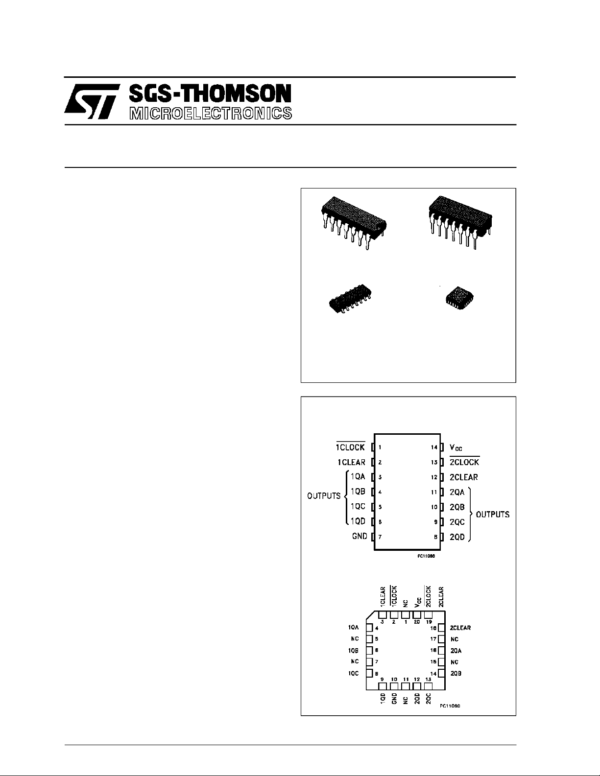
PIN CONNECTIONS(top view)
NC =
No Internal
Connection
October 1993
1/12
Page 2
M54/M74HCT393
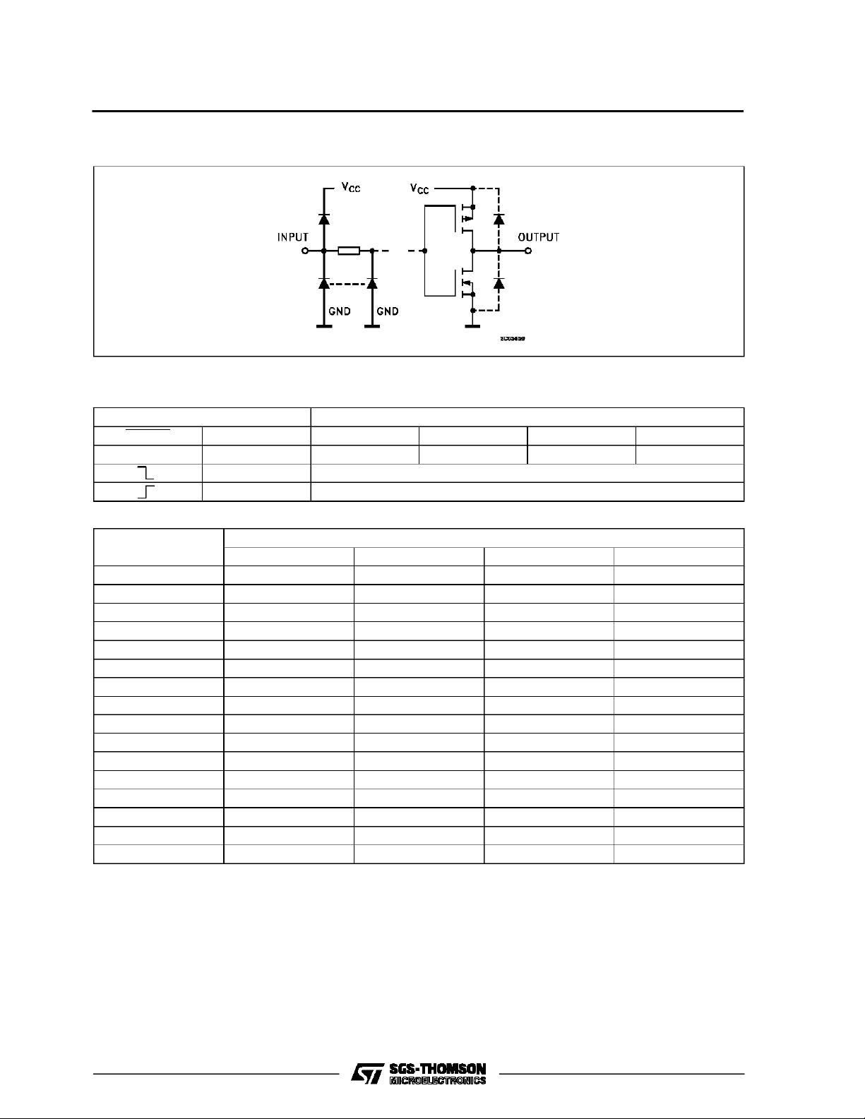
INPUT AND OUTPUT EQUIVALENT CIRCUIT
TRUTH TABLE
INPUTS OUTPUS
CLOCK CLEAR QD QC QB QA
XHLLLL
L COUNT UP
L NO CHANGE
X:Don’t Care
COUNT
0LLLL
1LLLH
2LLHL
3LLHH
4LHLL
5LHLH
6LHHL
7LHHH
8HLLL
9HLLH
10HLHL
11 H L H H
12 H H L L
13HHLH
14 H H H L
15HHHH
QD QC QB QA
OUTPUT
2/12
Page 3
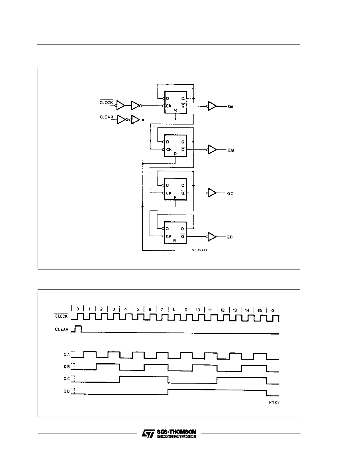
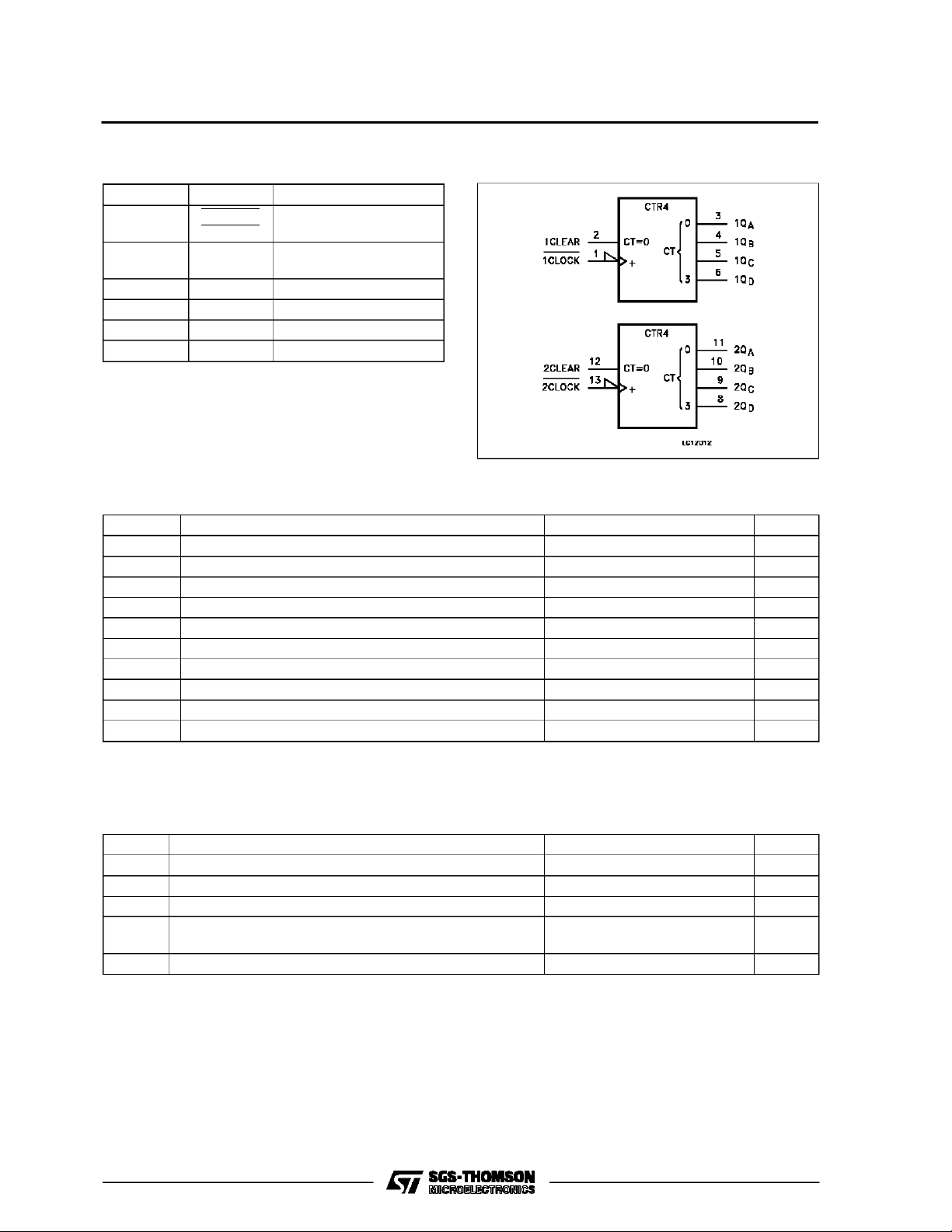
LOGI C DI AGRAM
M54/M74HCT393
TIM ING C HAR T
3/12
Page 4
M54/M74HCT393
PIN DESCRIPTION
IEC LOGIC SYMBOL
PIN No SYMBOL NAME AND FUNCTION
1, 13 1 CLOCK
2 CLOCK
2, 12 1 CLEAR
2 CLEAR
Clock Input (HIGH to
LOW Edge triggered)
Asynchronouns Master
Reset Inputs
3, 4, 5, 6 1QA to 1QD Flip Flop Outputs
11, 10, 9, 8 2QA to 2QD Flip Flop Outputs
7 GND Ground (0V)
14 V
CC
Positive Supply Voltage
ABSOLU TE M AXIMU M R AT INGS
Symbol Parameter Value Unit
V
CC
V
V
O
I
IK
I
OK
I
O
or I
I
CC
P
D
T
stg
T
L
AbsoluteMaximumRatingsarethose values beyond whichdamagetothedevicemayoccur.Functional operation under theseconditionisnotimplied.
(*)500 mW: ≅ 65oC derate to300mW by 10mW/oC: 65oCto85oC
Supply Voltage -0.5 to +7 V
DC Input Voltage -0.5 to VCC+ 0.5 V
I
DC Output Voltage -0.5 to VCC+ 0.5 V
DC Input Diode Current ± 20 mA
DC Output Diode Current ± 20 mA
DC Output Source Sink Current Per Output Pin ± 25 mA
DC VCCor Ground Current ± 50 mA
GND
Power Dissipation 500 (*) mW
Storage Temperature -65 to +150
Lead Temperature (10 sec) 300
o
C
o
C
RECO MM ENDED OPERATI N G CO NDI TIONS
Symbol Parameter Value Unit
Supply Voltage 4.5 to 5.5 V
CC
Input Voltage 0 to V
I
Output Voltage 0 to V
O
Operating Temperature: M54HC Series
op
M74HC Series
CC
CC
-55 to +125
-40 to +85
Input Rise and Fall Time (VCC= 4.5 to 5.5V) 0 to 500 ns
4/12
V
T
t
V
V
r,tf
V
V
o
C
o
C
Page 5

DC SPECIFICATIONS
Symbol Parameter
V
V
V
V
I
∆I
High Level Input
IH
Voltage
Low Level Input
IL
Voltage
High Level
OH
Output Voltage
Low Level Output
OL
Voltage
Input Leakage
I
I
Current
Quiescent Supply
CC
Current
Additional worst
CC
case supply
current
M54/M74HCT393
Test Conditions Value
T
=25oC
V
(V)
4.5
CC
A
54HC and 74HC
Min. Typ. Max. Min. Max. Min. Max.
2.0 2.0 2.0 V
to
5.5
4.5
to
5.5
VI=
IO=-20 µA 4.4 4.5 4.4 4.4
V
IH
4.5
or
I
=-4.0 mA 4.18 4.31 4.13 4.10
O
V
IL
VI=
IO=20µA 0.0 0.1 0.1 0.1
V
IH
4.5
or
I
= 4.0 mA 0.17 0.26 0.33 0.4
O
V
IL
VI=VCCor GND ±0.1 ±1 ±1 µA
5.5
5.5 VI=VCCor GND 4 40 80 µA
5.5 Per Input pin
VI= 0.5V or
V
= 2.4V
I
Other Inputs at
VCCor GND
-40 to 85oC
74HC
-55 to 125oC
54HC
Unit
0.8 0.8 0.8 V
2.0 2.9 3.0 mA
V
V
5/12
Page 6

M54/M74HCT393
AC ELECTRICAL CHARACTERISTICS (CL=50pF,Inputtr=tf=6ns)
Test Conditions Value
T
=25oC
Symbol Parameter
t
TLH
t
THL
t
PLH
t
PHL
Output Transition
Time
Propagation
Delay Time
V
CC
(V)
4.5 8151922ns
4.5 19 30 38 45 ns
A
54HC and 74HC
Min. Typ. Max. Min. Max. Min. Max.
(CLOCK - QA)
t
t
PLH
PHL
Propagation
Delay Time
4.5 24 37 46 56 ns
(CLOCK - QB)
t
t
PLH
PHL
Propagation
Delay Time
4.5 28 43 54 65 ns
(CLOCK - QC)
t
t
PLH
PHL
Propagation
Delay Time
4.5 33 51 64 77 ns
(CLOCK - QD)
t
t
PLH
PHL
Propagation
Delay Time
4.5 20 31 39 47 ns
(CLEAR - Qn)
f
MAX
Maximum Clock
4.5 4.2 80 34 MHz
Frequency
t
W(H)
t
W(L)
Minimum Pulse
Width
4.5 8151922ns
(CLOCK)
t
W(H)
Minimum Pulse
4.5 8151922ns
Width
(CLEAR)
t
REM
Minimum
4.5 5 6 8 ns
Removal Time
C
C
PD
Input Capacitance 5 10 10 10 pF
IN
(*) Power Dissipation
66
Capacitance
(*) CPDisdefined as the valueof the IC’s internal equivalent capacitance whichis calculated from the operatingcurrent consumption without load.
(Referto Test Circuit).Average opertingcurrentcan be obtained bythe followingequation. ICC(opr) = CPD•VCC•fIN+ICC/4(per Flip Flop)
-40 to 85oC
74HC
-55 to 125oC
54HC
Unit
pF
6/12
Page 7

SWITCHING CH A RAC TE RI STIC S TE ST WAV EFO RM
M54/M74HCT393
TEST CIRCUIT ICC(Opr.)
INPUTWAVEFORM IS THE SAMEAS THAT IN CASE OF SWITCHING CHARACTERISTICSTEST
7/12
Page 8

M54/M74HCT393
Plastic DIP14 MECHANICAL DATA
DIM.
MIN. TYP. MAX. MIN. TYP. MAX.
a1 0.51 0.020
B 1.39 1.65 0.055 0.065
b 0.5 0.020
b1 0.25 0.010
D 20 0.787
E 8.5 0.335
e 2.54 0.100
e3 15.24 0.600
F 7.1 0.280
I 5.1 0.201
L 3.3 0.130
Z 1.27 2.54 0.050 0.100
mm inch
8/12
P001A
Page 9

Ceramic DIP14/1 MECHANICAL DATA
M54/M74HCT393
DIM.
MIN. TYP. MAX. MIN. TYP. MAX.
A 20 0.787
B 7.0 0.276
D 3.3 0.130
E 0.38 0.015
e3 15.24 0.600
F 2.29 2.79 0.090 0.110
G 0.4 0.55 0.016 0.022
H 1.17 1.52 0.046 0.060
L 0.22 0.31 0.009 0.012
M 1.52 2.54 0.060 0.100
N 10.3 0.406
P 7.8 8.05 0.307 0.317
Q 5.08 0.200
mm inch
P053C
9/12
Page 10

M54/M74HCT393
SO14 MECHANICAL DATA
DIM.
MIN. TYP. MAX. MIN. TYP. MAX.
A 1.75 0.068
a1 0.1 0.2 0.003 0.007
a2 1.65 0.064
b 0.35 0.46 0.013 0.018
b1 0.19 0.25 0.007 0.010
C 0.5 0.019
c1 45° (typ.)
D 8.55 8.75 0.336 0.344
E 5.8 6.2 0.228 0.244
e 1.27 0.050
e3 7.62 0.300
F 3.8 4.0 0.149 0.157
G 4.6 5.3 0.181 0.208
L 0.5 1.27 0.019 0.050
M 0.68 0.026
S8°(max.)
mm inch
10/12
P013G
Page 11

PLCC20 MECHANICAL DATA
M54/M74HCT393
DIM.
MIN. TYP. MAX. MIN. TYP. MAX.
A 9.78 10.03 0.385 0.395
B 8.89 9.04 0.350 0.356
D 4.2 4.57 0.165 0.180
d1 2.54 0.100
d2 0.56 0.022
E 7.37 8.38 0.290 0.330
e 1.27 0.050
e3 5.08 0.200
F 0.38 0.015
G 0.101 0.004
M 1.27 0.050
M1 1.14 0.045
mm inch
P027A
11/12
Page 12

M54/M74HCT393
Information furnished is believed to be accurate and reliable. However, SGS-THOMSON Microelectronics assumes no responsability for the
consequences of use of such information nor for any infringement of patents or other rights of third parties which may results from its use. No
license is granted byimplication or otherwise under any patent or patent rights ofSGS-THOMSON Microelectronics. Specificationsmentioned
in this publication are subject to change without notice. This publication supersedes and replaces all information previously supplied.
SGS-THOMSON Microelectronicsproducts are not authorized foruse ascritical componentsin life support devices orsystems without express
written approval of SGS-THOMSON Microelectonics.
1994 SGS-THOMSON Microelectronics - All Rights Reserved
Australia - Brazil - France - Germany - Hong Kong - Italy - Japan - Korea - Malaysia - Malta - Morocco - The Netherlands -
Singapore -Spain - Sweden - Switzerland - Taiwan - Thailand - UnitedKingdom - U.S.A
SGS-THOMSON Microelectronics GROUP OF COMPANIES
12/12
 Loading...