

Page 1
HCT367 NONINV ERTING, HCT368INVERTING
.HIGH SPEED
tPD= 11 ns(TYP.) AT VCC=5V
.LOWPOWER DISSIPATION
ICC=4µA(MAX.) AT TA=25°C
.COMPATIBLE WITH TTL OUTPUTS
VIH= 2V(MIN.)VIL= 0.8V (MAX)
.OUTPUTDRIVECAPABILITY
15 LSTTLLOADS
.SYMMETRICALOUTPUT IMPEDANCE
|IOH|=IOL=6 mA(MIN.)
.BALANCEDPROPAGATIONDELAYS
t
PLH=tPHL
.PIN AND FUNCTION COMPATIBLE WITH
54/74LS367/368
DESCRIPTION
The M54/74HCT367 and the M54/74HCT368 are
high speed CMOS HEX BUSBUFFER (3-STATE)
fabricated in silicon gate C2MOStechnology. They
have the same high speed performance of LSTTL
combined with trueCMOSlow power consumption.
These devices contain six buffers, four buffers are
controlledbyan enable input(G1)andtheothertwo
buffers are controlled by the other enable input
(G2); theoutputs of each buffer group are enabled
when G1 and/or G2 inputs are held low, and
when held high these outputs are disabled to be
high-impedance.
Theseoutputsarecapableofdrivingupto15LSTTL
loads. The designer has a choice of non-inverting
outputs (HCT367)andinverting outputs (HCT368).
All inputs are equipped with protection circuits
against static discharge and transient excess voltage.
This integrated circuit has inputand output characteristicsthat are fully compatible with 54/74 LSTTL
logic families. M54/74HCT devices are designed to
directly interface HSC2MOSsystems with TTLand
NMOS components. They are also plug in replacements for LSTTL devices giving a reduction of
powerconsumption.
All inputs are equipped with protection circuits
against static discharge and transient excess voltage.
M54/M74HCT367
M54/M74HCT368
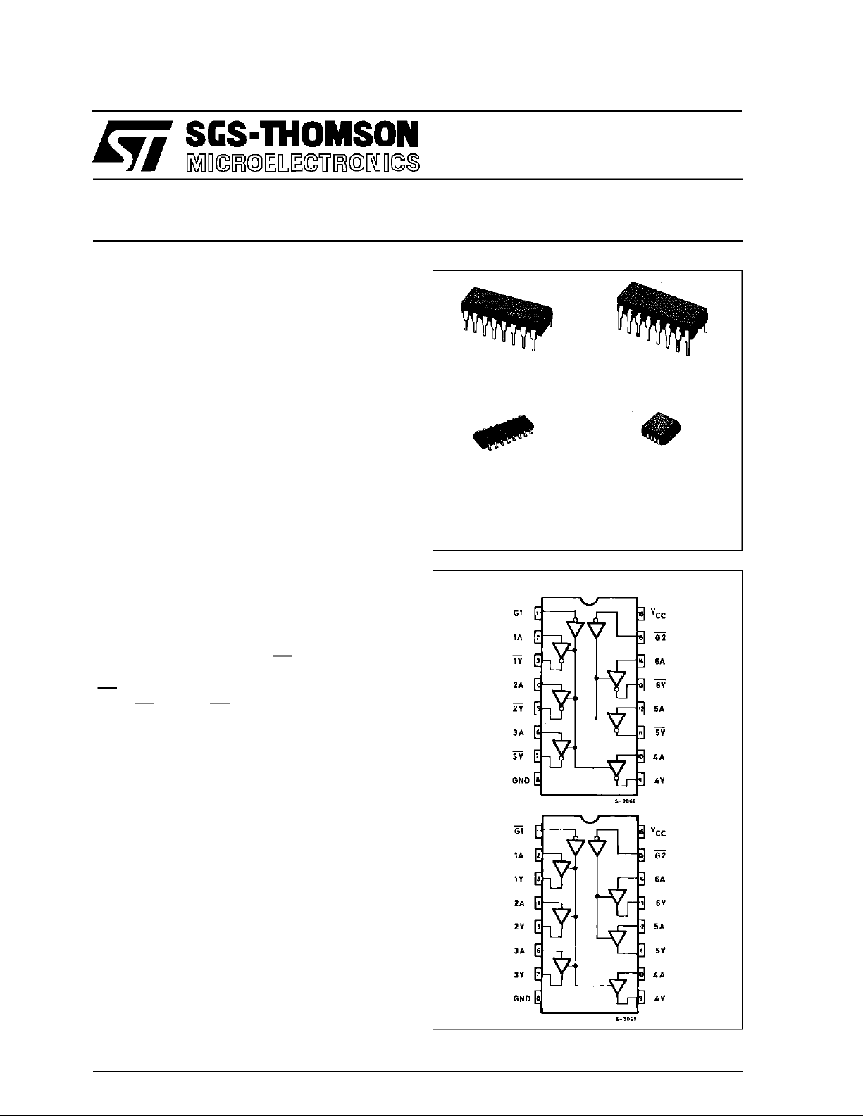
HEX BUS BUFFER(3-STATE)
B1R
(PlasticPackage)
M1R
(MicroPackage)
ORDER CODES :
M54HC TXXX F 1R M74H CTXXXM1R
M74HC TXXX B1R M74HCT XXX C1R
PIN CONNECTIONS(topview)
HCT368
HCT367
F1R
(CeramicPackage)
C1R
(Chip Carrier)
February 1993
1/11
Page 2
M54/M74HCT367/368
INPUT AND OUTPUT EQUIVALENT CIRCUIT
CHIP CARRIER
HCT367 HCT368
TRUTH TABLE
INPUTS OUTPUTS
G An Y n (367) Yn (368)
LLLH
LHHL
HXZZ
X =DON’TCARE Z= HIGHIMPEDANCE
PIN DESCRIPTION (HC T367)
PIN No SYMBOL NAME AND FUNCTION
1, 15 G1, G2 Output Enable Inputs
2, 4, 6, 10,
12, 14
3, 5, 7, 9,
11, 13
8 GND Ground (0V)
16 V
1A to 6A Data Inputs
1Y to 6Y Data Outputs
CC
Positive Supply Voltage
NC = No Internal Connection
PIN DESCRIPTION (HC T368)
PIN No SYMBOL NAME AND FUNCTION
1, 15 G1, G2 Output Enable Inputs
2, 4, 6, 10,
12, 14
3, 5, 7, 9,
11, 13
8 GND Ground (0V)
16 V
1A to 6A Data Inputs
1Y to 6Y Data Outputs
CC
Positive Supply Voltage
2/11
Page 3
M54/M74HCT367/368
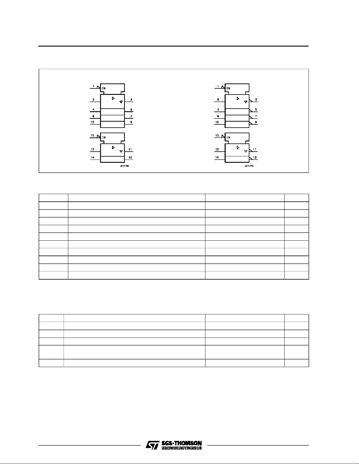
IEC LOGIC SYMBOL
HCT367 HCT368
ABSOLU TE MAXIMU M RAT INGS
Symbol Parameter Value Unit
V
CC
V
V
O
I
IK
I
OK
I
O
or I
I
CC
P
D
T
stg
T
AbsoluteMaximumRatingsarethosevalues beyondwhichdamagetothedevicemayoccur.Functionaloperationunder theseconditionisnotimplied.
(*)500 mW:≅ 65oC derateto 300mW by 10mW/oC: 65oCto85oC
Supply Voltage -0.5 to +7 V
DC Input Voltage -0.5 to VCC+ 0.5 V
I
DC Output Voltage -0.5 to VCC+ 0.5 V
DC Input Diode Current ± 20 mA
DC Output Diode Current ± 20 mA
DC Output Source Sink Current Per Output Pin ± 35 mA
DC VCCor Ground Current ± 70 mA
GND
Power Dissipation 500 (*) mW
Storage Temperature -65 to +150
Lead Temperature (10 sec) 300
L
o
C
o
C
RECO MM ENDED OPERATI N G C O NDI TIONS
Symbol Parameter Value Unit
V
T
t
V
V
r,tf
Supply Voltage 4.5 to 5.5 V
CC
Input Voltage 0 to V
I
Output Voltage 0 to V
O
Operating Temperature: M54HC Series
op
M74HC Series
CC
CC
-55 to +125
-40 to +85
Input Rise and Fall Time (VCC= 4.5 to 5.5V) 0 to 500 ns
RECO MM ENDED OPERATI N G C O NDI TIONS
V
V
o
C
o
C
3/11
Page 4
M54/M74HCT367/368
DC SPECIFICA TIONS
Symbol Parameter
V
V
V
V
I
∆I
High Level Input
IH
Voltage
Low Level Input
IL
Voltage
High Level
OH
Output Voltage
Low Level Output
OL
Voltage
Input Leakage
I
I
Current
Quiescent Supply
CC
Current
Additional worst
CC
case supply
current
Test Conditions Value
V
(V)
4.5
CC
=25oC
A
54HC and 74HC
Min. Typ. Max. Min. Max. Min. Max.
2.0 2.0 2.0 V
-40 to 85oC
74HC
-55 to 125oC
54HC
Unit
T
to
5.5
4.5
0.8 0.8 0.8 V
to
5.5
VI=
IO=-20 µA 4.4 4.5 4.4 4.4
V
IH
4.5
or
I
=-6.0 mA 4.18 4.31 4.13 4.10
O
V
IL
VI=
IO=20µA 0.0 0.1 0.1 0.1
V
IH
4.5
or
I
= 6.0 mA 0.17 0.26 0.33 0.4
O
V
IL
VI=VCCor GND ±0.1 ±1 ±1 µA
5.5
5.5 VI=VCCor GND 4 40 80 µA
5.5 Per Input pin
2.0 2.9 3.0 mA
VI= 0.5V or
V
= 2.4V
I
Other Inputs at
VCCor GND
IO=0
V
V
4/11
Page 5

M54/M74HCT367/368
AC ELECTRICAL CHARACTERISTICS (CL=50pF,Inputtr=tf=6ns)
Test Conditions Value
T
=25oC
Symbol Parameter
t
t
t
t
TLH
THL
PLH
PHL
Output Transition
Time
Propagation
Delay Time
(for HCT367 only)
t
t
PLH
PHL
Propagation
Delay Time
(for HCT368 only)
t
PZL
t
PZH
t
PLZ
t
PHZ
C
C
PD
Output Enable
Time
Output Disable
Time
Input Capacitance 5 10 10 10 pF
IN
(*) Power Dissipation
Capacitance
(*) CPDisdefinedas the valueofthe IC’s internal equivalent capacitance whichiscalculated from theoperatingcurrent consumption withoutload.
(RefertoTest Circuit).Average operting current canbe obtained bythe followingequation. ICC(opr) = CPD•VCC•fIN+ICC/6(per Channel)
V
C
CC
(V)
L
(pF)
2.0 50 7 12 15 18 ns
2.0 50 14 22 28 33
2.0 150 18 28 35 42
2.0 50 15 24 30 36
2.0 150 19 30 38 45
2.0 50 16 25 31 38
2.0 150 20 31 39 47
2.0 50 18 25 31 38 ns
fot HCT367
for HCT368
A
54HC and 74HC
Min. Typ. Max. Min. Max. Min. Max.
47
55
-40 to 85oC
74HC
-55 to 125oC
54HC
Unit
ns
ns
ns
pF
TEST CIRCUIT ICC(Opr.)
* INPUT WAVEFORM IS THE SAME AS THAT IN CASE OF
SWITCHINGCHARACTERISTICSTEST.
CPDCALCULATION
CPDis to be calculated with the following
formula by using the measured value of
ICC(opr.) in the test circuit opposite.
I
(
opr
CPD=
f
CC
IN
)
×
V
CC
In determining the typicalvalue of CPD,a
relatively highfrequency of 1 MHzwasappliedto fIN, in order to eliminate any error
causedby the quiescent supplycurrent.
5/11
Page 6

M54/M74HCT367/368
SWITCHING CHARACTERISTICS TEST WAVEFORM
GND
V
CC
Note: Such a logiclevel shall be appliedto each input thatthe outputvoltagestays in the apposite side to theswitch connection level,when
the output is enabled.
6/11
Page 7

M54/M74HCT367/368
Plastic DIP16 (0.25) MECHANICAL DATA
DIM.
MIN. TYP. MAX. MIN. TYP. MAX.
a1 0.51 0.020
B 0.77 1.65 0.030 0.065
b 0.5 0.020
b1 0.25 0.010
D 20 0.787
E 8.5 0.335
e 2.54 0.100
e3 17.78 0.700
F 7.1 0.280
I 5.1 0.201
L 3.3 0.130
Z 1.27 0.050
mm inch
P001C
7/11
Page 8

M54/M74HCT367/368
Ceramic DIP16/1 MECHANICAL DATA
DIM.
MIN. TYP. MAX. MIN. TYP. MAX.
A 20 0.787
B 7 0.276
D 3.3 0.130
E 0.38 0.015
e3 17.78 0.700
F 2.29 2.79 0.090 0.110
G 0.4 0.55 0.016 0.022
H 1.17 1.52 0.046 0.060
L 0.22 0.31 0.009 0.012
M 0.51 1.27 0.020 0.050
N 10.3 0.406
P 7.8 8.05 0.307 0.317
Q 5.08 0.200
mm inch
8/11
P053D
Page 9

SO16 (Narrow) MECHANICAL DATA
M54/M74HCT367/368
DIM.
MIN. TYP. MAX. MIN. TYP. MAX.
A 1.75 0.068
a1 0.1 0.2 0.004 0.007
a2 1.65 0.064
b 0.35 0.46 0.013 0.018
b1 0.19 0.25 0.007 0.010
C 0.5 0.019
c1 45° (typ.)
D 9.8 10 0.385 0.393
E 5.8 6.2 0.228 0.244
e 1.27 0.050
e3 8.89 0.350
F 3.8 4.0 0.149 0.157
G 4.6 5.3 0.181 0.208
L 0.5 1.27 0.019 0.050
M 0.62 0.024
S8°(max.)
mm inch
P013H
9/11
Page 10

M54/M74HCT367/368
PLCC20 MECHANICAL DATA
DIM.
MIN. TYP. MAX. MIN. TYP. MAX.
A 9.78 10.03 0.385 0.395
B 8.89 9.04 0.350 0.356
D 4.2 4.57 0.165 0.180
d1 2.54 0.100
d2 0.56 0.022
E 7.37 8.38 0.290 0.330
e 1.27 0.050
e3 5.08 0.200
F 0.38 0.015
G 0.101 0.004
M 1.27 0.050
M1 1.14 0.045
mm inch
10/11
P027A
Page 11

M54/M74HCT367/368
Information furnished is believed to be accurate and reliable.However, SGS-THOMSON Microelectronicsassumes no responsability for the
consequences of useof such information nor forany infringement of patents orother rights of third parties which may results from itsuse.No
license isgranted byimplication or otherwiseunder any patentor patentrights ofSGS-THOMSONMicroelectronics. Specificationsmentioned
in this publication aresubject to changewithout notice. This publicationsupersedesand replaces all information previouslysupplied.
SGS-THOMSON Microelectronicsproducts arenot authorizedforuse ascritical componentsinlife supportdevices orsystemswithoutexpress
written approvalof SGS-THOMSON Microelectonics.
1994 SGS-THOMSON Microelectronics- All RightsReserved
Australia - Brazil - France- Germany- HongKong - Italy - Japan - Korea - Malaysia -Malta -Morocco - The Netherlands -
Singapore - Spain - Sweden- Switzerland - Taiwan - Thailand - UnitedKingdom - U.S.A
SGS-THOMSON MicroelectronicsGROUP OF COMPANIES
11/11
 Loading...