

Page 1
.HIGH SPEED
tPD= 9 ns (TYP.)AT VCC=5V
.LOWPOWER DISSIPATION
ICC=1µA(MAX.) AT TA=25°C
.COMPATIBLE WITH TTL OUTPUTS
VIH= 2V(MIN.) VIL= 0.8V (MAX)
.OUTPUT DRIVE CAPABILITY
10 LSTTLLOADS
.SYMMETRICALOUTPUT IMPEDANCE
IOH =IOL= 4 mA (MIN.)
.BALANCEDPROPAGATION DELAYS
t
PLH=tPHL
.PIN AND FUNCTION COMPATIBLE WITH
54/74LS27
DESCRIPTION
The M54/74HCT27 is ahigh speed CMOS TRIPLE
3-INPUT NOR GATE fabricated in silicon gate
C2MOS technology.
It has the same high speed performance of LSTTL
combined with true CMOSlow power consumption.
The internal circuitis composedof 3stages includingbufferedoutput,whichgiveshighnoiseimmunity
anda stableoutput.Allinputsareequippedwith protectioncircuitsagainststaticdischarge andtransient
excessvoltage.Thisintegratedcircuit hasinputand
outputcharacteristics that are fully compatible with
54/74 LSTTL logic families. M54/74HCT devices
are designed to directly interface HSC2MOS systems with TTL and NMOS components. They are
also plugin replacements for LSTTL devicesgiving
a reduction of power consumption.
M54HCT27
M74HCT27
TRIPLE3-INPUT NOR GATE
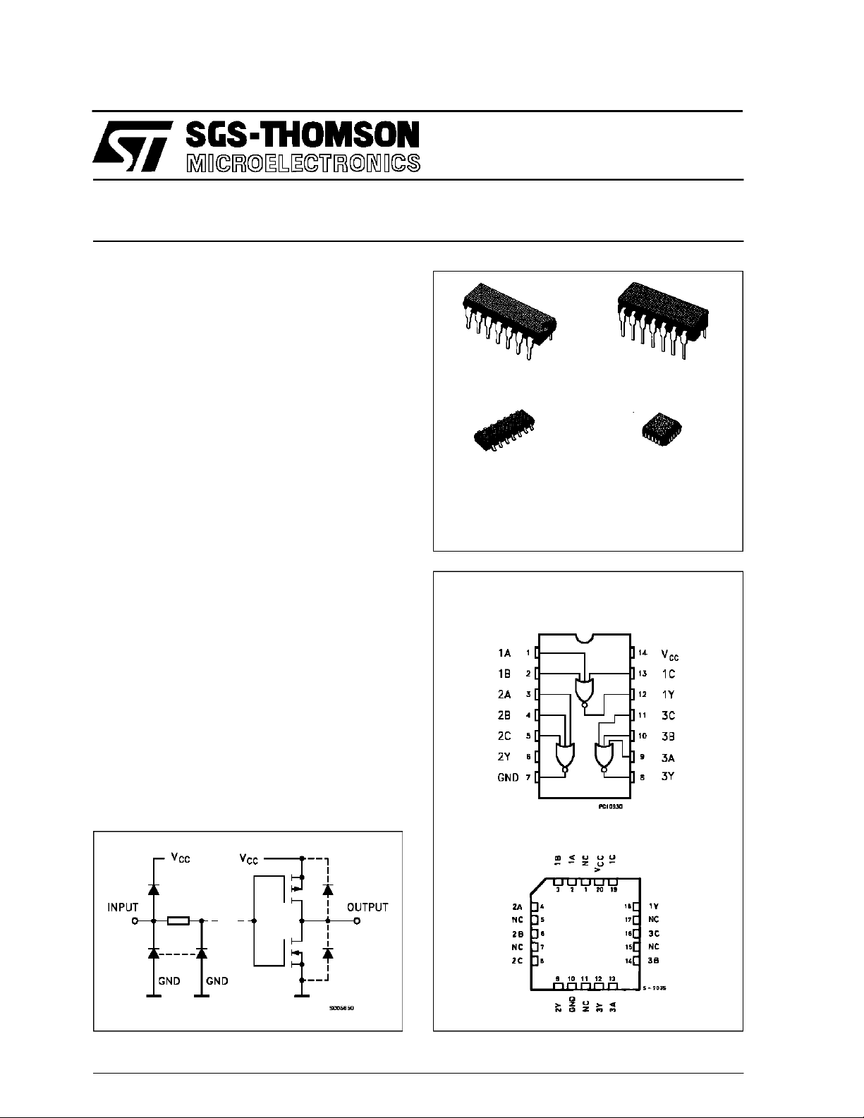
B1R
(PlasticPackage)
M1R
(MicroPackage)
ORDER CODES :
M54HC T27F1R M74H CT27M1R
M74HC T27B1R M74HCT27C1R
PIN CONNECTIONS (top view)
F1R
(CeramicPackage)
C1R
(Chip Carrier)
INPUT AND OUTPUT EQUIVALENT CIRCUIT
February 1993
NC =
No Internal
Connection
1/9
Page 2
M54/M74HCT27
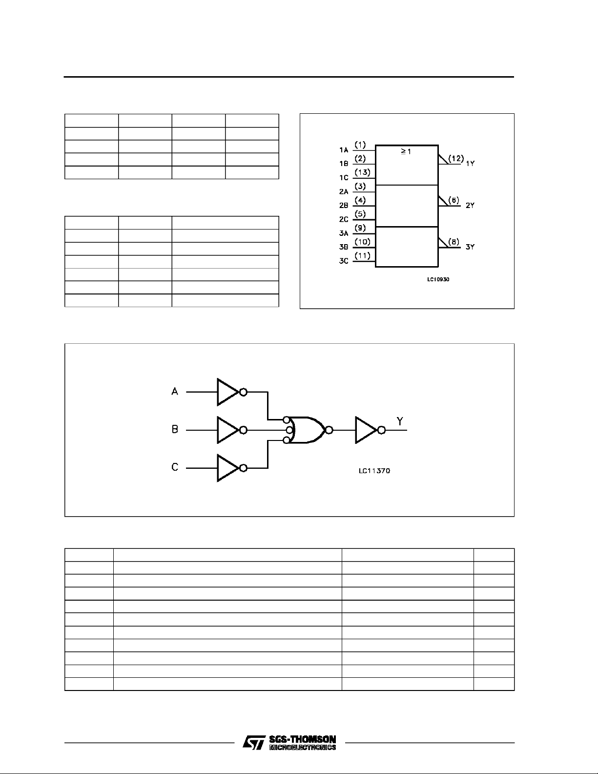
TRUTH TABLE
ABCY
LLLH
HXXL
XHXL
XXHL
PIN DESCRIPTION
PIN No SYMBOL NAME AND FUNCTION
1, 3, 9 1A to 3A Data Inputs
2, 4, 10 1B to 3B Data Inputs
13, 5, 11 1C to 3C Data Inputs
12, 6, 8 1Y to 3Y Data Outputs
7 GND Ground (0V)
14 V
CC
Positive Supply Voltage
LOGI C DIAG RAM
IEC Logic Symbol
ABSOLU TE MAXIMU M RATING S
Symbol Parameter Value Unit
V
CC
V
V
O
I
IK
I
OK
I
O
or I
I
CC
P
D
T
stg
T
L
AbsoluteMaximumRatingsarethosevalues beyond whichdamagetothedevicemayoccur.Functionaloperationunder these conditionisnotimplied.
(*)500 mW:≅ 65oC derateto300mWby 10mW/oC: 65oCto85oC
2/9
Supply Voltage -0.5 to +7 V
DC Input Voltage -0.5 to VCC+ 0.5 V
I
DC Output Voltage -0.5 to VCC+ 0.5 V
DC Input Diode Current ± 20 mA
DC Output Diode Current ± 20 mA
DC Output Source Sink Current Per Output Pin ± 25 mA
DC VCCor Ground Current ± 50 mA
GND
Power Dissipation 500 (*) mW
Storage Temperature -65 to +150
Lead Temperature (10 sec) 300
o
C
o
C
Page 3
M54/M74HCT27
RECO MM ENDED O PERAT IN G C ONDITI ONS
Symbol Parameter Value Unit
V
V
V
T
t
r,tf
DC SPECIFICA TIONS
Symbol Parameter
V
V
V
OH
V
OL
I
I
CC
∆I
Supply Voltage 4.5 to 5.5 V
CC
Input Voltage 0 to V
I
Output Voltage 0 to V
O
Operating Temperature: M54HC Series
op
M74HC Series
CC
CC
-55 to +125
-40 to +85
Input Rise and Fall Time (VCC= 4.5 to 5.5V) 0 to 500 ns
Test Conditions Value
T
High Level Input
IH
Voltage
V
(V)
4.5
=25oC
CC
A
54HC and 74HC
Min. Typ. Max. Min. Max. Min. Max.
2.0 2.0 2.0 V
to
-40 to 85oC
74HC
-55 to 125oC
5.5
Low Level Input
IL
Voltage
4.5
to
0.8 0.8 0.8 V
5.5
High Level
Output Voltage
Low Level Output
Voltage
Input Leakage
I
Current
Quiescent Supply
VI=
IO=-20 µA 4.4 4.5 4.4 4.4
V
IH
4.5
or
I
=-4.0 mA 4.18 4.31 4.13 4.10
O
V
IL
VI=
IO=20µA 0.0 0.1 0.1 0.1
V
IH
4.5
or
I
= 4.0 mA 0.17 0.26 0.33 0.4
O
V
IL
VI=VCCor GND ±0.1 ±1 ±1 µA
5.5
5.5 VI=VCCor GND 1 10 20 µA
Current
Additional worst
CC
case supply
current
5.5 Per Input pin
V
= 0.5V or
I
VI= 2.4V
2.0 2.9 3.0 mA
Other Inputs at
VCCor GND
IO=0
54HC
V
V
o
C
o
C
Unit
V
V
3/9
Page 4

M54/M74HCT27
AC ELECTRICAL CHARACTERISTICS (CL=50pF,Inputtr=tf=6ns)
Test Conditions Value
T
=25oC
Symbol Parameter
t
TLH
t
THL
t
PLH
t
PHL
C
C
PD
Output Transition
Time
Propagation
Delay Time
Input Capacitance 5 10 10 10 pF
IN
(*) Power Dissipation
V
CC
(V)
4.5 8151922
4.5 12 19 24 29
A
54HC and 74HC
Min. Typ. Max. Min. Max. Min. Max.
48
Capacitance
(*) CPDisdefined as the valueofthe IC’s internal equivalent capacitance whichis calculated fromthe operating current consumption withoutload.
(RefertoTest Circuit).Average operting current can be obtained bythefollowingequation. ICC(opr) = CPD•VCC•fIN+ICC/3(per Gate)
SWITCHING CHARACTERISTICS TEST CIRCUIT
-40 to 85oC
74HC
-55 to 125oC
54HC
Unit
ns
ns
pF
TEST CIRCUIT ICC(Opr.)
INPUTWAVEFORMISTHESAVE ASTHATIN CASEOFSWITCHINGCHARACTERISTICSTEST.
4/9
Page 5

Plastic DIP14 MECHANICAL DATA
M54/M74HCT27
DIM.
MIN. TYP. MAX. MIN. TYP. MAX.
a1 0.51 0.020
B 1.39 1.65 0.055 0.065
b 0.5 0.020
b1 0.25 0.010
D 20 0.787
E 8.5 0.335
e 2.54 0.100
e3 15.24 0.600
F 7.1 0.280
I 5.1 0.201
L 3.3 0.130
Z 1.27 2.54 0.050 0.100
mm inch
P001A
5/9
Page 6

M54/M74HCT27
Ceramic DIP14/1 MECHANICAL DATA
DIM.
MIN. TYP. MAX. MIN. TYP. MAX.
A 20 0.787
B 7.0 0.276
D 3.3 0.130
E 0.38 0.015
e3 15.24 0.600
F 2.29 2.79 0.090 0.110
G 0.4 0.55 0.016 0.022
H 1.17 1.52 0.046 0.060
L 0.22 0.31 0.009 0.012
M 1.52 2.54 0.060 0.100
N 10.3 0.406
P 7.8 8.05 0.307 0.317
Q 5.08 0.200
mm inch
6/9
P053C
Page 7

SO14 MECHANICAL DATA
M54/M74HCT27
DIM.
MIN. TYP. MAX. MIN. TYP. MAX.
A 1.75 0.068
a1 0.1 0.2 0.003 0.007
a2 1.65 0.064
b 0.35 0.46 0.013 0.018
b1 0.19 0.25 0.007 0.010
C 0.5 0.019
c1 45° (typ.)
D 8.55 8.75 0.336 0.344
E 5.8 6.2 0.228 0.244
e 1.27 0.050
e3 7.62 0.300
F 3.8 4.0 0.149 0.157
G 4.6 5.3 0.181 0.208
L 0.5 1.27 0.019 0.050
M 0.68 0.026
S8°(max.)
mm inch
P013G
7/9
Page 8

M54/M74HCT27
PLCC20 MECHANICAL DATA
DIM.
MIN. TYP. MAX. MIN. TYP. MAX.
A 9.78 10.03 0.385 0.395
B 8.89 9.04 0.350 0.356
D 4.2 4.57 0.165 0.180
d1 2.54 0.100
d2 0.56 0.022
E 7.37 8.38 0.290 0.330
e 1.27 0.050
e3 5.08 0.200
F 0.38 0.015
G 0.101 0.004
M 1.27 0.050
M1 1.14 0.045
mm inch
8/9
P027A
Page 9

M54/M74HCT27
Information furnished is believed to be accurate and reliable. However, SGS-THOMSON Microelectronics assumes no responsability for the
consequences of use of such information nor for any infringement of patents or other rights of third parties which may results from its use. No
license is granted byimplication or otherwise under any patent or patentrights of SGS-THOMSON Microelectronics. Specificationsmentioned
in this publication are subject to change without notice. This publication supersedes and replaces all information previously supplied.
SGS-THOMSON Microelectronicsproductsarenotauthorizedforuse ascriticalcomponentsinlifesupportdevicesorsystemswithoutexpress
written approval of SGS-THOMSON Microelectonics.
1994 SGS-THOMSON Microelectronics - All Rights Reserved
Australia - Brazil - France - Germany - Hong Kong - Italy - Japan - Korea - Malaysia - Malta - Morocco - The Netherlands -
Singapore -Spain - Sweden- Switzerland -Taiwan - Thailand - UnitedKingdom - U.S.A
SGS-THOMSON Microelectronics GROUP OF COMPANIES
9/9
 Loading...