

Page 1
M54/M74HCT257
M54/M74HCT258
HCT257 QUAD 2 CHANNEL MULTIPLEXER (3-STATE)
HCT258 QUAD 2 CHANNEL MULTIPLEXER (3-STATE,INVERTING)
.HIGH SPEED
tPD= 16 ns(TYP.) at VCC=5V
.LOWPOWER DISSIPATION
ICC=4µA(MAX.) atTA=25°C
.COMPATIBLE WITH TTL OUTPUTS
VIH= 2V(MIN.)VIL= 0.8V (MAX)
.OUTPUTDRIVECAPABILITY
15 LSTTLLOADS
B1R
(PlasticPackage)
F1R
(CeramicPackage)
.SYMMETRICALOUTPUT IMPEDANCE
IOH =IOL= 6 mA (MIN.)
.BALANCEDPROPAGATIONDELAYS
t
PLH=tPHL
.PIN AND FUNCTION COMPATIBLE
WITH 54/74LS257/258
M1R
(MicroPackage)
ORDER CODES :
M54HC TXXX F 1R M74H CTXXXM1R
M74HC TXXX B1R M74HCT XXX C1R
C1R
(Chip Carrier)
DESCRIPTION
The M54/74HCT257 and the M54/74HCT258 are
highspeed CMOSMULTIPLEXERsfabricated with
silicongate C2MOS technology.
They have the same high speed performance of
LSTTL combined with true CMOS low power consumption.
These IC’s are composed of an independent 2channelmultiplexer withcommonSELECT andENABLE INPUT.
The M54/74HCT258 is an inverting multiplexer
while the M54/74HCT257 is a non-inverting multiplexer. When the ENABLE INPUT is held ”High”,
outputs of both IC’sbecome high-impedance state.
IfSELECTINPUTisheld”Low”,”A”dataisselected,
when SELECT INPUT is high ”H”, ”B” data is
chosen.
All inputs are equipped with protection circuits
against static discharge and transient excess voltage.
This integrated circuit has input and output characteristicsthat are fully compatible with 54/74 LSTTL
logic families. M54/74HCT devices are designed to
directly interface HSC2MOSsystems with TTLand
NMOS components. They are also plug in replace-
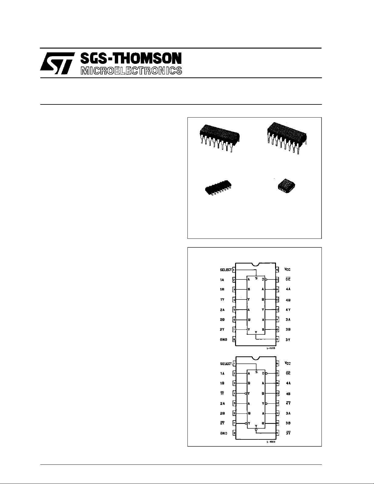
PIN CONNECTIONS(topview)
HCT257
HCT258
February 1993
1/12
Page 2
M54/M74HCT257/258
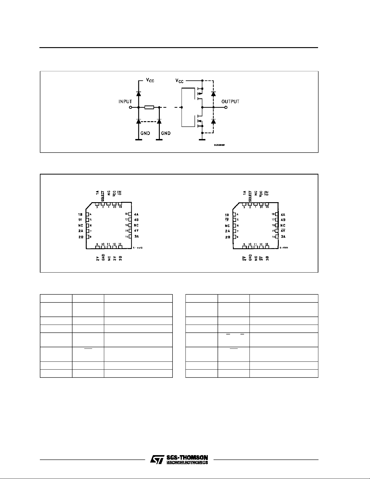
INPUT AND OUTPUT EQUIVALENT CIRCUIT
CHIP CARRIER
HCT257 HCT258
NC = No Internal Connection
PIN DESCRIPTION ( HCT 257)
PIN No SYMBOL NAME AND FUNCTION
1 SELECT Common Data Select
Input
2, 5, 14, 11 1A to 4A Data Input From Source A
3, 6, 13, 10 1B to 4B Data Inputs from Source B
4, 7, 12, 9 1Y to 4Y 3 State Multiplexer
Outputs
15 OE 3 State Output Enable
Inputs (Active LOW)
8 GND Ground (0V)
16 V
CC
Positive Supply Voltage
PIN DESCRIPTION (HCT258)
PIN No SYMBOL NAME AND FUNCTION
1 SELECT Common Data Select
Input
2, 5, 14, 11 1A to 4A Data Input From Source A
3, 6, 13, 10 1B to 4B Data Inputs from Source B
4, 7, 12, 9 1Y to 4Y 3 State Multiplexer
Outputs
15 OE 3 State Output Enable
Inputs (Active LOW)
8 GND Ground (0V)
16 V
CC
Positive Supply Voltage
2/12
Page 3
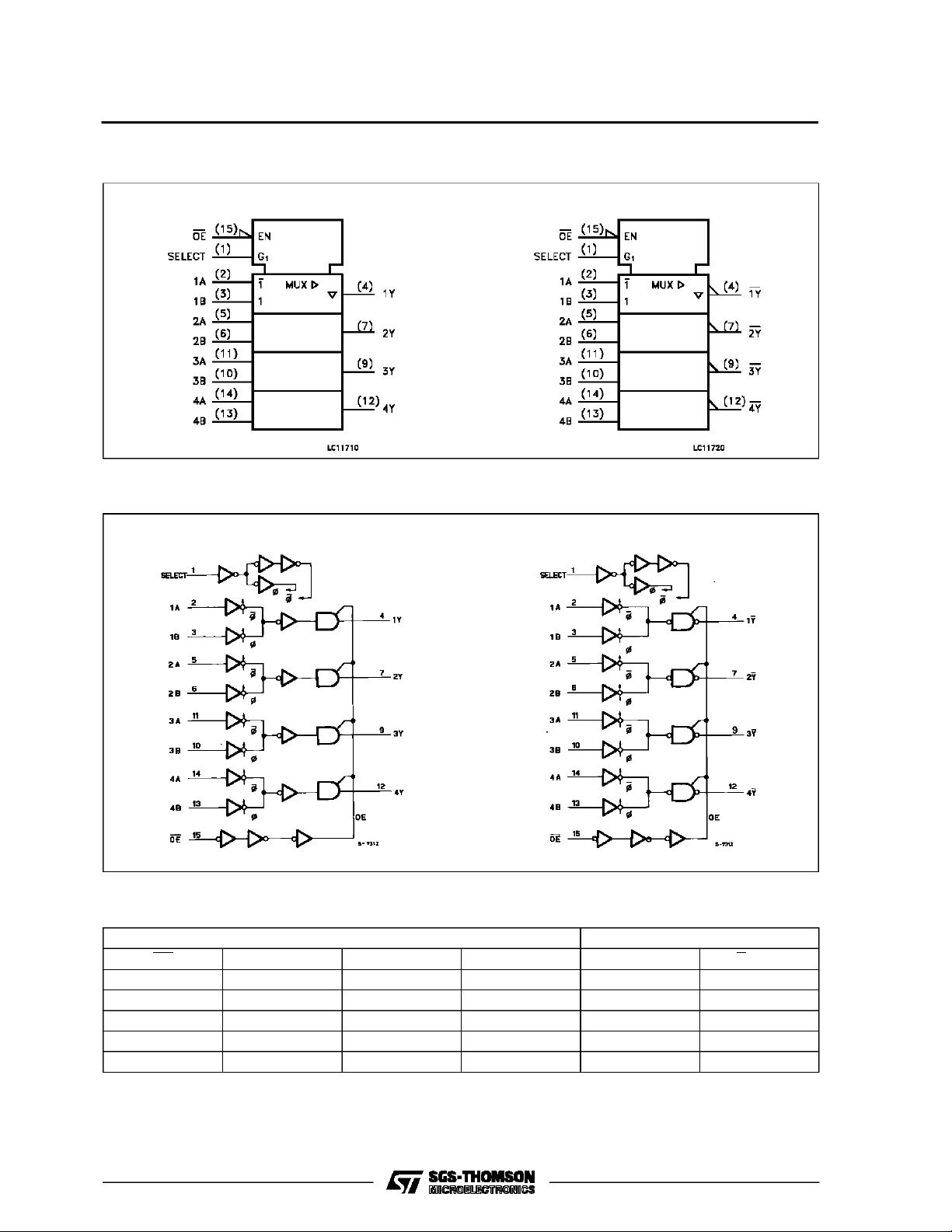
IEC LOGIC SYMBOL
LOGIC DIAGRAM
M54/M74HCT257/258
HCT258HCT257
HCT257 HCT258
TRUTH TABLE
OE SELECT A B Y (257) Y (258)
HXXXZZ
LLLXLH
LLHXHL
LHXLLH
LHXHHL
X =DON’TCARE Z = HIGHIMPEDANCE
INPUTS OUTPUTS
3/12
Page 4
M54/M74HCT257/258
ABSOLU TE MAXIMU M RAT I NG S
Symbol Parameter Value Unit
V
CC
V
V
O
I
IK
I
OK
I
O
I
or I
CC
P
D
T
stg
T
AbsoluteMaximumRatingsarethosevalues beyondwhichdamagetothedevicemayoccur.Functionaloperationunder theseconditionisnotimplied.
(*)500 mW:≅ 65oC derateto 300mW by 10mW/oC: 65oCto85oC
RECO MM ENDED OPERATIN G CONDI TI O NS
Symbol Parameter Value Unit
V
CC
V
I
V
O
T
op
t
r,tf
Supply Voltage -0.5 to +7 V
DC Input Voltage -0.5 to VCC+ 0.5 V
I
DC Output Voltage -0.5 to VCC+ 0.5 V
DC Input Diode Current ± 20 mA
DC Output Diode Current ± 20 mA
DC Output Source Sink Current Per Output Pin ± 35 mA
DC VCCor Ground Current ± 70 mA
GND
Power Dissipation 500 (*) mW
Storage Temperature -65 to +150
Lead Temperature (10 sec) 300
L
Supply Voltage 4.5 to 5.5 V
Input Voltage 0 to V
Output Voltage 0 to V
Operating Temperature: M54HC Series
M74HC Series
CC
CC
-55 to +125
-40 to +85
Input Rise and Fall Time (VCC= 4.5 to 5.5V) 0 to 500 ns
o
C
o
C
V
V
o
C
o
C
4/12
Page 5

DC SPECIFICATIO NS
Symbol Parameter
V
V
V
V
I
I
∆I
High Level Input
IH
Voltage
Low Level Input
IL
Voltage
High Level
OH
Output Voltage
Low Level Output
OL
Voltage
3-State Output
OZ
Off State Current
I
Input Leakage
I
Current
Quiescent Supply
CC
Current
Additional worst
CC
case supply
current
M54/M74HCT257/258
Test Conditions Value
T
=25oC
V
(V)
4.5
CC
A
54HC and 74HC
Min. Typ. Max. Min. Max. Min. Max.
2.0 2.0 2.0 V
to
5.5
4.5
to
5.5
VI=
IO=-20 µA 4.4 4.5 4.4 4.4
V
IH
4.5
or
I
=-4.0 mA 4.18 4.31 4.13 4.10
O
V
IL
V
=
IO=20µA 0.0 0.1 0.1 0.1
I
V
IH
4.5
or
I
= 4.0 mA 0.17 0.26 0.33 0.4
O
V
IL
5.5 VI=VCCor GND ±0.5 ±5 ±10 µA
5.5 VI=VCCor GND ±0.1 ±1 ±1 µA
5.5 VI=VCCor GND 1 10 20 µA
5.5 Per Input pin
VI= 0.5V or
VI= 2.4V
Other Inputs at
VCCor GND
-40 to 85oC
74HC
-55 to 125oC
54HC
Unit
0.8 0.8 0.8 V
2.0 2.9 3.0 mA
V
V
5/12
Page 6

M54/M74HCT257/258
AC ELECTRICAL CHARACTERISTICS (CL=50pF,Inputtr=tf=6ns)
Test Conditions Value
T
=25oC
Symbol Parameter
t
TLH
t
THL
t
PLH
t
PHL
Output Transition
Time
Propagation
Delay Time
(A, B - Y)
t
t
PLH
PHL
Propagation
Delay Time
V
CC
(V)
4.5 7121518ns
4.5
HCT257
HCT258 17 27 34 41
4.5 20 30 38 45 ns
A
54HC and 74HC
Min. Typ. Max. Min. Max. Min. Max.
19 30 38 45 ns
(SELECT - Y)
t
PZL
t
PZH
t
PLZ
t
PHZ
C
C
Output Enable
Time
Output Disable
Time
Input Capacitance 5 10 10 10 pF
IN
Output
OUT
4.5 RL=1KΩ 18 30 38 45 ns
4.5 RL=1KΩ 16 30 38 45 ns
10
Capacitance
C
(*) Power Dissipation
PD
Capacitance
(*) CPDisdefinedas the value ofthe IC’s internal equivalent capacitance which is calculated fromthe operating current consumption withoutload.
(RefertoTest Circuit).Average operting current canbe obtainedby thefollowingequation. ICC(opr) = CPD•VCC•fIN+ICC/4(per Channel)
HCT257
HCT258
34
33
-40 to 85oC
74HC
-55 to 125oC
54HC
Unit
pF
pF
6/12
Page 7

SWITCHING CHARACTERISTICS TEST WAVEFORM
M54/M74HCT257/258
TEST CIRCUIT ICC(Opr.)
INPUT WAVEFORM IS THE SAME AS THAT IN CASE OF
SWITCHINGCHARACTERSISTICSTESt.
CPDCALCULATION
CPDis to be calculated with the following
formula by using the measured value of
ICC (opr.) in the test circuit opposite.
I
(
opr
CPD=
f
CC
IN
)
×
V
CC
7/12
Page 8

M54/M74HCT257/258
Plastic DIP16 (0.25) MECHANICAL DATA
DIM.
MIN. TYP. MAX. MIN. TYP. MAX.
a1 0.51 0.020
B 0.77 1.65 0.030 0.065
b 0.5 0.020
b1 0.25 0.010
D 20 0.787
E 8.5 0.335
e 2.54 0.100
e3 17.78 0.700
F 7.1 0.280
I 5.1 0.201
L 3.3 0.130
Z 1.27 0.050
mm inch
8/12
P001C
Page 9

Ceramic DIP16/1 MECHANICAL DATA
M54/M74HCT257/258
DIM.
MIN. TYP. MAX. MIN. TYP. MAX.
A 20 0.787
B 7 0.276
D 3.3 0.130
E 0.38 0.015
e3 17.78 0.700
F 2.29 2.79 0.090 0.110
G 0.4 0.55 0.016 0.022
H 1.17 1.52 0.046 0.060
L 0.22 0.31 0.009 0.012
M 0.51 1.27 0.020 0.050
N 10.3 0.406
P 7.8 8.05 0.307 0.317
Q 5.08 0.200
mm inch
P053D
9/12
Page 10

M54/M74HCT257/258
SO16 (Narrow) MECHANICAL DATA
DIM.
MIN. TYP. MAX. MIN. TYP. MAX.
A 1.75 0.068
a1 0.1 0.2 0.004 0.007
a2 1.65 0.064
b 0.35 0.46 0.013 0.018
b1 0.19 0.25 0.007 0.010
C 0.5 0.019
c1 45° (typ.)
D 9.8 10 0.385 0.393
E 5.8 6.2 0.228 0.244
e 1.27 0.050
e3 8.89 0.350
F 3.8 4.0 0.149 0.157
G 4.6 5.3 0.181 0.208
L 0.5 1.27 0.019 0.050
M 0.62 0.024
S8°(max.)
mm inch
10/12
P013H
Page 11

PLCC20 MECHANICAL DATA
M54/M74HCT257/258
DIM.
MIN. TYP. MAX. MIN. TYP. MAX.
A 9.78 10.03 0.385 0.395
B 8.89 9.04 0.350 0.356
D 4.2 4.57 0.165 0.180
d1 2.54 0.100
d2 0.56 0.022
E 7.37 8.38 0.290 0.330
e 1.27 0.050
e3 5.08 0.200
F 0.38 0.015
G 0.101 0.004
M 1.27 0.050
M1 1.14 0.045
mm inch
P027A
11/12
Page 12

M54/M74HCT257/258
Information furnished is believed to be accurate and reliable.However, SGS-THOMSONMicroelectronics assumes no responsability for the
consequences of useof such information nor forany infringement of patents orother rights of third parties which may results from itsuse. No
license isgranted byimplication or otherwiseunder any patentor patentrights ofSGS-THOMSONMicroelectronics. Specificationsmentioned
in this publication aresubject to changewithout notice. Thispublication supersedes and replaces all informationpreviouslysupplied.
SGS-THOMSON Microelectronicsproducts arenot authorizedforuse ascritical componentsinlife supportdevices orsystemswithoutexpress
written approvalof SGS-THOMSON Microelectonics.
1994 SGS-THOMSON Microelectronics- All RightsReserved
Australia - Brazil - France- Germany- HongKong - Italy - Japan - Korea - Malaysia- Malta - Morocco - The Netherlands -
Singapore - Spain - Sweden- Switzerland - Taiwan - Thailand - UnitedKingdom - U.S.A
SGS-THOMSON MicroelectronicsGROUP OF COMPANIES
12/12
 Loading...