

Page 1
OCTAL BUS BUFFERWITH3 STATE OUTPUTS
HCT24 0: INVERTED-H CT241 /244 NON INVER TED
.HIGH SPEED
tPD= 13 ns(TYP.) at VCC=5V
.LOWPOWER DISSIPATION
ICC=4µA (MAX.) at TA=25oC
.COMPATIBLE WITH TTL OUTPUTS
VIH= 2V (MIN.) VIL= 0.8V (MAX)
.OUTPUT DRIVE CAPABILITY
15 LSTTLLOADS
.SYMMETRICALOUTPUT IMPEDANCE
|IOH|=IOL=6 mA (MIN)
.BALANCEDPROPAGATION DELAYS
t
PLH=tPHL
.PIN AND FUNCTION COMPATIBLE
WITH 54/74LS240/241/244
DESCRIPTION
M54HCT240/241/244
M74HCT240/241/244
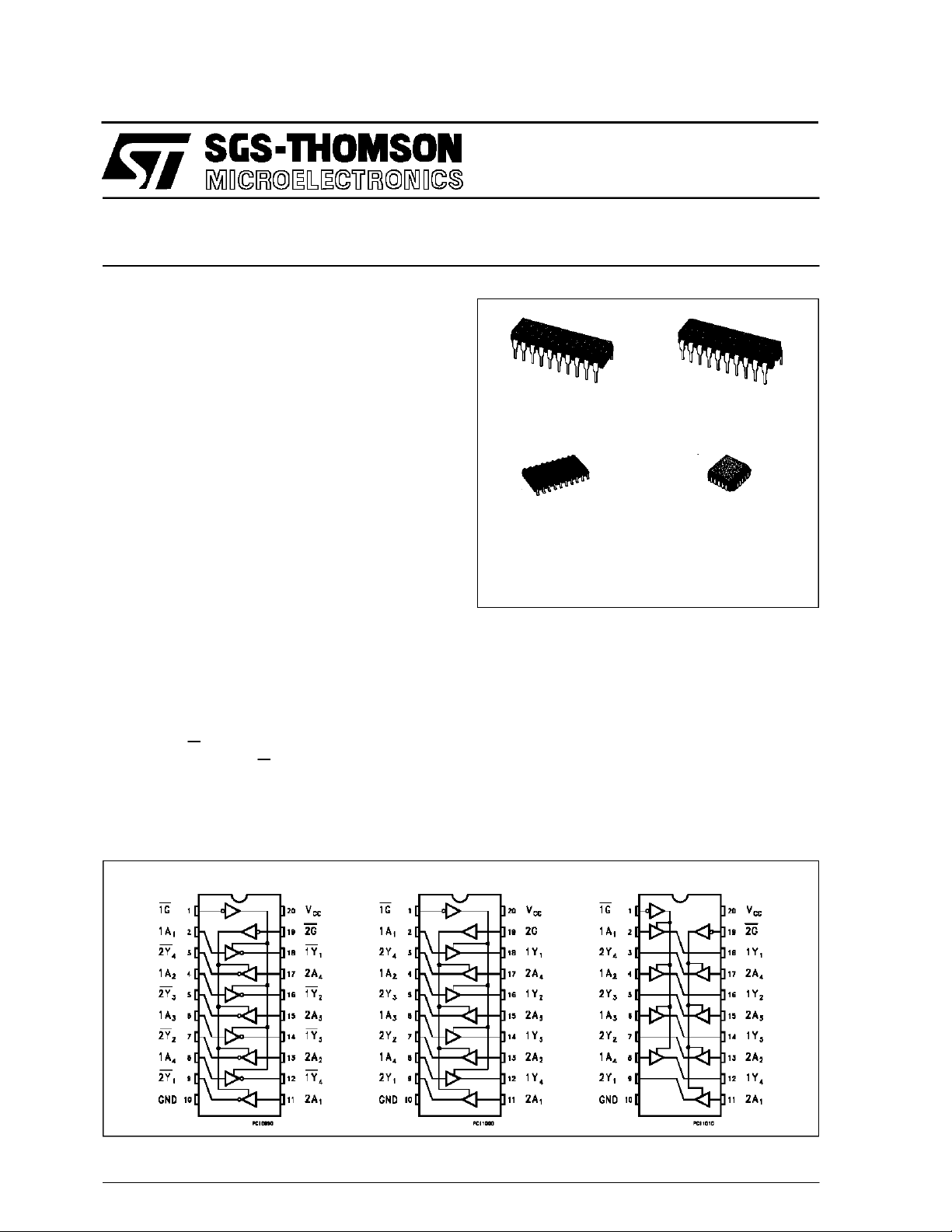
B1R
(PlasticPackage)
M1R
(MicroPackage)
ORDER CODES :
M54HC TXXXF 1R M74HCTXXXM1R
M74HC TXXXB1R M74HCTXXX C1R
F1R
(CeramicPackage)
C1R
(Chip Carrier)
The M54/74HCT240, HCT241 and HCT244 are
high speed CMOS OCTAL BUS BUFFERs
fabricated in silicongate C2MOS technology.
They have the same high speed performance of
LSTTL combined with true CMOS low power
consumption. The designer has a choise of select
combination ofinverting and non-inverting outputs,
symmetrical G (active lowoutputcontrol) input, and
complementary G and G inputs. Each controlinput
governs four BUS BUFFERs.
This integrated circuit has input and output
PIN CONNECTION (top view)
characteristics that are fully compatible with 54/74
LSTTL logic families. M54/74HCT devices are
designed to directly interface HSC2MOS systems
with TTL and NMOS components.
They are also plug in replacements for LSTTL
devices giving a reduction of power consumption.
Thesedevicesaredesigned to be used with3 state
memory address drivers, etc.
All inputs are equipped with protection circuits
against static discharge and transient excess
voltage.
HCT244HCT241HCT240
September 1993
1/12
Page 2
M54/M74HCT240/241/244
CHIP CARRIER
HCT244HCT241HCT240
INPUT AND OUTPUT EQUIVALENT CIRCUIT PIN DESCRIPTION (HC T240)
PIN No SYMBOL NAME AND FUNCTION
1 1G Output Enable Input
2, 4, 6, 8 1A1 to 1A4 Data Inputs
9, 7, 5, 3 2Y1 to 2Y4 Data Outputs
11, 13, 15,172A1 to 2A4 Data Inputs
PIN DESCRIPTION (HCT241)
PIN No SYMBOL NAME AND FUNCTION
1 1G Output Enable Input
2, 4, 6, 8 1A1 to 1A4 Data Inputs
9, 7, 5, 3 2Y1 to 2Y4 Data Outputs
11, 13, 15,172A1 to 2A4 Data Inputs
18, 16, 14,121Y1 to 1Y4 Data Outputs
19 2G Output Enabel Input
10 GND Ground (0V)
20 V
CC
Positive Supply Voltage
18, 16, 14,121Y1 to 1Y4 Data Outputs
19 2G Output Enabel Input
10 GND Ground (0V)
20 V
CC
Positive Supply Voltage
PIN DESCRIPTION (HCT244)
PIN No SYMBOL NAME AND FUNCTION
1 1G Output Enable Input
2, 4, 6, 8 1A1 to 1A4 Data Inputs
9, 7, 5, 3 2Y1 to 2Y4 Data Outputs
11, 13, 15,172A1 to 2A4 Data Inputs
18, 16, 14,121Y1 to 1Y4 Data Outputs
19 2G Output Enabel Input
10 GND Ground (0V)
20 V
CC
Positive Supply Voltage
2/12
Page 3
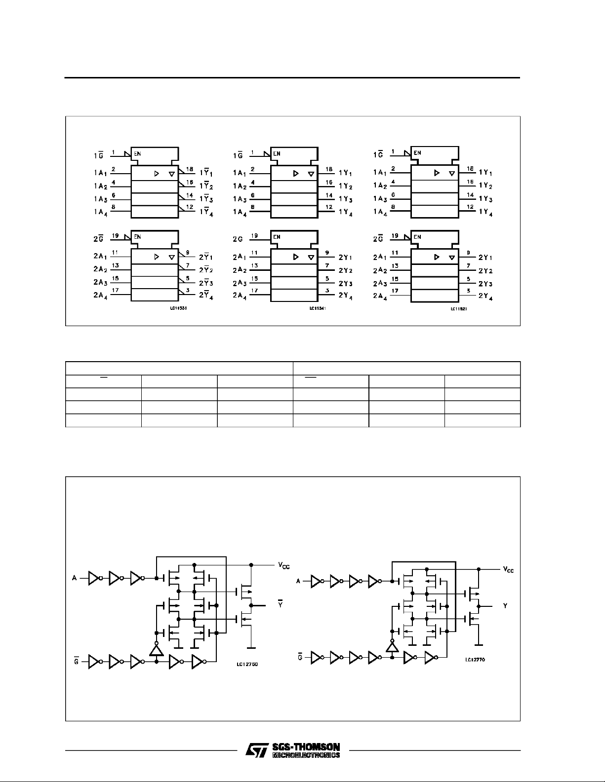
IEC LOGIC SYMBOLS
TRUTH TABLE
M54/M74HCT240/241/244
HCT244HCT241HCT240
INPUT OUTPUT
G G (HCT241) An Yn (HCT240) Yn (HCT241) Yn (HCT244)
LHLHLL
LHHLHH
X: ”H” or ”L”
Z: High impedance
HLXZZZ
CIRCUIT SCHEMATIC (1/8 PACKAGE)
HCT240 HCT241/244
3/12
Page 4
M54/M74HCT240/241/244
ABSOLU TE MAXI MU M RAT INGS
Symbol Parameter Value Unit
V
CC
V
V
O
I
IK
I
OK
I
O
I
or I
CC
P
D
T
stg
T
AbsoluteMaximumRatingsarethosevalues beyondwhichdamageto thedevicemayoccur.Functionaloperationunder thesecondition isnotimplied.
(*)500 mW:≅ 65oC derateto 300 mW by 10mW/oC: 65oCto85oC
RECO MM ENDED OPERAT IN G CO NDI TIONS
Symbol Parameter Value Unit
V
CC
V
I
V
O
T
op
t
r,tf
Supply Voltage -0.5 to +7 V
DC Input Voltage -0.5 to VCC+ 0.5 V
I
DC Output Voltage -0.5 to VCC+ 0.5 V
DC Input Diode Current ± 20 mA
DC Output Diode Current ± 20 mA
DC Output Source Sink Current Per Output Pin ± 35 mA
DC VCCor Ground Current ± 70 mA
GND
Power Dissipation 500 (*) mW
Storage Temperature -65 to +150
Lead Temperature (10 sec) 300
L
Supply Voltage 4.5 to 5.5 V
Input Voltage 0 to V
Output Voltage 0 to V
Operating Temperature: M54HC Series
M74HC Series
CC
CC
-55 to +125
-40 to +85
Input Rise and Fall Time (VCC= 4.5 to 5.5V) 0 to 500 ns
o
C
o
C
V
V
o
C
o
C
4/12
Page 5

DC SPECIFICATIONS
Symbol Parameter
V
V
V
V
I
∆I
High Level Input
IH
Voltage
Low Level Input
IL
Voltage
High Level
OH
Output Voltage
Low Level Output
OL
Voltage
Input Leakage
I
I
Current
Quiescent Supply
CC
Current
Additional worst
CC
case supply
current
M54/M74HCT240/241/244
Test Conditions Value
T
=25oC
V
(V)
4.5
CC
A
54HC and 74HC
Min. Typ. Max. Min. Max. Min. Max.
2.0 2.0 2.0 V
to
5.5
4.5
to
5.5
VI=
IO=-20 µA 4.4 4.5 4.4 4.4
V
IH
4.5
or
I
=-6.0 mA 4.18 4.31 4.13 4.10
O
V
IL
VI=
IO=20µA 0.0 0.1 0.1 0.1
V
IH
4.5
or
I
= 6.0 mA 0.17 0.26 0.33 0.4
O
V
IL
VI=VCCor GND ±0.1 ±1 ±1 µA
5.5
5.5 VI=VCCor GND 4 40 80 µA
5.5 Per Input pin
VI= 0.5V or 2.4V
Other Inputs at
V
or GND
CC
-40 to 85oC
74HC
-55 to 125oC
54HC
Unit
0.8 0.8 0.8 V
2.0 2.9 3.0 mA
V
V
5/12
Page 6

M54/M74HCT240/241/244
AC ELECTRICAL CHARACTERISTICS (CL=50pF,Inputtr=tf=6ns)
Test Conditions Value
T
=25oC
Symbol Parameter
t
TLH
t
THL
t
PLH
t
PHL
t
PLH
t
PHL
t
PZL
t
PZH
t
PLZ
t
PHZ
C
C
Output Transition
Time
Propagation
Delay Time
Propagation
Delay Time
Output Enable
Time
Output Disable
Time
Input Capacitance 5 10 10 10 pF
IN
Output
OUT
V
C
CC
(V)
L
(pF)
4.5 50 7 12 15 18 ns
4.5 50 15 22 28 33 ns
4.5 150 21 30 38 45 ns
4.5 50 15 25 31 38 ns
4.5 150 21 33 41 50 ns
4.5 50 RL=1KΩ 17 30 38 45 ns
4.5 150 R
=1KΩ 23 38 48 57 ns
L
4.5 50 RL=1KΩ 16 30 38 45 ns
A
54HC and 74HC
Min. Typ. Max. Min. Max. Min. Max.
10 pF
Capacitance
(*) Power Dissipation
C
PD
Capacitance
(*) CPDisdefined as the valueof the IC’s internal equivalent capacitance which is calculated fromthe operating current consumption withoutload.
(Referto Test Circuit).Average opertingcurrentcan be obtained bythefollowingequation. ICC(opr) = CPD•VCC•fIN+ICC/8(per circuit)
HCT240
HCT241/244
33
31
-40 to 85oC
74HC
-55 to 125oC
54HC
Unit
pF
TEST CIRCUIT ICC(Opr.)
HCT240
6/12
Page 7

SWITCHING CHARACTERISTICS TEST WAVEFORM
M54/M74HCT240/241/244
7/12
Page 8

M54/M74HCT240/241/244
Plastic DIP20 (0.25) MECHANICAL DATA
DIM.
MIN. TYP. MAX. MIN. TYP. MAX.
a1 0.254 0.010
B 1.39 1.65 0.055 0.065
b 0.45 0.018
b1 0.25 0.010
D 25.4 1.000
E 8.5 0.335
e 2.54 0.100
e3 22.86 0.900
F 7.1 0.280
I 3.93 0.155
L 3.3 0.130
Z 1.34 0.053
mm inch
8/12
P001J
Page 9

M54/M74HCT240/241/244
Ceramic DIP20 MECHANICAL DATA
DIM.
MIN. TYP. MAX. MIN. TYP. MAX.
A 25 0.984
B 7.8 0.307
D 3.3 0.130
E 0.5 1.78 0.020 0.070
e3 22.86 0.900
F 2.29 2.79 0.090 0.110
G 0.4 0.55 0.016 0.022
I 1.27 1.52 0.050 0.060
L 0.22 0.31 0.009 0.012
M 0.51 1.27 0.020 0.050
N1 4° (min.), 15° (max.)
P 7.9 8.13 0.311 0.320
Q 5.71 0.225
mm inch
P057H
9/12
Page 10

M54/M74HCT240/241/244
SO20 MECHANICAL DATA
DIM.
MIN. TYP. MAX. MIN. TYP. MAX.
A 2.65 0.104
a1 0.10 0.20 0.004 0.007
a2 2.45 0.096
b 0.35 0.49 0.013 0.019
b1 0.23 0.32 0.009 0.012
C 0.50 0.020
c1 45° (typ.)
D 12.60 13.00 0.496 0.512
E 10.00 10.65 0.393 0.419
e 1.27 0.050
e3 11.43 0.450
F 7.40 7.60 0.291 0.299
L 0.50 1.27 0.19 0.050
M 0.75 0.029
S8°(max.)
mm inch
10/12
P013L
Page 11

PLCC20 MECHANICAL DATA
M54/M74HCT240/241/244
DIM.
MIN. TYP. MAX. MIN. TYP. MAX.
A 9.78 10.03 0.385 0.395
B 8.89 9.04 0.350 0.356
D 4.2 4.57 0.165 0.180
d1 2.54 0.100
d2 0.56 0.022
E 7.37 8.38 0.290 0.330
e 1.27 0.050
e3 5.08 0.200
F 0.38 0.015
G 0.101 0.004
M 1.27 0.050
M1 1.14 0.045
mm inch
P027A
11/12
Page 12

M54/M74HCT240/241/244
Information furnished is believed to be accurate and reliable. However, SGS-THOMSON Microelectronics assumes no responsability for the
consequences of use of such information nor forany infringementof patents or other rights of third parties which mayresults from its use. No
license is granted byimplication or otherwise under any patent or patent rights of SGS-THOMSON Microelectronics. Specificationsmentioned
in this publication are subject to changewithout notice. This publication supersedes and replaces all information previously supplied.
SGS-THOMSON Microelectronicsproducts are not authorized foruse ascritical componentsin life support devices or systems without express
written approval of SGS-THOMSON Microelectonics.
1994 SGS-THOMSON Microelectronics - All Rights Reserved
Australia - Brazil - France- Germany - HongKong - Italy - Japan - Korea - Malaysia - Malta - Morocco - The Netherlands -
Singapore -Spain - Sweden- Switzerland - Taiwan - Thailand - UnitedKingdom - U.S.A
SGS-THOMSON Microelectronics GROUP OF COMPANIES
12/12
 Loading...