

Page 1

HEX D-TYPE FLIP FLOPWITH CLEAR
.HIGH SPEED
f
= 56 MHz(TYP.) AT VCC=5V
MAX
.LOWPOWER DISSIPATION
ICC=4µA(MAX.) AT TA=25°C
.COMPATIBLE WITH TTL OUTPUTS
VIH= 2V (MIN.) VIL= 0.8V (MAX)
.OUTPUT DRIVE CAPABILITY
10 LSTTLLOADS
.SYMMETRICALOUTPUT IMPEDANCE
IOH =IOL= 4 mA(MIN.)
.BALANCEDPROPAGATION DELAYS
t
PLH=tPHL
.PIN AND FUNCTION COMPATIBLE WITH
54/74LS174
DESCRIPTION
TheM54/74HCT174 is a highspeed CMOSHEXDTYPEFLIP-FLOP WITHCLEARfabricated insilicon
gateC2MOStechnology. Ithasthesamehighspeed
performance of LSTTL combined with true CMOS
low power consumption.
InformationsignalsappliedtoD inputsaretransfered
totheQoutputonthepositivegoingedgeoftheclock
pulse. When the CLEAR inputisheld low,the Qoutputsare held low independently of the otherinputs.
This integrated circuit has input and output characteristics that are fully compatible with 54/74 LSTTL
logic families. M54/74HCT devices are designed to
directly interface HSC2MOS systems with TTL and
NMOScomponents. Theyare also plug in replacements forLSTTL devicesgivingareductionofpower
consumption. Allinputs are equipped withprotection
circuitsagainst staticdischargeandtransientexcess
voltage.
M54HCT174
M74HCT174
B1R
(PlasticPackage)
M1R
(MicroPackage)
ORDER CODES :
M54HC T174F1R M74H CT174M1R
M74HC T174B1R M74HCT174C1R
PIN CONNECTIONS(top view)
F1R
(CeramicPackage)
C1R
(Chip Carrier)
INPUT AND OUTPUT EQUIVALENT CIRCUIT
February 1993
NC =
No Internal
Connection
1/11
Page 2

M54/M74HCT174
TRUTH TABLE
INPUTS OUTPUTS
CLEAR D CK Q
L X X L CLEAR
HL L
HH H
HX Q
X:Don’t Care
PIN DESCRIPTION
PIN No SYMBOL NAME AND FUNCTION
1 CLEAR AsynchronousMaster
Reset (Active LOW)
2, 5, 7, 10,
12, 15
3, 4, 6, 11,
13, 14
9 CLOCK Clock Input (LOW to
8 GND Ground (0V)
16 V
Q0 to Q5 Flip-flop Outputs
D0 to D5 Data Inputs
HIGH, edge triggered)
CC
Positive Supply Voltage
n
IEC LOGIC SYMBOL
FUNCTION
NO CHANGE
LOGI C DIAG RAM
2/11
Page 3

M54/M74HCT174
ABSOLU TE MAXIMU M R AT I NG S
Symbol Parameter Value Unit
V
CC
V
V
O
I
IK
I
OK
I
O
I
or I
CC
P
D
T
stg
T
AbsoluteMaximumRatingsarethosevaluesbeyondwhichdamagetothedevice mayoccur.Functionaloperationunder theseconditionisnotimplied.
(*)500 mW:≅ 65oC derateto 300 mWby 10mW/oC: 65oCto85oC
RECO MM ENDED O PERAT IN G CONDI TIONS
Symbol Parameter Value Unit
V
CC
V
I
V
O
T
op
t
r,tf
Supply Voltage -0.5 to +7 V
DC Input Voltage -0.5 to VCC+ 0.5 V
I
DC Output Voltage -0.5 to VCC+ 0.5 V
DC Input Diode Current ± 20 mA
DC Output Diode Current ± 20 mA
DC Output Source Sink Current Per Output Pin ± 25 mA
DC VCCor Ground Current ± 50 mA
GND
Power Dissipation 500 (*) mW
Storage Temperature -65 to +150
Lead Temperature (10 sec) 300
L
Supply Voltage 4.5 to 5.5 V
Input Voltage 0 to V
Output Voltage 0 to V
Operating Temperature: M54HC Series
M74HC Series
CC
CC
-55 to +125
-40 to +85
Input Rise and Fall Time (VCC= 4.5 to 5.5V) 0 to 500 ns
o
C
o
C
V
V
o
C
o
C
3/11
Page 4
M54/M74HCT174
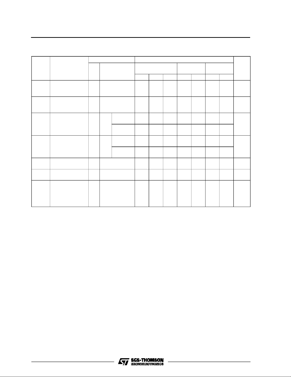
DC SPECIFICATIO NS
Symbol Parameter
V
V
V
V
I
∆I
High Level Input
IH
Voltage
Low Level Input
IL
Voltage
High Level
OH
Output Voltage
Low Level Output
OL
Voltage
Input Leakage
I
I
Current
Quiescent Supply
CC
Current
Additional worst
CC
case supply
current
Test Conditions Value
V
(V)
4.5
CC
=25oC
A
54HC and 74HC
Min. Typ. Max. Min. Max. Min. Max.
2.0 2.0 2.0 V
-40 to 85oC
74HC
-55 to 125oC
54HC
Unit
T
to
5.5
4.5
0.8 0.8 0.8 V
to
5.5
VI=
IO=-20 µA 4.4 4.5 4.4 4.4
V
IH
4.5
or
I
=-4.0 mA 4.18 4.31 4.13 4.10
O
V
IL
VI=
IO=20µA 0.0 0.1 0.1 0.1
V
IH
4.5
or
I
= 4.0 mA 0.17 0.26 0.33 0.4
O
V
IL
VI=VCCor GND ±0.1 ±1 ±1 µA
5.5
5.5 VI=VCCor GND 4 40 80 µA
5.5 Per Input pin
2.0 2.9 3.0 mA
VI= 0.5V or
V
= 2.4V
I
Other Inputs at
VCCor GND
V
V
4/11
Page 5

M54/M74HCT174
AC ELECTRICAL CHARACTERISTICS (CL=50pF,Inputtr=tf=6ns)
Test Conditions Value
T
=25oC
Symbol Parameter
t
t
t
t
TLH
THL
PLH
PHL
Output Transition
Time
Propagation
Delay Time
V
CC
(V)
4.5 8151922
4.5 18 28 35
A
54HC and 74HC
Min. Typ. Max. Min. Max. Min. Max.
(CK - Q)
t
PHL
Propagation
4.5 18 28 35 42
Delay Time
(CLR - Q)
f
MAX
Maximum Clock
4.5 30 54 24
Frequency
t
W(H)
t
W(L)
Minimum Pulse
Width
4.5 8151922
(CLOCK)
t
W(L)
Minimum Pulse
4.5 8151922
Width
(CLR)
t
Minimum Set-up
s
4.5 2101315
Time
t
h
Minimum Hold
4.5 5 6 8
Time
t
REM
Minimum
4.5 5 5 5 5
Removal Time
C
C
PD
Input Capacitance 5 10 10 10 pF
IN
(*) Power Dissipation
68
Capacitance
(*) CPDisdefined as the valueof the IC’s internal equivalent capacitance which is calculated fromthe operating currentconsumption withoutload.
(Referto Test Circuit).Average operting current can be obtained bythefollowingequation. ICC(opr) = CPD•VCC•fIN+ICC/6(per FLIP/FLOP)
Andthetotal CPDwhen Npcs of FLIPFLOPoperate canbe gainedby the followingequation: CPD (total)=38 + 15 x n
-40 to 85oC
74HC
-55 to 125oC
54HC
Unit
ns
ns
ns
MHz
ns
ns
ns
ns
ns
pF
5/11
Page 6

M54/M74HCT174
SWITCHING CHARACTERISTICS TEST WAVEFORM
TEST CIRCUIT ICC(Opr.)
6/11
Page 7

Plastic DIP16 (0.25) MECHANICAL DATA
M54/M74HCT174
DIM.
MIN. TYP. MAX. MIN. TYP. MAX.
a1 0.51 0.020
B 0.77 1.65 0.030 0.065
b 0.5 0.020
b1 0.25 0.010
D 20 0.787
E 8.5 0.335
e 2.54 0.100
e3 17.78 0.700
F 7.1 0.280
I 5.1 0.201
L 3.3 0.130
Z 1.27 0.050
mm inch
P001C
7/11
Page 8

M54/M74HCT174
Ceramic DIP16/1 MECHANICAL DATA
DIM.
MIN. TYP. MAX. MIN. TYP. MAX.
A 20 0.787
B 7 0.276
D 3.3 0.130
E 0.38 0.015
e3 17.78 0.700
F 2.29 2.79 0.090 0.110
G 0.4 0.55 0.016 0.022
H 1.17 1.52 0.046 0.060
L 0.22 0.31 0.009 0.012
M 0.51 1.27 0.020 0.050
N 10.3 0.406
P 7.8 8.05 0.307 0.317
Q 5.08 0.200
mm inch
8/11
P053D
Page 9

SO16 (Narrow) MECHANICAL DATA
M54/M74HCT174
DIM.
MIN. TYP. MAX. MIN. TYP. MAX.
A 1.75 0.068
a1 0.1 0.2 0.004 0.007
a2 1.65 0.064
b 0.35 0.46 0.013 0.018
b1 0.19 0.25 0.007 0.010
C 0.5 0.019
c1 45° (typ.)
D 9.8 10 0.385 0.393
E 5.8 6.2 0.228 0.244
e 1.27 0.050
e3 8.89 0.350
F 3.8 4.0 0.149 0.157
G 4.6 5.3 0.181 0.208
L 0.5 1.27 0.019 0.050
M 0.62 0.024
S8°(max.)
mm inch
P013H
9/11
Page 10

M54/M74HCT174
PLCC20 MECHANICAL DATA
DIM.
MIN. TYP. MAX. MIN. TYP. MAX.
A 9.78 10.03 0.385 0.395
B 8.89 9.04 0.350 0.356
D 4.2 4.57 0.165 0.180
d1 2.54 0.100
d2 0.56 0.022
E 7.37 8.38 0.290 0.330
e 1.27 0.050
e3 5.08 0.200
F 0.38 0.015
G 0.101 0.004
M 1.27 0.050
M1 1.14 0.045
mm inch
10/11
P027A
Page 11

M54/M74HCT174
Information furnished is believed to be accurate and reliable. However, SGS-THOMSON Microelectronics assumes no responsability for the
consequences of use of such information nor for any infringement of patents or other rights of third partieswhich may results from its use. No
license is granted byimplication or otherwise under any patent or patentrights of SGS-THOMSON Microelectronics. Specificationsmentioned
in this publication are subject to change without notice. This publication supersedes and replaces all information previously supplied.
SGS-THOMSON Microelectronicsproducts are not authorized foruse ascritical componentsin life support devices or systems without express
written approval of SGS-THOMSON Microelectonics.
1994 SGS-THOMSON Microelectronics - All Rights Reserved
Australia - Brazil - France - Germany - Hong Kong - Italy - Japan - Korea- Malaysia - Malta - Morocco - The Netherlands -
Singapore -Spain - Sweden- Switzerland - Taiwan - Thailand - UnitedKingdom - U.S.A
SGS-THOMSON Microelectronics GROUP OF COMPANIES
11/11
 Loading...