

Datasheet M74HCT163, M74HCT162, M74HCT161, M74HCT160 Datasheet (SGS Thomson Microelectronics)
Page 1
SYNCHRONOUS PRESETTABLE 4-BIT COUNTER
.HIGH SPEED
f
= 50 MHz (TYP.) AT VCC=5V
MAX
.LOWPOWER DISSIPATION
ICC=4µA(MAX.) AT 25 °C
.OUTPUT DRIVE CAPABILITY
10 LSTTLLOADS
.BALANCEDPROPAGATION DELAYS
t
PLH=tPHL
.SYMMETRICALOUTPUT IMPEDANCE
IOH=IOL= 4 mA (MIN.)
.COMPATIBLE WITHTTL OUTPUTS
VIH= 2V(MIN.); VIL= 0.8V (MAX.)
.PIN AND FUNCTION COMPATIBLE
WITH 54/74LS160 ∼ 163
DESCRIPTION
M54/74HCT160 Decade, Asynchronous Clear
M54/74HCT161 Binary, Asynchronous Clear
M54/74HCT162 Decade, Synchronous Clear
M54/74HCT163 Binary, Synchronous Clear
The M54/74HCT160, 161, 162 and 163 are high
speed CMOS SYNCHRONOUS PRESETTABLE
COUNTERS fabricated with silicon gate C2MOS
technology. They have the same high speed operationsimilarto equivalent LSTTL while maintaining
the CMOS low power dissipation.
The M54/74HCT160/162 areBCDDecadecounters and the M54/74HCT161/163 are 4 bit binary
counters. The CLOCK input is active on the rising
edge. Both LOAD and CLEAR inputs are active
Low.
Presetting of all four IC’s is synchronous on the rising edge of the CLOCK. The function on the
M54/74HCT162/163 is synchronous to CLOCK,
whilethe M54/74HCT160/161 countersarecleared
asynchronously. Two enable inputs (TE and PE)
andCARRYoutputare providedtoenableeasycascadingof counters, which facilitieseasy implementationof N-bitcounterswithout using externalgates.
This integrated circuithas input and outputcharacteristicsthat are fully compatible with 54/74 LSTTL
logic families. M54/74HCT devices are designed to
directly interface HSC2MOSsystems with TTL and
NMOS components. They are also plug in replacements for LSTTL devices giving a reduction of
power consumption. All inputs are equipped with
M54/74HCT160/161
M54/74HCT162/163
B1R
(PlasticPackage)
M1R
(MicroPackage)
ORDER CODES :
M54HC TXXXF1 R M74H CTXXXM1 R
M74HC TXXXB1R M74HCT XXXC1R
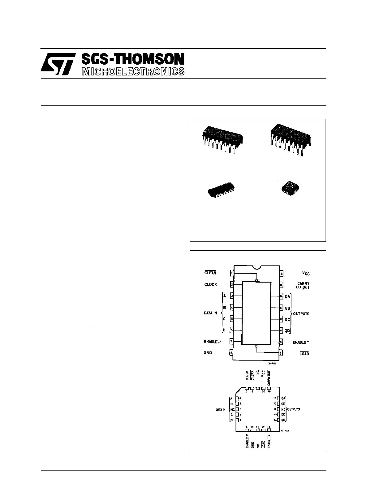
PIN CONNECTIONS (topview)
NC =
No InternalCon-
F1R
(CeramicPackage)
C1R
(Chip Carrier)
October 1993
1/16
Page 2
M54/M74HCT160/161/162/163
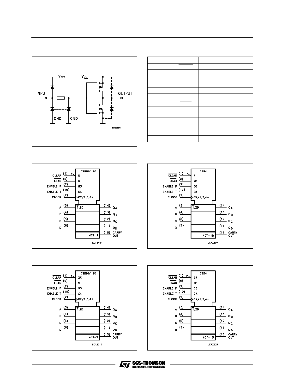
INPUT AND OUTPUT EQUIVALENT CIRCUIT
PIN DESCRIPTION
PIN No SYMBOL NAME AND FUNCTION
1 CLEAR Master Reset
2 CLOCK Clock Input (LOW to
HIGH, Edge-triggered)
3, 4, 5, 6 A, B, C, D Data Inputs
7 ENABLE P Count Enable Input
10 ENABLET Count Enable Carry Input
9 LOAD Parallel Enable Input
14, 13, 12,11QA to QD Flip Flop Outputs
15 CARRY
OUTPUT
8 GND Ground (0V)
16 V
CC
Terminal Count Output
Positive Supply Voltage
IEC LOGIC SYMBOL (HCT161)IEC LOGIC SYMBOL (HCT160)
IEC LOGIC SYMBOL (HCT162) IEC LOGIC SYMBOL (HCT163)
2/16
Page 3
TRUTH TABLE
M54/M74HCT160/161/162/163
M54/74HCT160/161 M54/74HCT162/163
INPUTS INPUTS
CLR LD PE TE CK CLR LD PE TE CK QA QB QC QD
LXXXXLXXX LLLLRESET TO ”0”
H L X X H L X X A B C D PRESET DATA
H H X L H H X L NO CHANGE NO COUNT
H H L X H H L X NO CHANGE NO COUNT
HHHH HHHH COUNT UP COUNT
H X X X X X X X NO CHANGE NO COUNT
Note: X :Don’tCare
A, B, C, D : Logi level of data inputs
Carry : CARRY =TE • QA• QB• QC• QD............ (M54/74HCT160/162)
:CARRY = TE • QA• QB• QC• QD............ (M54/74HCT161/163)
OUTPUTS
FUNCTION
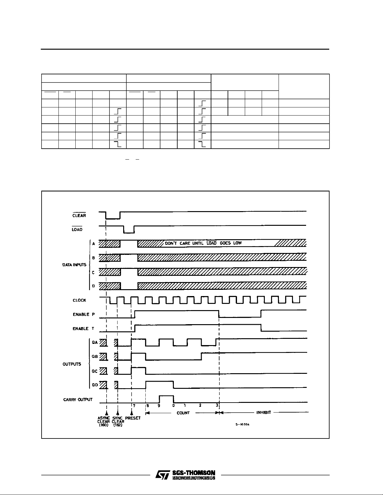
TIMING CHART (HCT160/162 : decade counter)
3/16
Page 4
M54/M74HCT160/161/162/163
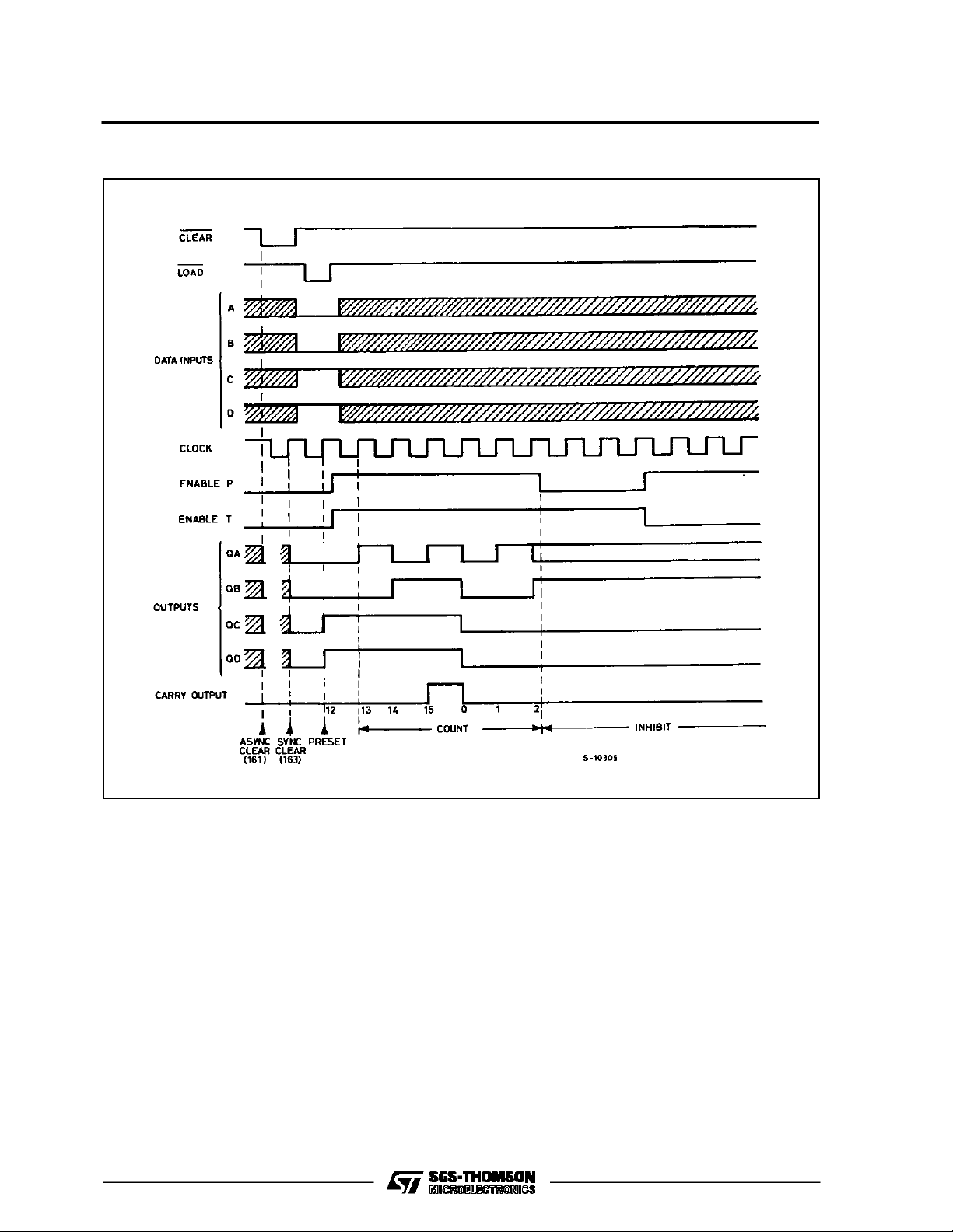
TIMING CHART (HCT161/163 : binary counter)
4/16
Page 5
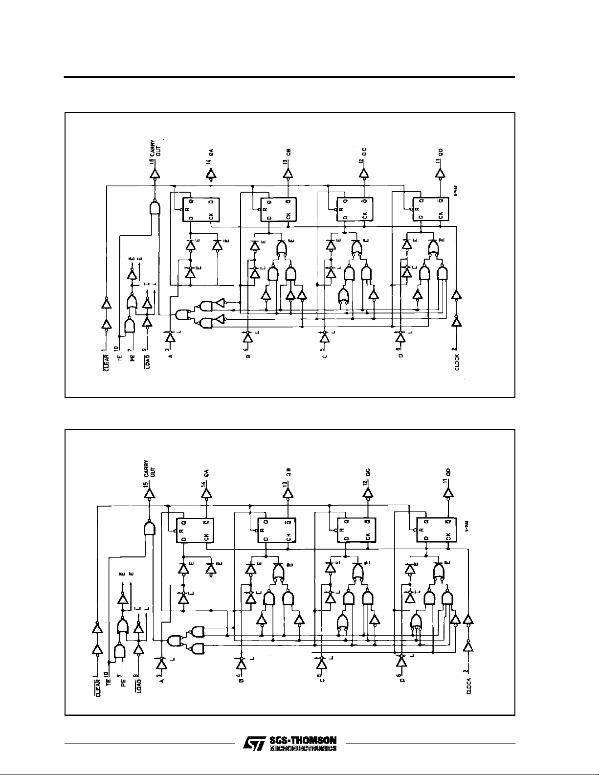
LOGIC DIAGRAM
HCT160
M54/M74HCT160/161/162/163
LOGIC DIAGRAM
HCT161
5/16
Page 6

M54/M74HCT160/161/162/163
LOGIC DIAGRAM
HCT162
LOGIC DIAGRAM
HCT163
6/16
Page 7

M54/M74HCT160/161/162/163
ABSOLU TE MAXI MU M RAT INGS
Symbol Parameter Value Unit
V
CC
V
V
O
I
IK
I
OK
I
O
I
or I
CC
P
D
T
stg
T
AbsoluteMaximumRatingsarethosevalues beyond whichdamagetothedevicemayoccur.Functionaloperation under theseconditionsis notimplied.
(*)500 mW: ≅ 65oC derateto300 mWby 10mW/oC: 65oCto85oC
RECO MM ENDED OPERATIN G C ONDI TIONS
Symbol Parameter Value Unit
V
CC
V
I
V
O
T
op
t
r,tf
Supply Voltage -0.5 to +7 V
DC Input Voltage -0.5 to VCC+ 0.5 V
I
DC Output Voltage -0.5 to VCC+ 0.5 V
DC Input Diode Current ± 20 mA
DC Output Diode Current ± 20 mA
DC Output Source Sink Current Per Output Pin ± 25 mA
DC VCCor Ground Current ± 50 mA
GND
Power Dissipation 500 (*) mW
Storage Temperature -65 to +150
Lead Temperature (10 sec) 300
L
Supply Voltage 4.5 to 5.5 V
Input Voltage 0 to V
Output Voltage 0 to V
Operating Temperature: M54HC Series
M74HC Series
CC
CC
-55 to +125
-40 to +85
Input Rise and Fall Time (VCC= 4.5 to 5.5V) 0 to 500 ns
o
C
o
C
V
V
o
C
o
C
7/16
Page 8

M54/M74HCT160/161/162/163
DC SPECIFICATIONS
Test Conditions Value
Symbol Parameter
V
High Level Input
IH
Voltage
V
Low Level Input
IL
Voltage
V
OH
High Level
Output Voltage
V
Low Level Output
OL
Voltage
Input Leakage
I
I
Current
I
Quiescent Supply
CC
Current
∆I
Additional worst
CC
case supply
current
V
CC
(V)
4.5
to
5.5
4.5
to
5.5
VI=
V
4.5
IH
or
V
IL
VI=
V
4.5
5.5
IH
or
V
IL
VI=VCCor GND ±0.1 ±1 ±1 µA
5.5 VI=VCCor GND 4 40 80 µA
5.5 Per Input pin
VI= 0.5V or
Other Inputs at
VCCor GND
T
=25oC
A
54HC and 74HC
-40 to 85oC
74HC
-55 to 125oC
54HC
Min. Typ. Max. Min. Max. Min. Max.
2.0 2.0 2.0 V
0.8 0.8 0.8 V
IO=-20 µA 4.4 4.5 4.4 4.4
I
=-4.0 mA 4.18 4.31 4.13 4.10
O
IO=20µA 0.0 0.1 0.1 0.1
I
= 4.0 mA 0.17 0.26 0.33 0.4
O
2.0 2.9 3.0 mA
V
= 2.4V
I
Unit
V
V
8/16
Page 9

M54/M74HCT160/161/162/163
AC ELECTRICAL CHARACTERISTICS (CL=50pF,Inputtr=tf=6ns)
Test Conditions Value
T
=25oC
Symbol Parameter
t
TLH
t
THL
t
PLH
t
PHL
Output Transition
Time
Propagation
Delay Time
V
CC
(V)
4.5 8151922ns
4.5 23 36 45 54 ns
A
54HC and 74HC
Min. Typ. Max. Min. Max. Min. Max.
(CK - Q)
t
t
PLH
PHL
Propagation
Delay Time
4.5 27 42 53 63 ns
(CK-CO)
t
PLH
Propagation
4.5 21 33 41 50 ns
Delay Time
(TE-CO)
t
t
f
MAX
PLH
PHL
Propagation
Delay Time
(CLEAR - Q)
Propagation
Delay Time
(CLEAR-CO)
Maximum Clock
4.5 for
26 40 50 60 ns
HCT160/161
only
4.5 for
28 43 54 65 ns
HCT160/161
only
4.5 31 49 25 21 MHz
Frequency
t
W(H)
t
W(L)
t
W(L)
Minimum Pulse
Width (CK)
Minimum Pulse
Width
(CLEAR)
Minimum Set-up
t
s
4.5 8151922ns
4.5 for
8151922ns
HCT160/161
only
4.5 11 20 25 30 ns
Time
(LOAD, PE, TE)
t
s
Minimum Set-up
4.5 5151922ns
Time
(A, B, C, D)
t
Minimum Set-up
s
Time
(CLEAR)
Minimum Hold
t
h
4.5 for
5151922ns
HCT162/163
only
4.5 5 5 8 ns
Time
t
REM
C
C
PD
Minimum
Removal Time
(CLEAR)
Input Capacitance 5 10 10 10 pF
IN
(*) Power Dissipation
4.5 for
HCT160/161
only
5151922ns
33 pF
Capacitance
(*) CPDisdefined as the valueof the IC’s internal equivalent capacitance which is calculated fromthe operating current consumption without load.
(Referto Test Circuit).Average operting current can be obtained bythe followingequation. ICC(opr) = CPD•VCC•fIN+I
-40 to 85oC
74HC
-55 to 125oC
54HC
CC
Unit
9/16
Page 10

M54/M74HCT160/161/162/163
SWITCHING CHARACTERISTICS TEST WAVEFORM
COUNT MODE CLEARMODE (HCT160/161)
PRESETMODE CLEARMODE (HCT162/163)
COUNTENABLE MODE CASCADE MODE
(fix maximum count)
10/16
Page 11

M54/M74HCT160/161/162/163
TEST CIRCUIT ICC(Opr.) TOTAL OPERATING CURRENT WHEN
USING A CAPACITIVE LOAD
When the outputs drive a capacitive load,the
total current can be calculatedas follows:
For M74HCT160/162 :
C
C
C
10
C
8
C
c
d
+
+
10
C
c
d
+
+
16
TYPICAL APPLICATION
a
∆ lCC=fCK⋅ VCC⋅
b
+
2
+
5
For M74HCT161/163 :
C
C
a
∆ lCC=fCK⋅ VCC⋅
b
+
2
+
4
Cato Ccaare the capacitors loading the outputs.
C
C
10
16
ca
ca
11/16
Page 12

M54/M74HCT160/161/162/163
Plastic DIP16 (0.25) MECHANICAL DATA
DIM.
MIN. TYP. MAX. MIN. TYP. MAX.
a1 0.51 0.020
B 0.77 1.65 0.030 0.065
b 0.5 0.020
b1 0.25 0.010
D 20 0.787
E 8.5 0.335
e 2.54 0.100
e3 17.78 0.700
F 7.1 0.280
I 5.1 0.201
L 3.3 0.130
Z 1.27 0.050
mm inch
12/16
P001C
Page 13

M54/M74HCT160/161/162/163
Ceramic DIP16/1 MECHANICAL DATA
DIM.
MIN. TYP. MAX. MIN. TYP. MAX.
A 20 0.787
B 7 0.276
D 3.3 0.130
E 0.38 0.015
e3 17.78 0.700
F 2.29 2.79 0.090 0.110
G 0.4 0.55 0.016 0.022
H 1.17 1.52 0.046 0.060
L 0.22 0.31 0.009 0.012
M 0.51 1.27 0.020 0.050
N 10.3 0.406
P 7.8 8.05 0.307 0.317
Q 5.08 0.200
mm inch
P053D
13/16
Page 14

M54/M74HCT160/161/162/163
SO16 (Narrow) MECHANICAL DATA
DIM.
MIN. TYP. MAX. MIN. TYP. MAX.
A 1.75 0.068
a1 0.1 0.2 0.004 0.007
a2 1.65 0.064
b 0.35 0.46 0.013 0.018
b1 0.19 0.25 0.007 0.010
C 0.5 0.019
c1 45° (typ.)
D 9.8 10 0.385 0.393
E 5.8 6.2 0.228 0.244
e 1.27 0.050
e3 8.89 0.350
F 3.8 4.0 0.149 0.157
G 4.6 5.3 0.181 0.208
L 0.5 1.27 0.019 0.050
M 0.62 0.024
S8°(max.)
mm inch
14/16
P013H
Page 15

M54/M74HCT160/161/162/163
PLCC20 MECHANICAL DATA
DIM.
MIN. TYP. MAX. MIN. TYP. MAX.
A 9.78 10.03 0.385 0.395
B 8.89 9.04 0.350 0.356
D 4.2 4.57 0.165 0.180
d1 2.54 0.100
d2 0.56 0.022
E 7.37 8.38 0.290 0.330
e 1.27 0.050
e3 5.08 0.200
F 0.38 0.015
G 0.101 0.004
M 1.27 0.050
M1 1.14 0.045
mm inch
P027A
15/16
Page 16

M54/M74HCT160/161/162/163
Information furnished is believed to be accurate and reliable. However, SGS-THOMSON Microelectronics assumes no responsability for the
consequences of use of such information nor for any infringement of patents or other rights of third parties which may results from its use. No
license is granted byimplication or otherwise under any patent or patentrights of SGS-THOMSON Microelectronics. Specificationsmentioned
in this publication are subject to change without notice. This publication supersedes and replaces all information previously supplied.
SGS-THOMSON Microelectronicsproducts are not authorized foruse ascritical componentsin life support devices or systems without express
written approval of SGS-THOMSON Microelectonics.
1994 SGS-THOMSON Microelectronics - All Rights Reserved
Australia - Brazil - France - Germany - Hong Kong - Italy - Japan - Korea - Malaysia - Malta - Morocco - The Netherlands -
Singapore -Spain - Sweden- Switzerland -Taiwan - Thailand - UnitedKingdom - U.S.A
SGS-THOMSON Microelectronics GROUP OF COMPANIES
16/16
 Loading...