

Page 1
HCT157QUAD 2 CHANNEL MULTIPLEXER
HCT158 QUAD2 CHANNEL MULTIPLEXER (INV.)
.HIGH SPEED
tPD= 21 ns (TYP.) AT VCC=5V
.LOWPOWER DISSIPATION
ICC=4 µA (MAX.) AT TA=25 °C
.COMPATIBLE WITHTTL OUTPUTS
VIH= 2V (MIN.) VIL= 0.8V (MAX)
.OUTPUT DRIVE CAPABILITY
10 LSTTL LOADS
.SYMMETRICAL OUTPUT IMPEDANCE
IOH =IOL= 4 mA (MIN.)
.BALANCEDPROPAGATION DELAYS
t
PLH=tPHL
.PIN AND FUNCTION COMPATIBLE
WITH 54/74LS157/158
M54HCT157/158
M74HCT157/158
B1R
(PlasticPackage)
M1R
(MicroPackage)
ORDER CODES :
M54HC TXXX F 1R M74H CTXXXM1R
M74HC TXXX B1R M74HCT XXX C1R
F1R
(CeramicPackage)
C1R
(Chip Carrier)
DESCRIPTION
The M54/74HCT157 and the M54/74HCT158 are
high speed CMOS QUAD 2-CHANNEL MULTIPLEXERs fabricated withsilicongate C2MOStechnology. They achieve the high speed operation
similar to equivalent LSTTL while maintaining the
CMOS low power dissipation.
These devices consist of four 2-input digital multiplexerswith common select and strobe inputs.The
HCT158 is an inverting multiplexer while the
HCT157 is a non-inverting multiplexer. When the
STROBEinput is held High, selection of data is inhibited and all the outputs become Low in the
M74HCT157 and High in theM74HCT158. TheSELECT decoding determines whether the A or B inputs get routed to theircorresponding Y outputs.All
inputs are equipped with protection circuits against
static discharge and transient excess voltage.
M54/74HCT devices are designed to directlyinterfaceHSC2MOSsystemswith TTLandNMOScomponents. They are also plug in replacements for
LSTTL devices giving a reduction of power consumption.
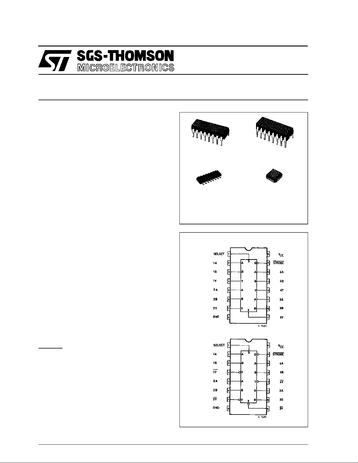
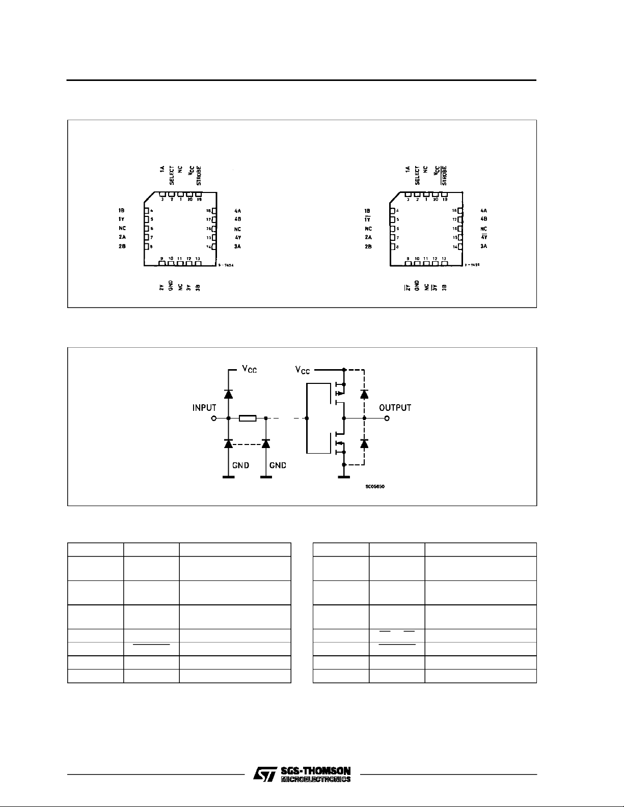
PIN CONNECTIONS(top view)
HCT157
HCT158
NC =
No Internal
Connection
April1993
1/11
Page 2
M54/M74HCT157 M54/M74HCT158
CHIP CARRIER
HCT157 HCT158
INPUT AND OUTPUT EQUIVALENT CIRCUIT
PIN DESCRIPTION (for HCT157)
PIN No SYMBOL NAME AND FUNCTION
1 SELECT Common Data Select
Input
2, 5, 11, 14 1A to 4A Data Inputs From
Source A
3, 6, 10, 13 1B to 4B Data Inputs From
Source B
4, 7, 9, 12 1Y to 4Y Multiplexer Output
15 STROBE StrobeInput
8 GND Ground (0V)
16 V
2/11
CC
Positive Supply Voltage
PIN DESCRIPTIO N (for HCT158)
PIN No SYMBOL NAME AND FUNCTION
1 SELECT Common Data Select
Input
2, 5, 11, 14 1A to 4A Data Inputs From
Source A
3, 6, 10, 13 1B to 4B Data Inputs From
Source B
4, 7, 9, 12 1Y to 4Y Multiplexer Output
15 STROBE Strobe Input
8 GND Ground (0V)
16 V
CC
Positive Supply Voltage
Page 3
M54/M74HCT157 M54/M74HCT158
TRUTH TABLE
INPUTS OUTPUTS
STROBE SELECT A B Y (HCT157) Y (HCT158)
HXXXLH
LLLXLH
LLHXHL
LHXLLH
LHXHHL
X:DON’TCARE
IEC LOGIC SYMBOL
HCT157 HCT158
LOGIC DIAGRAM
HCT157 HCT158
3/11
Page 4
M54/M74HCT157 M54/M74HCT158
ABSOLU TE MAXIMUM RATINGS
Symbol Parameter Value Unit
V
CC
V
V
O
I
IK
I
OK
I
O
I
or I
CC
P
D
T
stg
T
L
AbsoluteMaximumRatingsarethosevaluesbeyondwhichdamagetothedevicemayoccur.Functionaloperationunder theseconditionisnotimplied.
(*)500 mW:≅65oC derate to300 mW by 10mW/oC: 65oCto85oC
RECO MM ENDED OPERAT I N G CONDI TI ONS
Symbol Parameter Value Unit
V
CC
V
I
V
O
T
op
t
r,tf
Supply Voltage -0.5 to +7 V
DC Input Voltage -0.5 to VCC+ 0.5 V
I
DC Output Voltage -0.5 to VCC+ 0.5 V
DC Input Diode Current ± 20 mA
DC Output Diode Current ± 20 mA
DC Output Source Sink Current Per Output Pin ± 25 mA
DC VCCor Ground Current ± 50 mA
GND
Power Dissipation 500 (*) mW
Storage Temperature -65 to +150
Lead Temperature (10 sec) 300
Supply Voltage 4.5 to 5.5 V
Input Voltage 0 to V
Output Voltage 0 to V
Operating Temperature: M54HC Series
M74HC Series
CC
CC
-55 to +125
-40 to +85
Input Rise and Fall Time (VCC= 4.5 to 5.5V) 0 to 500 ns
o
C
o
C
V
V
o
C
o
C
4/11
Page 5

DC SPECIFICATIO NS
Symbol Parameter
V
V
V
V
I
∆I
High Level Input
IH
Voltage
Low Level Input
IL
Voltage
High Level
OH
Output Voltage
Low Level Output
OL
Voltage
Input Leakage
I
I
Current
Quiescent Supply
CC
Current
Additional worst
CC
case supply
current
M54/M74HCT157 M54/M74HCT158
Test Conditions Value
T
=25oC
V
(V)
4.5
CC
A
54HC and 74HC
Min. Typ. Max. Min. Max. Min. Max.
2.0 2.0 2.0 V
to
5.5
4.5
to
5.5
VI=
IO=-20 µA 4.4 4.5 4.4 4.4
V
IH
4.5
or
I
=-4.0 mA 4.18 4.31 4.13 4.10
O
V
IL
VI=
IO=20µA 0.0 0.1 0.1 0.1
V
IH
4.5
or
I
= 4.0 mA 0.17 0.26 0.33 0.4
O
V
IL
VI=VCCor GND ±0.1 ±1 ±1 µA
5.5
5.5 VI=VCCor GND 4 40 80 µA
5.5 Per Input pin
VI= 0.5V or
V
= 2.4V
I
Other Inputs at
VCCor GND
IO=0
-40 to 85oC
74HC
-55 to 125oC
54HC
Unit
0.8 0.8 0.8 V
2.0 2.9 3.0 mA
V
V
5/11
Page 6

M54/M74HCT157 M54/M74HCT158
AC ELECTRICAL CHARACTERISTICS (CL=50pF,Inputtr=tf=6ns)
Test Conditions Value
T
=25oC
Symbol Parameter
t
TLH
t
THL
t
PLH
t
PHL
Output Transition
Time
Propagation
Delay Time
V
CC
(V)
4.5 8151922ns
4.5 16 25 31 38 ns
A
54HC and 74HC
Min. Typ. Max. Min. Max. Min. Max.
(A, B - Y)
t
t
PLH
PHL
Propagation
Delay Time
4.5 19 30 38 45 ns
(SELECT - Y)
t
t
PLH
PHL
Propagation
Delay Time
4.5 17 27 34 41 ns
(STROBE - Y)
C
C
PD
(*) CPDisdefinedas the value ofthe IC’s internal equivalent capacitance which is calculatedfromthe operatingcurrent consumption withoutload.
(RefertoTestCircuit).Average opertingcurrent can be obtained bythe followingequation. ICC(opr) = CPD•VCC•fIN+ICC/4(per channel)
Input Capacitance 5 10 10 10 pF
IN
(*) Power Dissipation
Capacitance
HCT157 50 pF
HCT158 60 pF
-40 to 85oC
74HC
-55 to 125oC
54HC
Unit
SWITCHING CHARACTERISTICS TEST CIRCUIT
TEST CIRCUIT ICC(Opr.)
INPUTWAVEFORM ISTHE SAME AS THATIN CASEOF
SWITCHINGCHARACTERISTICSTEST.
6/11
Page 7

M54/M74HCT157 M54/M74HCT158
Plastic DIP16 (0.25) MECHANICAL DATA
DIM.
MIN. TYP. MAX. MIN. TYP. MAX.
a1 0.51 0.020
B 0.77 1.65 0.030 0.065
b 0.5 0.020
b1 0.25 0.010
D 20 0.787
E 8.5 0.335
e 2.54 0.100
e3 17.78 0.700
F 7.1 0.280
I 5.1 0.201
L 3.3 0.130
Z 1.27 0.050
mm inch
P001C
7/11
Page 8

M54/M74HCT157 M54/M74HCT158
Ceramic DIP16/1 MECHANICAL DATA
DIM.
MIN. TYP. MAX. MIN. TYP. MAX.
A 20 0.787
B 7 0.276
D 3.3 0.130
E 0.38 0.015
e3 17.78 0.700
F 2.29 2.79 0.090 0.110
G 0.4 0.55 0.016 0.022
H 1.17 1.52 0.046 0.060
L 0.22 0.31 0.009 0.012
M 0.51 1.27 0.020 0.050
N 10.3 0.406
P 7.8 8.05 0.307 0.317
Q 5.08 0.200
mm inch
8/11
P053D
Page 9

M54/M74HCT157 M54/M74HCT158
SO16 (Narrow) MECHANICAL DATA
DIM.
MIN. TYP. MAX. MIN. TYP. MAX.
A 1.75 0.068
a1 0.1 0.2 0.004 0.007
a2 1.65 0.064
b 0.35 0.46 0.013 0.018
b1 0.19 0.25 0.007 0.010
C 0.5 0.019
c1 45° (typ.)
D 9.8 10 0.385 0.393
E 5.8 6.2 0.228 0.244
e 1.27 0.050
e3 8.89 0.350
F 3.8 4.0 0.149 0.157
G 4.6 5.3 0.181 0.208
L 0.5 1.27 0.019 0.050
M 0.62 0.024
S8°(max.)
mm inch
P013H
9/11
Page 10

M54/M74HCT157 M54/M74HCT158
PLCC20 MECHANICAL DATA
DIM.
MIN. TYP. MAX. MIN. TYP. MAX.
A 9.78 10.03 0.385 0.395
B 8.89 9.04 0.350 0.356
D 4.2 4.57 0.165 0.180
d1 2.54 0.100
d2 0.56 0.022
E 7.37 8.38 0.290 0.330
e 1.27 0.050
e3 5.08 0.200
F 0.38 0.015
G 0.101 0.004
M 1.27 0.050
M1 1.14 0.045
mm inch
10/11
P027A
Page 11

M54/M74HCT157 M54/M74HCT158
Information furnished is believed to be accurate and reliable. However, SGS-THOMSON Microelectronics assumes no responsability for the
consequences of use of such information nor for any infringement of patents orother rights of third parties which may results from its use. No
license is grantedby implication or otherwise underany patentor patent rights of SGS-THOMSON Microelectronics. Specificationsmentioned
in this publicationare subject to changewithout notice. This publication supersedes andreplaces all information previously supplied.
SGS-THOMSON Microelectronicsproductsare notauthorized foruse ascritical componentsin life supportdevices or systemswithout express
written approval of SGS-THOMSON Microelectonics.
1994 SGS-THOMSON Microelectronics- All RightsReserved
Australia - Brazil - France - Germany - HongKong - Italy - Japan - Korea - Malaysia - Malta - Morocco - The Netherlands -
Singapore - Spain - Sweden - Switzerland -Taiwan - Thailand - United Kingdom - U.S.A
SGS-THOMSON Microelectronics GROUPOF COMPANIES
11/11
 Loading...