

Page 1
3 TO8 LINE DECODER/LATCH (INVERTING)
.HIGH SPEED
tPD= 17 ns(TYP.) AT VCC=5V
.LOWPOWER DISSIPATION
ICC=4µA(MAX.) AT TA=25 °C
.COMPATIBLE WITH TTL OUTPUTS
VIH= 2V (MIN.) VIL= 0.8V (MAX)
.OUTPUT DRIVE CAPABILITY
10 LSTTLLOADS
.SYMMETRICALOUTPUT IMPEDANCE
IOH =IOL= 4 mA(MIN.)
.BALANCEDPROPAGATION DELAYS
t
PLH=tPHL
.PIN ANDFUNCTION COMPATIBLE
WITH 54/74LS137
DESCRIPTION
TheM54/74HCT137isa highspeed CMOS3TO8LINE
DECODE R/ L A TC H (I NVER TI NG) fabri cated in silic o n
gateC2MOStechnol ogy.IthasthesamehighspeedperformanceofLSTTLcombinedwithtrueCMOSlowpower
consumption.Thisdeviceisa 3 to 8 linedecod erwithlatches on the three address inputs. When GL goes from low
tohigh, the addres s presentat theselect input s(A,B and
C) isstored in the latches. Aslong as GLremains high no
addre ss cha nges wi llbe r ecog nized . Outputenable pins
G1an d G2,contro l thestateof theoutputsindependently
oftheselectorlatch-enab le inputs.All theoutputsarehigh
unless G1 is h igh and G2 is low. The HC137 is ideally
suited for the implement ation of glitch -fre e de code rs in
stored-add re ss appl icatio ns in bus orien ted systems.All
inputs are equipped with protectio n ci rcuit s against static
discharge and transien t excess voltage.Thi s integrate d
circuit has input and output characteristics that are fully
compatible with 54/74 LSTTL logic families. M54/74HCT
devicesaredesignedtodirectlyinterfa ceHSC2MOSsystemswithTTLandNMOScomponents.Theyarealso
plugin replacements for LSTTL devices giving a reductionof power consumption.
M54HCT137
M74HCT137
B1R
(PlasticPackage)
M1R
(MicroPackage)
ORDER CODES :
M54HC T137F1R M74H CT137M1R
M74HC T137B1R M74HCT137C1R
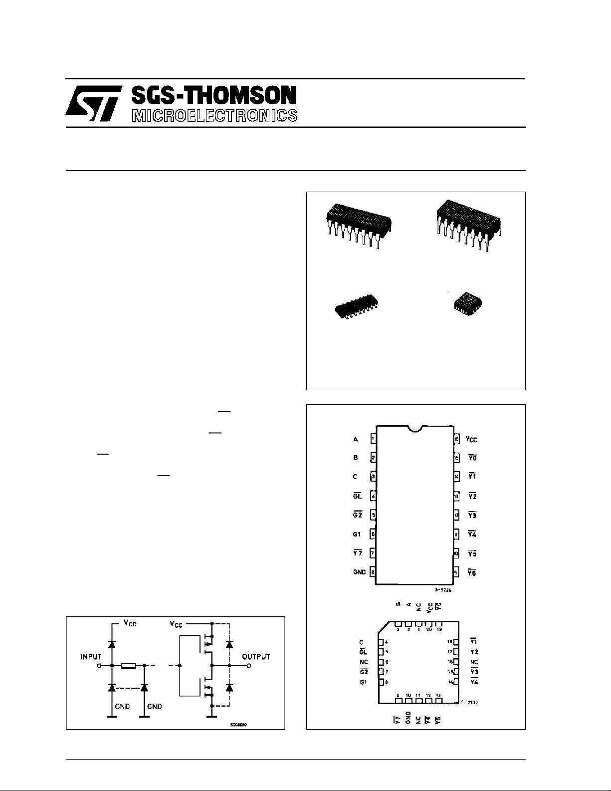
PIN CONNECTIONS(top view)
F1R
(CeramicPackage)
C1R
(Chip Carrier)
INPUT AND OUTPUT EQUIVALENT CIRCUIT
February 1993
NC =
No Internal
Connection
1/12
Page 2
M54/M74HCT137
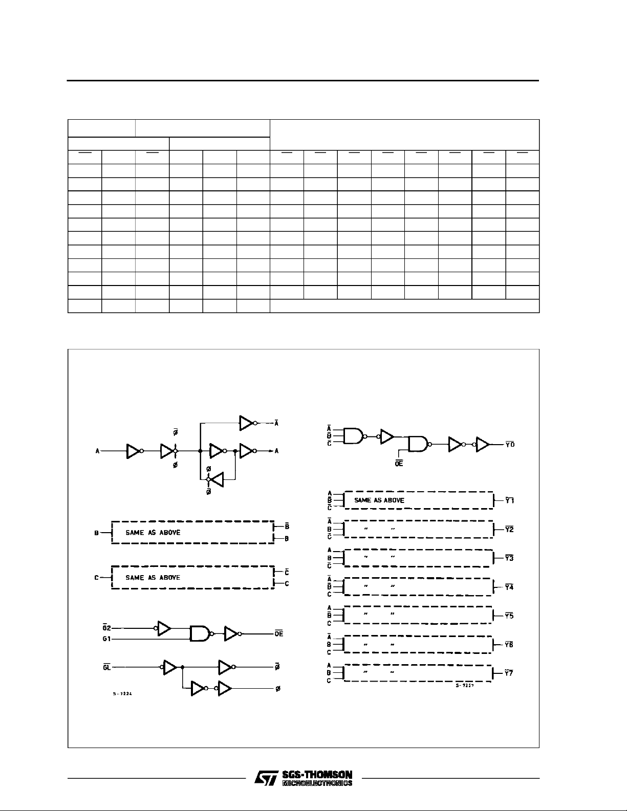
TRUTH TABLE
INPUTS
ENABLE SELECT
GL G1 G2 C B A Y0 Y1 Y2 Y3 Y4 Y5 Y6 Y7
XLXXXXHHHHHHHH
XXHXXXHHHHHHHH
LHL L L LLHHHHHHH
LHL L LHHLHHHHHH
LHL LHLHHLHHHHH
LHL LHHHHHLHHHH
LHLHL LHHHHLHHH
LHLHLHHHHHHLHH
LHLHHLHHHHHHLH
LHLHHHHHHHHHHL
H H L X X X Outputs corresponding to stored address L: all others H
OUTPUTS
LOGI C DIAG RAM
2/12
Page 3
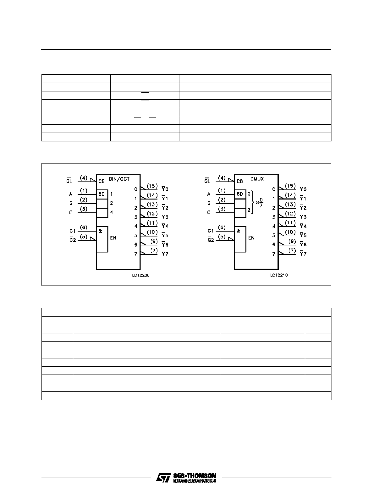
PIN DESCRIPTION
PIN No SYMBOL NAME AND FUNCTION
1, 2, 3 A to C Data Inputs
4 GL Latch Enable Input (Active LOW)
5 G2 Data Enable Input (Active LOW)
6 G1 Data Enable Input (Active HIGH)
15, 14, 13, 12, 11, 10, 9, 7 Y0 to Y7 Multiplexer Outputs
8 GND Ground (0V)
16 V
CC
Positive Supply Voltage
IEC LOGIC SYMBOLS
M54/M74HCT137
ABSOLU TE M AXI MU M R AT INGS
Symbol Parameter Value Unit
V
CC
V
V
O
I
IK
I
OK
I
O
I
or I
CC
P
D
T
stg
T
AbsoluteMaximumRatingsarethosevaluesbeyondwhichdamagetothedevice mayoccur. Functionaloperationunder theseconditionisnotimplied.
(*)500 mW:≅ 65oC derateto 300 mWby 10mW/oC: 65oCto85oC
Supply Voltage -0.5 to +7 V
DC Input Voltage -0.5 to VCC+ 0.5 V
I
DC Output Voltage -0.5 to VCC+ 0.5 V
DC Input Diode Current ± 20 mA
DC OutputDiode Current ± 20 mA
DC Output Source Sink Current Per Output Pin ± 25 mA
DC VCCor Ground Current ± 50 mA
GND
Power Dissipation 500 (*) mW
Storage Temperature -65 to +150
Lead Temperature (10 sec) 300
L
o
C
o
C
3/12
Page 4
M54/M74HCT137
RECO MM ENDED OPERATI N G CO NDITI O NS
Symbol Parameter Value Unit
V
V
V
T
t
r,tf
DC SPECIFICATIO NS
Symbol Parameter
V
V
V
OH
V
OL
I
I
CC
∆I
Supply Voltage 4.5 to 5.5 V
CC
Input Voltage 0 to V
I
Output Voltage 0 to V
O
Operating Temperature: M54HC Series
op
M74HC Series
CC
CC
-55 to +125
-40 to +85
Input Rise and Fall Time (VCC= 4.5 to 5.5V) 0 to 500 ns
Test Conditions Value
T
High Level Input
IH
Voltage
V
(V)
4.5
=25oC
CC
A
54HC and 74HC
Min. Typ. Max. Min. Max. Min. Max.
2.0 2.0 2.0 V
to
-40 to 85oC
74HC
-55 to 125oC
5.5
Low Level Input
IL
Voltage
4.5
to
0.8 0.8 0.8 V
5.5
High Level
Output Voltage
Low Level Output
Voltage
Input Leakage
I
Current
Quiescent Supply
VI=
IO=-20 µA 4.4 4.5 4.4 4.4
V
IH
4.5
or
I
=-4.0 mA 4.18 4.31 4.13 4.10
O
V
IL
VI=
IO=20µA 0.0 0.1 0.1 0.1
V
IH
4.5
or
I
= 4.0 mA 0.17 0.26 0.33 0.4
O
V
IL
VI=VCCor GND ±0.1 ±1 ±1 µA
5.5
5.5 VI=VCCor GND 4 40 80 µA
Current
Additional worst
CC
case supply
current
5.5 Per Input pin
V
= 0.5V or
I
VI= 2.4V
2.0 2.9 3.0 mA
Other Inputs at
VCCor GND
IO=0
54HC
V
V
o
C
o
C
Unit
V
V
4/12
Page 5

M54/M74HCT137
AC ELECTRICAL CHARACTERISTICS (CL=50pF,Inputtr=tf=6ns)
Test Conditions Value
T
=25oC
Symbol Parameter
t
t
t
t
TLH
THL
PLH
PHL
Output Transition
Time
Propagation
Delay Time
V
CC
(V)
4.5 8151922
4.5 17 27 34 41
A
54HC and 74HC
Min. Typ. Max. Min. Max. Min. Max.
(G1 - Y)
t
t
PLH
PHL
Propagation
Delay Time
4.5 18 28 35 42
(G2 - Y)
t
t
PLH
PHL
Propagation
Delay Time
4.5 25 39 49 59
(GL - Y)
t
t
PLH
PHL
Propagation
Delay Time
4.5 24 37 46 56
(A, B, C - Y)
t
W(L)
Minimum Pulse
4.5 8151922
Width
(GL)
t
Minimum Set-up
s
4.5 5 6 8
Time
(A, B, C - GL)
t
h
Minimum Hold
4.5 5 6 8
Time
(A, B, C - GL)
C
C
PD
Input Capacitance 5 10 10 10 pF
IN
(*) Power Dissipation
58
Capacitance
(*) CPDisdefined as the valueof the IC’s internal equivalent capacitance whichis calculated from the operating current consumption without load.
(Referto Test Circuit).Average opertingcurrentcan be obtained by the followingequation. ICC(opr) = CPD•VCC•fIN+I
-40 to 85oC
74HC
-55 to 125oC
54HC
CC
Unit
ns
ns
ns
ns
ns
ns
ns
ns
pF
5/12
Page 6

M54/M74HCT137
TEST CIRCUIT ICC(Opr.)
INPUTWAVEFORM IS THE SAME AS THAT IN CASE OF SWITCHINGCHARACTERISTICSTEST.
TYPICAL APPLICATION
6/12
Page 7

SWITCHING CHARACTERISTICS TEST WAVEFORM
M54/M74HCT137
7/12
Page 8

M54/M74HCT137
Plastic DIP16 (0.25) MECHANICAL DATA
DIM.
MIN. TYP. MAX. MIN. TYP. MAX.
a1 0.51 0.020
B 0.77 1.65 0.030 0.065
b 0.5 0.020
b1 0.25 0.010
D 20 0.787
E 8.5 0.335
e 2.54 0.100
e3 17.78 0.700
F 7.1 0.280
I 5.1 0.201
L 3.3 0.130
Z 1.27 0.050
mm inch
8/12
P001C
Page 9

Ceramic DIP16/1 MECHANICAL DATA
M54/M74HCT137
DIM.
MIN. TYP. MAX. MIN. TYP. MAX.
A 20 0.787
B 7 0.276
D 3.3 0.130
E 0.38 0.015
e3 17.78 0.700
F 2.29 2.79 0.090 0.110
G 0.4 0.55 0.016 0.022
H 1.17 1.52 0.046 0.060
L 0.22 0.31 0.009 0.012
M 0.51 1.27 0.020 0.050
N 10.3 0.406
P 7.8 8.05 0.307 0.317
Q 5.08 0.200
mm inch
P053D
9/12
Page 10

M54/M74HCT137
SO16 (Narrow) MECHANICAL DATA
DIM.
MIN. TYP. MAX. MIN. TYP. MAX.
A 1.75 0.068
a1 0.1 0.2 0.004 0.007
a2 1.65 0.064
b 0.35 0.46 0.013 0.018
b1 0.19 0.25 0.007 0.010
C 0.5 0.019
c1 45° (typ.)
D 9.8 10 0.385 0.393
E 5.8 6.2 0.228 0.244
e 1.27 0.050
e3 8.89 0.350
F 3.8 4.0 0.149 0.157
G 4.6 5.3 0.181 0.208
L 0.5 1.27 0.019 0.050
M 0.62 0.024
S8°(max.)
mm inch
10/12
P013H
Page 11

PLCC20 MECHANICAL DATA
M54/M74HCT137
DIM.
MIN. TYP. MAX. MIN. TYP. MAX.
A 9.78 10.03 0.385 0.395
B 8.89 9.04 0.350 0.356
D 4.2 4.57 0.165 0.180
d1 2.54 0.100
d2 0.56 0.022
E 7.37 8.38 0.290 0.330
e 1.27 0.050
e3 5.08 0.200
F 0.38 0.015
G 0.101 0.004
M 1.27 0.050
M1 1.14 0.045
mm inch
P027A
11/12
Page 12

M54/M74HCT137
Information furnished is believed to be accurate and reliable. However, SGS-THOMSON Microelectronics assumes no responsability for the
consequences of use of such information nor for any infringement of patents or other rights of third partieswhich may results from its use. No
license is granted byimplication or otherwise under any patent or patentrights of SGS-THOMSON Microelectronics. Specificationsmentioned
in this publication are subject to change without notice. This publication supersedes and replaces all information previously supplied.
SGS-THOMSON Microelectronicsproducts are not authorized foruse ascritical componentsin life support devices or systems without express
written approval of SGS-THOMSON Microelectonics.
1994 SGS-THOMSON Microelectronics - All Rights Reserved
Australia - Brazil - France - Germany - Hong Kong - Italy - Japan - Korea- Malaysia - Malta - Morocco - The Netherlands -
Singapore -Spain - Sweden- Switzerland - Taiwan - Thailand - UnitedKingdom - U.S.A
SGS-THOMSON Microelectronics GROUP OF COMPANIES
12/12
 Loading...