

Page 1
.HIGH SPEED
tPD= 12 ns(TYP.) AT VCC=5V
.LOWPOWER DISSIPATION
ICC=4µA(MAX.) AT 25 °C
.OUTPUT DRIVE CAPABILITY
15 LSTTLLOADS
.BALANCEDPROPAGATION DELAYS
t
PLH=tPHL
.SYMMETRICALOUTPUT IMPEDANCE
IOL=IOH = 6 mA (MIN.)
.COMPATIBLE WITHTTL OUTPUTS
VIH= 2V(MIN.) VIL= 0.8V(MAX)
.PIN AND FUNCTION COMPATIBLE
WITH 54/74LS125/126
DESCRIPTION
The M54/74HCT125/126 are high speed CMOS
QUAD BUS BUFFER (3-STATE) FABRICATED IN
SILICONGATEC2MOStechnology. They havethe
same high speed performance ofLSTTLcombined
withtrue CMOS lowpowerconsumption. Thesedevicesrequire the same 3-STATE control input G to
be takenhigh to makethe output gointothehigh impedancestate.This integrated circuit has input and
outputcharacteristics that are fully compatible with
54/74 LSTTL logic families. M54/74HCT devices
are designed to directly interface HSC2MOS systems with TTL and NMOS components. They are
also plugin replacements forLSTTL devices giving
a reduction of power consumption. All inputs are
equipped with protection circuits against static discharge and transientexcessvoltage.
M54/74HCT125
M54/74HCT126
QUAD BUS BUFFERS (3-STATE)
B1R
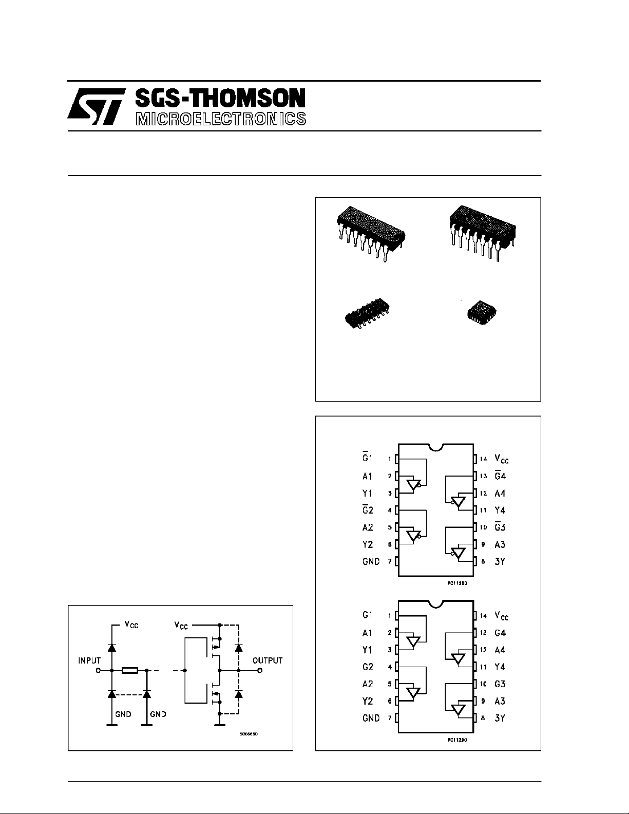
(PlasticPackage)
M1R
(MicroPackage)
ORDER CODES :
M54HC TXXXF1 R M74H CTXXXM1 R
M74HC TXXXB1R M74HCT XXXC1R
PIN CONNECTIONS (topview)
HCT125
F1R
(CeramicPackage)
C1R
(Chip Carrier)
INPUT AND OUTPUT EQUIVALENT CIRCUIT
October 1993
HCT126
NC =
No Internal
Connection
1/10
Page 2
M54/M74HCT125/126
CHIP CARRIER
HCT125 HCT126
TRUTH TABLE (HCT125 )
AGY
XHZ
LLL
HLH
PIN DESCRIPTION (HCT125)
PIN No SYMBOL NAME AND FUNCTION
1, 4, 10, 13 G1 to G4 Output Enable Input
2, 5, 9, 12 A1 to A4 Data Inputs
3, 6, 8, 11 Y1 to Y4 Data Outputs
7 GND Ground (0V)
14 V
CC
Positive Supply Voltage
IEC LOGIC SYMBOLS
HCT125 HCT126
TRUTH TABLE (HCT12 6)
AGY
XLZ
LHL
HHH
PIN DESCRIPTION (HC T126)
PIN No SYMBOL NAME AND FUNCTION
1, 4, 10, 13 G1 to G4 Output Enable Input
2, 5, 9, 12 A1 to A4 Data Inputs
3, 6, 8, 11 Y1 to Y4 Data Outputs
7 GND Ground (0V)
14 V
CC
Positive Supply Voltage
2/10
Page 3
CIR CUI T DI A GR AM
HCT125 HCT126
ABSOLU TE M AXIMU M R AT INGS
M54/M74HCT125/126
Symbol Parameter Value Unit
V
CC
V
V
O
I
IK
I
OK
I
O
I
or I
CC
P
D
T
stg
T
L
AbsoluteMaximum Ratingsarethosevalues beyond whichdamage tothedevicemayoccur.Functionaloperation under theseconditionsis notimplied.
(*)500 mW: ≅ 65oC derate to300mW by 10mW/oC: 65oCto85oC
Supply Voltage -0.5 to +7 V
DC Input Voltage -0.5 to VCC+ 0.5 V
I
DC Output Voltage -0.5 to VCC+ 0.5 V
DC Input Diode Current ± 20 mA
DC Output Diode Current ± 20 mA
DC Output Source Sink Current Per Output Pin ± 35 mA
DC VCCor Ground Current ± 70 mA
GND
Power Dissipation 500 (*) mW
Storage Temperature -65 to +150
Lead Temperature (10 sec) 300
o
C
o
C
RECO MM ENDED OPERAT I N G C ONDITI ONS
Symbol Parameter Value Unit
V
T
t
V
V
r,tf
Supply Voltage 4.5 to 5.5 V
CC
Input Voltage 0 to V
I
Output Voltage 0 to V
O
Operating Temperature: M54HC Series
op
M74HC Series
CC
CC
-55 to +125
-40 to +85
Input Rise and Fall Time (VCC= 4.5 to 5.5V) 0 to 500 ns
V
V
o
C
o
C
3/10
Page 4

M54/M74HCT125/126
DC SPECIFICATIONS
Symbol Parameter
V
V
V
V
I
I
∆I
High Level Input
IH
Voltage
Low Level Input
IL
Voltage
High Level
OH
Output Voltage
Low Level Output
OL
Voltage
Input Leakage
I
I
Current
Quiescent Supply
CC
Current
3 State Output
OZ
Off State Current
Additional worst
CC
case supply
current
Test Conditions Value
V
(V)
4.5
CC
=25oC
A
54HC and 74HC
Min. Typ. Max. Min. Max. Min. Max.
2.0 2.0 2.0 V
-40 to 85oC
74HC
-55 to 125oC
54HC
Unit
T
to
5.5
4.5
0.8 0.8 0.8 V
to
5.5
VI=
IO=-20 µA 4.4 4.5 4.4 4.4
V
IH
4.5
or
I
=-6.0 mA 4.18 4.31 4.13 4.10
O
V
IL
VI=
IO=20µA 0.0 0.1 0.1 0.1
V
IH
4.5
or
I
= 6.0 mA 0.17 0.26 0.33 0.4
O
V
IL
VI=VCCor GND ±0.1 ±1 ±1 µA
5.5
5.5 VI=VCCor GND 4 40 80 µA
VI=VIHor V
6.0
VO=VCCor GND
5.5 Per Input pin
IL
±0.5 ±5 ±10 µA
2.0 2.9 3.0 mA
VI= 0.5V or
VI= 2.4V
Other Inputs at
V
or GND
CC
IO=0
V
V
AC ELECTRICAL CHARACTERISTICS (Input tr=tf=6ns)
Test Conditions Value
=25oC
T
Symbol Parameter
t
TLH
t
THL
t
PLH
t
PHL
t
PZL
t
PZH
t
PLZ
t
PHZ
C
C
PD
Output Transition
Time
Propagation
Delay Time
3 State Output
Enable Time
3 State Output
Disable Time
Input Capacitance 5 10 10 10 pF
IN
(*) Power Dissipation
C
V
CC
(V)
L
(pF)
4.5 50 7 12 15 18 ns
4.5 50 13 21 26 32 ns
4.5 150 17 27 34 41 ns
4.5 50 RL=1KΩ 15 24 30 36 ns
4.5 150 R
=1KΩ 19 30 38 45 ns
L
4.5 50 RL=1KΩ 17 24 30 36 ns
A
54HC and 74HC
Min. Typ. Max. Min. Max. Min. Max.
56
Capacitance
(*) CPDisdefined asthe valueofthe IC’s internal equivalent capacitance which is calculated from the operatingcurrent consumption withoutload.
(RefertoTest Circuit).Average operting current can be obtained by the followingequation. ICC(opr) = CPD•VCC•fIN+I
4/10
-40 to 85oC
74HC
-55 to 125oC
54HC
CC
Unit
pF
Page 5

TEST CIRCUIT ICC(Opr.)
HCT125
HCT126
M54/M74HCT125/126
THE OTHER INPUTS ARE CONNECTED TO V
SWITCHING CHARACTERISTICS TEST WAVEFORM
HCT125
HCT126
LINEOR GND LINE
CC
5/10
Page 6

M54/M74HCT125/126
Plastic DIP14 MECHANICAL DATA
DIM.
MIN. TYP. MAX. MIN. TYP. MAX.
a1 0.51 0.020
B 1.39 1.65 0.055 0.065
b 0.5 0.020
b1 0.25 0.010
D 20 0.787
E 8.5 0.335
e 2.54 0.100
e3 15.24 0.600
F 7.1 0.280
I 5.1 0.201
L 3.3 0.130
Z 1.27 2.54 0.050 0.100
mm inch
6/10
P001A
Page 7

Ceramic DIP14/1 MECHANICAL DATA
M54/M74HCT125/126
DIM.
MIN. TYP. MAX. MIN. TYP. MAX.
A 20 0.787
B 7.0 0.276
D 3.3 0.130
E 0.38 0.015
e3 15.24 0.600
F 2.29 2.79 0.090 0.110
G 0.4 0.55 0.016 0.022
H 1.17 1.52 0.046 0.060
L 0.22 0.31 0.009 0.012
M 1.52 2.54 0.060 0.100
N 10.3 0.406
P 7.8 8.05 0.307 0.317
Q 5.08 0.200
mm inch
P053C
7/10
Page 8

M54/M74HCT125/126
SO14 MECHANICAL DATA
DIM.
MIN. TYP. MAX. MIN. TYP. MAX.
A 1.75 0.068
a1 0.1 0.2 0.003 0.007
a2 1.65 0.064
b 0.35 0.46 0.013 0.018
b1 0.19 0.25 0.007 0.010
C 0.5 0.019
c1 45° (typ.)
D 8.55 8.75 0.336 0.344
E 5.8 6.2 0.228 0.244
e 1.27 0.050
e3 7.62 0.300
F 3.8 4.0 0.149 0.157
G 4.6 5.3 0.181 0.208
L 0.5 1.27 0.019 0.050
M 0.68 0.026
S8°(max.)
mm inch
8/10
P013G
Page 9

PLCC20 MECHANICAL DATA
M54/M74HCT125/126
DIM.
MIN. TYP. MAX. MIN. TYP. MAX.
A 9.78 10.03 0.385 0.395
B 8.89 9.04 0.350 0.356
D 4.2 4.57 0.165 0.180
d1 2.54 0.100
d2 0.56 0.022
E 7.37 8.38 0.290 0.330
e 1.27 0.050
e3 5.08 0.200
F 0.38 0.015
G 0.101 0.004
M 1.27 0.050
M1 1.14 0.045
mm inch
P027A
9/10
Page 10

M54/M74HCT125/126
Information furnished is believed to be accurate and reliable.However, SGS-THOMSON Microelectronics assumes no responsability for the
consequences of use of such information nor for any infringement of patents or other rights of third parties which may results from its use. No
license is granted byimplication or otherwise under any patent or patent rights ofSGS-THOMSON Microelectronics. Specificationsmentioned
in this publication are subject to change without notice.This publication supersedes and replaces all information previously supplied.
SGS-THOMSON Microelectronicsproducts are not authorized foruse ascritical componentsin life support devices orsystems without express
written approval of SGS-THOMSON Microelectonics.
1994 SGS-THOMSON Microelectronics - All Rights Reserved
Australia - Brazil - France - Germany - Hong Kong - Italy - Japan - Korea - Malaysia - Malta - Morocco - The Netherlands -
Singapore -Spain - Sweden - Switzerland - Taiwan - Thailand - UnitedKingdom - U.S.A
SGS-THOMSON Microelectronics GROUP OF COMPANIES
10/10
 Loading...