

Page 1
4-BIT MAGNITUDE COMPARATOR
.HIGH SPEED
tPD= 22 ns (TYP.) atVCC=5V
.LOWPOWER DISSIPATION
ICC=4µA(MAX.) at TA=25°C
.HIGH NOISEIMMUNITY
V
NIH=VNIL
=28%VCC(MIN.)
.OUTPUT DRIVE CAPABILITY
10 LSTTL LOADS
.SYMMETRICAL OUTPUT IMPEDANCE
|IOH|=IOL=4 mA(MIN.)
.BALANCEDPROPAGATION DELAYS
t
PLH=tPHL
.WIDE OPERATINGVOLTAGERANGE
VCC(OPR)= 2V to 6 V
.PIN AND FUNCTION COMPATIBLE WITH
54/74LS85
M54HC85
M74HC85
B1R
(PlasticPackage)
M1R
(MicroPackage)
ORDER CODES :
M54HC 85F1R M74H C85M1R
M74HC 85B1R M 74HC85C1R
(CeramicPackage)
(Chip Carrier)
F1R
C1R
DESCRIPTION
The M54/74HC85 is a high speed CMOS 4-BIT
MAGNITUDECOMPARATOR fabricated in silicon
gate C2MOS technology. It has the same high
speed performance of LSTTL combined with true
CMOS low power consumption. This comparator
compares two 4-bit words and provides a high voltagelevelon oneoftheA >Bout,A =BoutandA<B
out outputs. Thecomparing bit number is easily expanded by cascading several devices as shown in
the typical application. All inputs are equipped with
protection circuitsagainst staticdischarge and transient excess voltage.
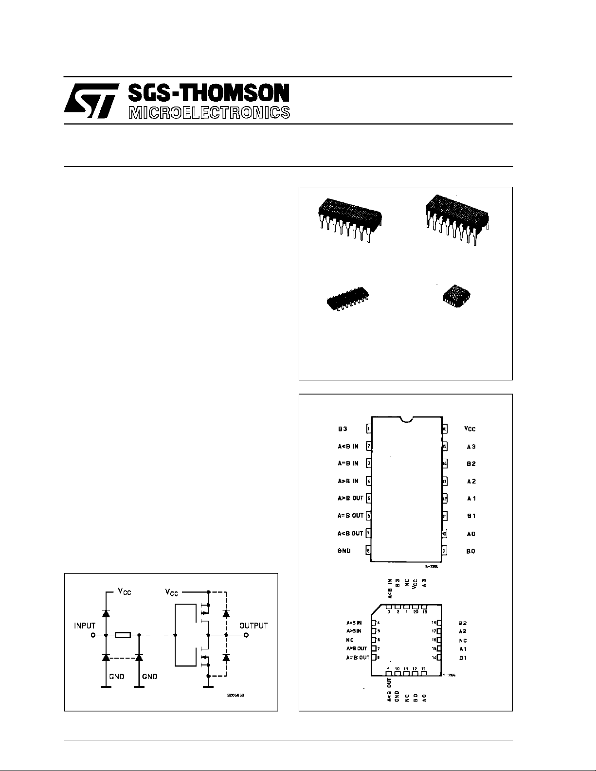
INPUT AND OUTPUT EQUIVALENT CIRCUIT
PIN CONNECTIONS(top view)
NC =
No Internal
Connection
December1992
1/11
Page 2
M54/M74HC85
PIN DESCRIPTION
PIN No SYMBOL NAME AND FUNCTION
2IN
3IN
4IN
5 OUT
6 OUT
7 OUT
9, 11, 14, 1 B
10, 12, 13, 15 A
0
0
A<B
A=B
A>B
to B
to A
A<B Expansion Input
A=B Expansion Input
A>B Expansion Input
A>B Expansion Output
A>B
A=B Expansion Output
A=B
A<B Expansion Output
A<B
Word B Inputs
3
Word A Inputs
3
8 GND Ground (0V)
16 V
CC
Positive Supply Voltage
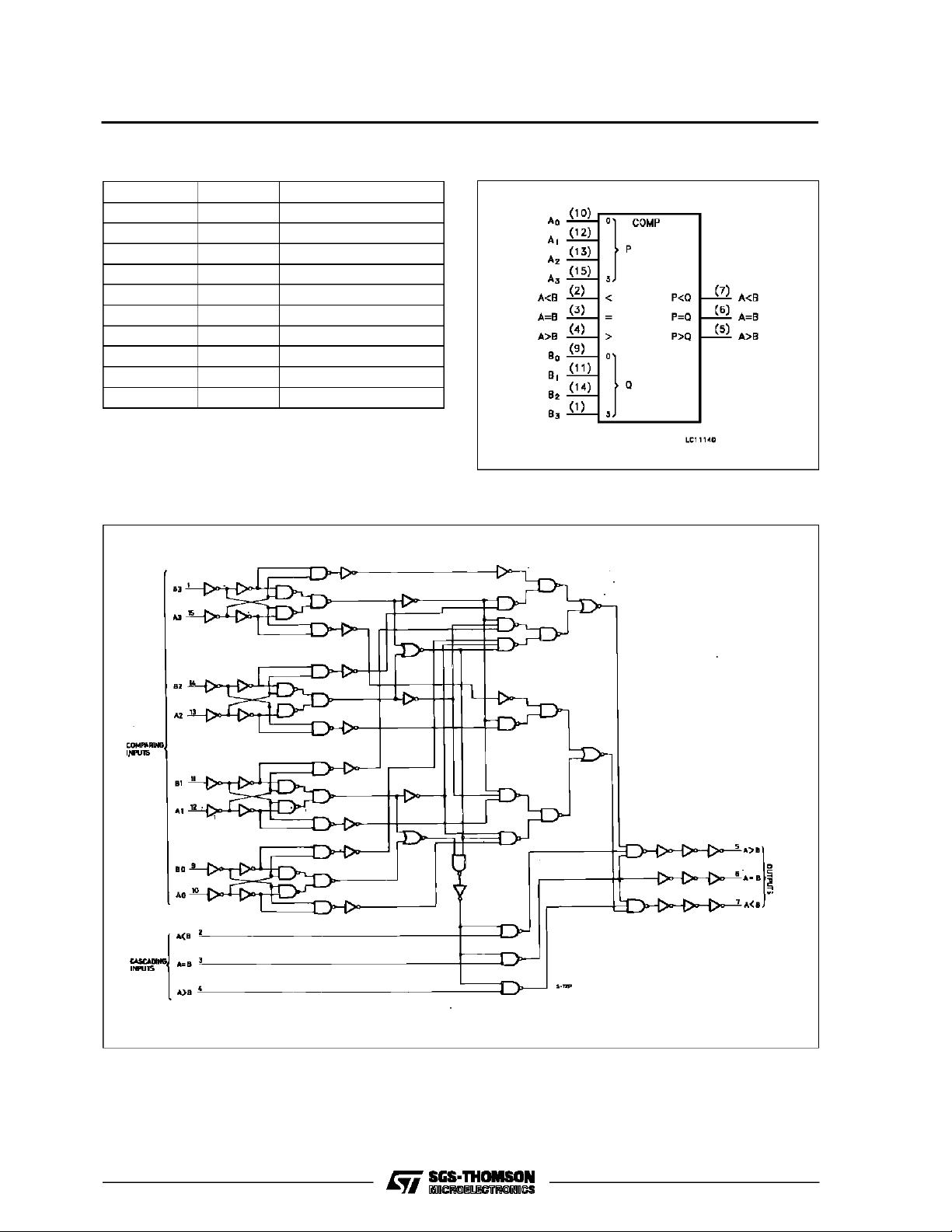
LOCIG DIAG RAM
IEC LOGIC SYMBOL
2/11
Page 3
TRUTH TABLE
M54/M74HC85
COMPARING INPUTS
CASCADING INPUTS OUTPUTS
A>B A<B A=B A>B A<B A=B
A3>B3 X X X X X X H L L
A3=B3 A2>B2 X X X X X H L L
A3=B3 A2=B2 A1>B1 X X X X H L L
A3=B3 A2=B2 A1=B1 A0>B0 X X X H L L
LLLHHL
XXHLLH
A3=B3 A2=B2 A1=B1 A0=B0
LHLLHL
HLLHLL
HHLLLL
A3=B3 A2=B2 A1=B1 A0<B0 X X X L H L
A3=B3 A2=B2 A1<B1 X X X X L H L
A3=B3 A2<B2 X X X X X L H L
A3<B3 X X X X X X L H L
X: DON’TCARE
ABSOLU TE M AXIMU M R AT INGS
Symbol Parameter Value Unit
V
CC
V
V
O
I
IK
I
OK
I
O
I
or I
CC
P
D
T
stg
T
L
AbsoluteMaximumRatingsarethose values beyondwhichdamagetothedevice mayoccur.Functionaloperationundertheseconditionisnotimplied.
(*)500 mW:≅ 65oC derate to300 mW by 10mW/oC: 65oCto85oC
Supply Voltage -0.5 to +7 V
DC Input Voltage -0.5 to VCC+ 0.5 V
I
DC Output Voltage -0.5 to VCC+ 0.5 V
DC Input Diode Current ± 20 mA
DC Output Diode Current ± 20 mA
DC Output Source Sink Current Per Output Pin ± 25 mA
DC VCCor Ground Current ± 50 mA
GND
Power Dissipation 500 (*) mW
Storage Temperature -65 to +150
Lead Temperature (10 sec) 300
o
C
o
C
3/11
Page 4
M54/M74HC85
RECO MM ENDED OPERAT I N G CO NDI TI O NS
Symbol Parameter Value Unit
V
V
V
T
t
r,tf
DC SPECIFICATIONS
Symbol Parameter
V
IH
V
V
OH
V
OL
I
I
CC
Supply Voltage 2 to 6 V
CC
Input Voltage 0 to V
I
Output Voltage 0 to V
O
Operating Temperature: M54HC Series
op
M74HC Series
CC
CC
-55 to +125
-40 to +85
Input Rise and Fall Time VCC= 2 V 0 to 1000 ns
V
= 4.5 V 0 to 500
CC
V
= 6 V 0 to 400
CC
Test Conditions Value
V
(V)
CC
=25oC
T
A
54HC and 74HC
-40 to 85oC
74HC
-55 to 125oC
Min. Typ. Max. Min. Max. Min. Max.
High Level Input
Voltage
2.0 1.5 1.5 1.5
4.5 3.15 3.15 3.15
6.0 4.2 4.2 4.2
Low Level Input
IL
Voltage
2.0 0.5 0.5 0.5
4.5 1.35 1.35 1.35
6.0 1.8 1.8 1.8
High Level
Output Voltage
Low Level Output
Voltage
Input Leakage
I
Current
Quiescent Supply
2.0
V
=
I
4.5 4.4 4.5 4.4 4.4
6.0 5.9 6.0 5.9 5.9
4.5 I
6.0 I
2.0
4.5 0.0 0.1 0.1 0.1
6.0 0.0 0.1 0.1 0.1
4.5 I
6.0 I
6.0
IO=-20 µA
V
IH
or
V
IL
=-4.0 mA 4.18 4.31 4.13 4.10
O
=-5.2 mA 5.68 5.8 5.63 5.60
O
V
=
I
IO=20µA
V
IH
or
V
IL
= 4.0 mA 0.17 0.26 0.33 0.40
O
= 5.2 mA 0.18 0.26 0.33 0.40
O
VI=VCCor GND ±0.1 ±1 ±1 µA
1.9 2.0 1.9 1.9
0.0 0.1 0.1 0.1
6.0 VI=VCCor GND 4 40 80 µA
Current
54HC
V
V
o
C
o
C
Unit
V
V
V
V
4/11
Page 5

M54/M74HC85
AC ELECTRICAL CHARACTERISTICS (CL=50pF,Inputtr=tf=6ns)
Test Conditions Value
T
=25oC
Symbol Parameter
t
t
TLH
THL
Output Transition
Time
V
CC
(V)
2.0 30 75 95 110
4.5 8151922
A
54HC and 74HC
Min. Typ. Max. Min. Max. Min. Max.
6.0 7131619
t
PLH
t
PHL
Propagation
Delay Time
(A, B-OUT)
t
t
PLH
PHL
Propagation
Delay Time
(CASCADE-OUT)
C
C
PD
Input Capacitance 5 10 10 10 pF
IN
(*) Power Dissipation
2.0 96 185 230 280
4.5 24 37 46 56
6.0 20 31 39 48
2.0 48 95 120 145
4.5 12 19 24 29
6.0 10 16 20 25
23
Capacitance
(*) CPDisdefinedas the value ofthe IC’s internal equivalent capacitance which is calculated fromthe operatingcurrent consumption withoutload.
(RefertoTest Circuit).Average opertingcurrentcan be obtained bythe followingequation. ICC(opr) = CPD•VCC•fIN+I
-40 to 85oC
74HC
-55 to 125oC
54HC
CC
Unit
ns
ns
ns
pF
SWITCHING CHARACTERISTICS TEST
WAVEFORM
TEST CIRCUIT ICC(Opr.)
INPUT WAVEFORM IS THE SAME AS THAT IN CASE OF
SWITCHINGCHARACTERISTICSTEST.
5/11
Page 6

M54/M74HC85
TYPICAL APPLICATION
LSB= lowestsignificantbit MSB= MOSTSIGNIFICANTBIT
X: DON’TCARE
COMPARING INPUTS
(A)>(B) X X X H L L
(A)=(B)
(A)<(B) X X X L L H
CASCADING INPUTS OUTPUTS
A>B A=B A<B A>B A=B A<B
HLLHLL
XHXLHL
LLHLLH
6/11
Page 7

Plastic DIP16 (0.25) MECHANICAL DATA
M54/M74HC85
DIM.
MIN. TYP. MAX. MIN. TYP. MAX.
a1 0.51 0.020
B 0.77 1.65 0.030 0.065
b 0.5 0.020
b1 0.25 0.010
D 20 0.787
E 8.5 0.335
e 2.54 0.100
e3 17.78 0.700
F 7.1 0.280
I 5.1 0.201
L 3.3 0.130
Z 1.27 0.050
mm inch
P001C
7/11
Page 8

M54/M74HC85
Ceramic DIP16/1 MECHANICAL DATA
DIM.
MIN. TYP. MAX. MIN. TYP. MAX.
A 20 0.787
B 7 0.276
D 3.3 0.130
E 0.38 0.015
e3 17.78 0.700
F 2.29 2.79 0.090 0.110
G 0.4 0.55 0.016 0.022
H 1.17 1.52 0.046 0.060
L 0.22 0.31 0.009 0.012
M 0.51 1.27 0.020 0.050
N 10.3 0.406
P 7.8 8.05 0.307 0.317
Q 5.08 0.200
mm inch
8/11
P053D
Page 9

SO16 (Narrow) MECHANICAL DATA
M54/M74HC85
DIM.
MIN. TYP. MAX. MIN. TYP. MAX.
A 1.75 0.068
a1 0.1 0.2 0.004 0.007
a2 1.65 0.064
b 0.35 0.46 0.013 0.018
b1 0.19 0.25 0.007 0.010
C 0.5 0.019
c1 45° (typ.)
D 9.8 10 0.385 0.393
E 5.8 6.2 0.228 0.244
e 1.27 0.050
e3 8.89 0.350
F 3.8 4.0 0.149 0.157
G 4.6 5.3 0.181 0.208
L 0.5 1.27 0.019 0.050
M 0.62 0.024
S8°(max.)
mm inch
P013H
9/11
Page 10

M54/M74HC85
PLCC20 MECHANICAL DATA
DIM.
MIN. TYP. MAX. MIN. TYP. MAX.
A 9.78 10.03 0.385 0.395
B 8.89 9.04 0.350 0.356
D 4.2 4.57 0.165 0.180
d1 2.54 0.100
d2 0.56 0.022
E 7.37 8.38 0.290 0.330
e 1.27 0.050
e3 5.08 0.200
F 0.38 0.015
G 0.101 0.004
M 1.27 0.050
M1 1.14 0.045
mm inch
10/11
P027A
Page 11

M54/M74HC85
Information furnished is believed to be accurate and reliable. However, SGS-THOMSON Microelectronics assumes no responsability for the
consequences of use of such information nor for any infringement of patents or other rights of third parties which may results from its use. No
license is grantedby implication or otherwise underany patent or patentrights ofSGS-THOMSON Microelectronics. Specificationsmentioned
in this publication are subject to change without notice. This publication supersedes and replaces all information previously supplied.
SGS-THOMSON Microelectronicsproductsare notauthorized foruse ascritical componentsin life supportdevices or systemswithout express
written approval of SGS-THOMSON Microelectonics.
1994 SGS-THOMSON Microelectronics - All Rights Reserved
Australia - Brazil - France - Germany - Hong Kong - Italy - Japan - Korea - Malaysia - Malta - Morocco - The Netherlands -
Singapore - Spain - Sweden - Switzerland - Taiwan - Thailand - UnitedKingdom - U.S.A
SGS-THOMSON Microelectronics GROUP OF COMPANIES
11/11
 Loading...