

Page 1
.HIGH SPEED
tPD= 10 ns(TYP.) AT VCC=5V
.LOWPOWERDISSIPATION
ICC=2µA(MAX.) AT TA=25°C
.HIGH NOISEIMMUNITY
V
NIH=VNIL
=28%VCC(MIN.)
.OUTPUT DRIVE CAPABILITY
10 LSTTL LOADS
.SYMMETRICALOUTPUT IMPEDANCE
IOH =IOL= 4 mA (MIN.)
.BALANCEDPROPAGATION DELAYS
t
PLH=tPHL
.WIDE OPERATINGVOLTAGE RANGE
VCC(OPR)= 2V TO6 V
.PIN AND FUNCTION COMPATIBLE WITH
54/74LS77
DESCRIPTION
The M54/74HC77 is a high speed CMOS 4-BIT DTYPELATCHfabricated in silicongateC2MOStechnology. It has the samehigh speed performance of
LSTTL combined with true CMOS low power consumption.It contains twogroups of 2-bit latches controlled by an enable input (G1• 2orG3•4). These
twolatch groups canbeusedindifferent circuits.The
dataapplied tothedata inputs(1D,2D,or3D,4D)are
transfered to the Q outputs (1Q,2Q, or 3Q, 4Q) respectively whentheenable input(G1 • 2orG3•4) is
takenhigh. The Q outputs will follow thedata inputs
aslong astheenableinputiskepthigh.Whenthe enableinput istaken low, theinformation dataapplied to
thedatainputs is retainedat theQ outputs. All inputs
areequipped withprotectioncircuitsagainst staticdischarge andtransient excess voltage.
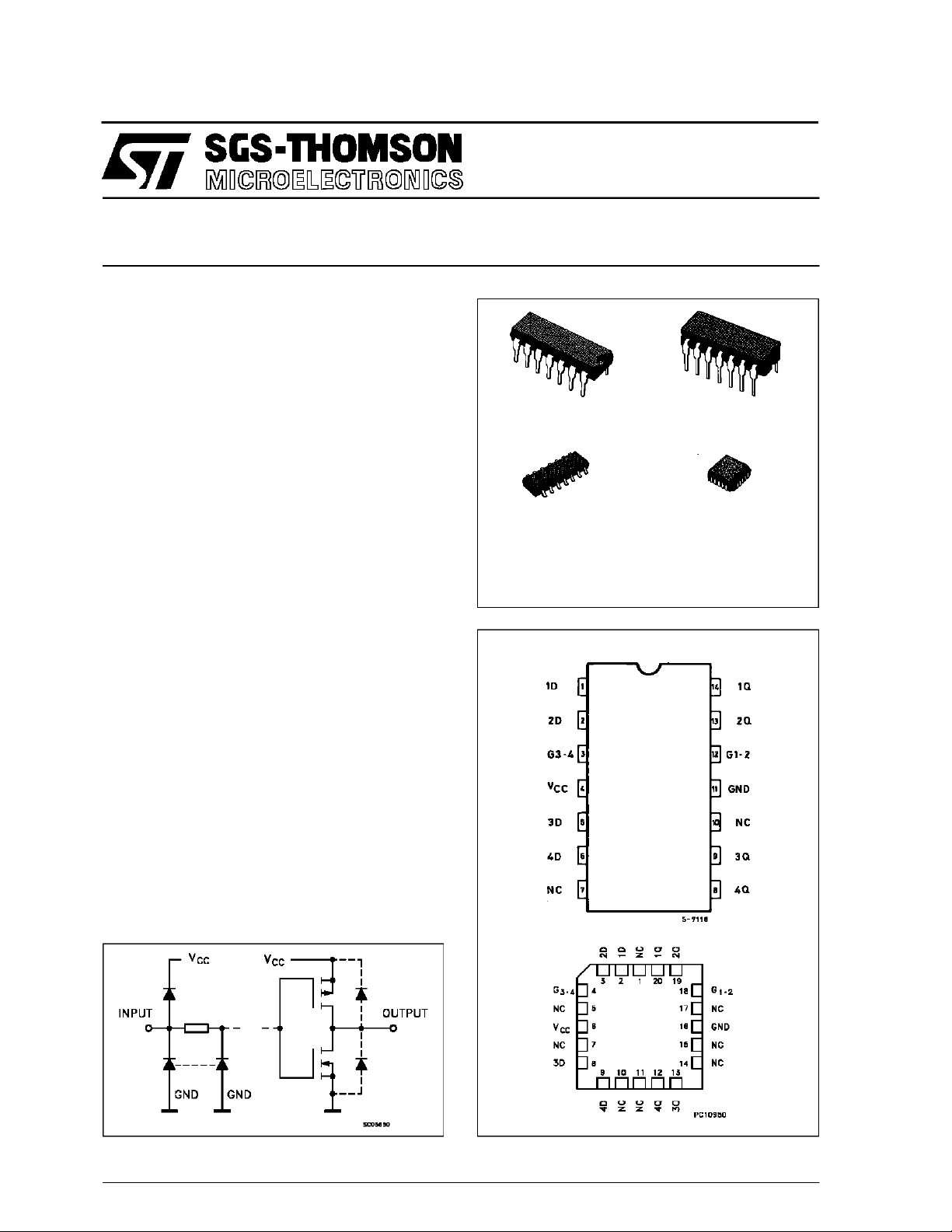
M54HC77
M74HC77
4-BIT D-TYPE LATCH
B1R
(PlasticPackage)
M1R
(MicroPackage)
ORDER CODES :
M54HC 77F1R M74H C77M1R
M74HC 77B1R M74HC7 7C1R
PIN CONNECTIONS(top view)
(CeramicPackage)
(Chip Carrier)
F1R
C1R
INPUT AND OUTPUT EQUIVALENT CIRCUIT
October 1992
NC =
No Internal
Connection
1/10
Page 2
M54/M74HC77
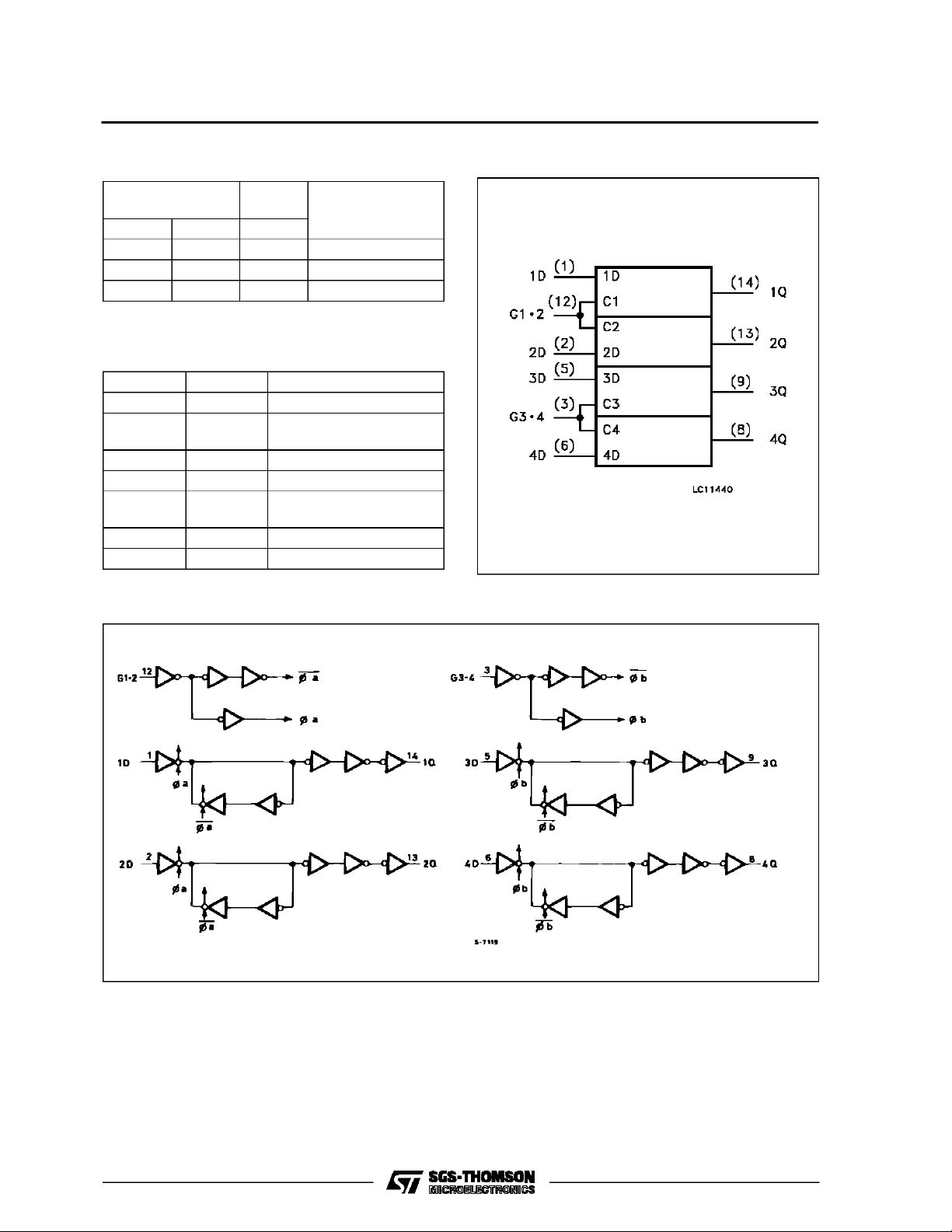
IEC LOGIC SYMBOLTRUTH TABLE
INPUTS
DGQ
LHL
HHH
XLQ
X:Don’t Care
OUTPUTS
n
FUNCTION
LATCH
PIN DESC RIPTION
PIN No SYMBOL NAME AND FUNCTION
1, 2, 5, 6 1D to 4D Data Inputs
3G3•4 Latch Enable Input,
Latches 3 and 4
7, 10 NC No Internal Connection
8, 9, 13, 14 1Q to 4Q Latch Outputs
12 G1 • 2 Latch Enable Input,
Latches 1 and 2
11 GND Ground (0V)
4V
CC
Positive Supply Voltage
LOGI C DI AGRAM
2/10
Page 3
M54/M74HC77
ABSOLU TE M AXIMU M R AT INGS
Symbol Parameter Value Unit
V
CC
V
V
O
I
IK
I
OK
I
O
I
or I
CC
P
D
T
stg
T
AbsoluteMaximumRatingsarethose valuesbeyond whichdamage to thedevice mayoccur.Functional operation under these conditionisnotimplied.
(*)500 mW: ≅ 65oC derateto300 mWby 10mW/oC: 65oCto85oC
RECO MM ENDED OPERATI N G CO NDI TI O NS
Symbol Parameter Value Unit
V
CC
V
I
V
O
T
op
t
r,tf
Supply Voltage -0.5 to +7 V
DC Input Voltage -0.5 to VCC+ 0.5 V
I
DC Output Voltage -0.5 to VCC+ 0.5 V
DC Input Diode Current ± 20 mA
DC Output Diode Current ± 20 mA
DC Output Source Sink Current Per Output Pin ± 25 mA
DC VCCor Ground Current ± 50 mA
GND
Power Dissipation 500 (*) mW
Storage Temperature -65 to +150
Lead Temperature (10sec) 300
L
Supply Voltage 2 to 6 V
Input Voltage 0 to V
Output Voltage 0 to V
Operating Temperature: M54HC Series
M74HC Series
CC
CC
-55 to +125
-40 to +85
Input Rise and Fall Time VCC= 2 V 0 to 1000 ns
V
= 4.5 V 0 to 500
CC
V
= 6 V 0 to 400
CC
o
C
o
C
V
V
o
C
o
C
3/10
Page 4

M54/M74HC77
DC SPECIFICATIONS
Symbol Parameter
V
V
V
V
I
High Level Input
IH
Voltage
Low Level Input
IL
Voltage
High Level
OH
Output Voltage
Low Level Output
OL
Voltage
I
Input Leakage
I
Current
Quiescent Supply
CC
Current
Test Conditions Value
V
(V)
CC
=25oC
A
54HC and 74HC
Min. Typ. Max. Min. Max. Min. Max.
-40 to 85oC
74HC
-55 to 125oC
54HC
Unit
T
2.0 1.5 1.5 1.5
4.5 3.15 3.15 3.15
6.0 4.2 4.2 4.2
2.0 0.5 0.5 0.5
4.5 1.35 1.35 1.35
6.0 1.8 1.8 1.8
2.0
4.5 4.4 4.5 4.4 4.4
6.0 5.9 6.0 5.9 5.9
4.5 I
6.0 I
2.0
4.5 0.0 0.1 0.1 0.1
6.0 0.0 0.1 0.1 0.1
4.5 I
6.0 I
6.0
=
V
I
IO=-20 µA
V
IH
or
V
IL
=-4.0 mA 4.18 4.31 4.13 4.10
O
=-5.2 mA 5.68 5.8 5.63 5.60
O
V
=
I
IO=20µA
V
IH
or
V
IL
= 4.0 mA 0.17 0.26 0.33 0.40
O
= 5.2 mA 0.18 0.26 0.33 0.40
O
VI=VCCor GND ±0.1 ±1 ±1 µA
1.9 2.0 1.9 1.9
0.0 0.1 0.1 0.1
6.0 VI=VCCor GND 2 20 40 µA
V
V
V
V
4/10
Page 5

M54/M74HC77
AC ELECTRICAL CHARACTERISTICS (CL=50pF,Inputtr=tf=6ns)
Test Conditions Value
T
=25oC
Symbol Parameter
t
t
TLH
THL
Output Transition
Time
V
CC
(V)
2.0 30 75 95 110
4.5 8151922
A
54HC and 74HC
Min. Typ. Max. Min. Max. Min. Max.
6.0 7131619
t
PLH
t
PHL
Propagation
Delay Time
(DATA - Q)
t
t
PLH
PHL
Propagation
Delay Time
(G - Q)
t
W(H)
Minimum Pulse
Width
(G)
Minimum Set-up
t
s
Time
2.0 39 100 125 150
4.5 13 20 25 30
6.0 11 17 21 26
2.0 39 100 125 150
4.5 13 20 25 30
6.0 11 17 21 26
2.0 15 75 95 110
4.5 6151922
6.0 6131619
2.0 15 50 65 75
4.5 3101315
6.0 3 9 11 13
t
h
Minimum Hold
Time
2.0 25 30 40
4.5 5 6 8
6.0 4 5 7
C
C
PD
Input Capacitance 5 10 10 10 pF
IN
(*) Power Dissipation
20
Capacitance
(*) CPDisdefined as the value ofthe IC’sinternal equivalent capacitance which is calculated fromthe operatingcurrent consumption without load.
(Referto Test Circuit). Average operting current canbe obtained bythe followingequation. ICC(opr) = CPD•VCC•fIN+ICC/4(per FLIP/FLOP)
-40 to 85oC
74HC
-55 to 125oC
54HC
Unit
ns
ns
ns
ns
ns
ns
pF
SWITCHING CHARACTERISTICS TEST
WAVEFORM
TEST CIRCUIT ICC(Opr)
INPUTWAVEFORMISTHESAVEASTHATINCASEOFSWITCHINGCHARACTERISTICSTEST.
5/10
Page 6

M54/M74HC77
Plastic DIP14 MECHANICAL DATA
DIM.
MIN. TYP. MAX. MIN. TYP. MAX.
a1 0.51 0.020
B 1.39 1.65 0.055 0.065
b 0.5 0.020
b1 0.25 0.010
D 20 0.787
E 8.5 0.335
e 2.54 0.100
e3 15.24 0.600
F 7.1 0.280
I 5.1 0.201
L 3.3 0.130
Z 1.27 2.54 0.050 0.100
mm inch
6/10
P001A
Page 7

Ceramic DIP14/1 MECHANICAL DATA
M54/M74HC77
DIM.
MIN. TYP. MAX. MIN. TYP. MAX.
A 20 0.787
B 7.0 0.276
D 3.3 0.130
E 0.38 0.015
e3 15.24 0.600
F 2.29 2.79 0.090 0.110
G 0.4 0.55 0.016 0.022
H 1.17 1.52 0.046 0.060
L 0.22 0.31 0.009 0.012
M 1.52 2.54 0.060 0.100
N 10.3 0.406
P 7.8 8.05 0.307 0.317
Q 5.08 0.200
mm inch
P053C
7/10
Page 8

M54/M74HC77
SO14 MECHANICAL DATA
DIM.
MIN. TYP. MAX. MIN. TYP. MAX.
A 1.75 0.068
a1 0.1 0.2 0.003 0.007
a2 1.65 0.064
b 0.35 0.46 0.013 0.018
b1 0.19 0.25 0.007 0.010
C 0.5 0.019
c1 45° (typ.)
D 8.55 8.75 0.336 0.344
E 5.8 6.2 0.228 0.244
e 1.27 0.050
e3 7.62 0.300
F 3.8 4.0 0.149 0.157
G 4.6 5.3 0.181 0.208
L 0.5 1.27 0.019 0.050
M 0.68 0.026
S8°(max.)
mm inch
8/10
P013G
Page 9

PLCC20 MECHANICAL DATA
M54/M74HC77
DIM.
MIN. TYP. MAX. MIN. TYP. MAX.
A 9.78 10.03 0.385 0.395
B 8.89 9.04 0.350 0.356
D 4.2 4.57 0.165 0.180
d1 2.54 0.100
d2 0.56 0.022
E 7.37 8.38 0.290 0.330
e 1.27 0.050
e3 5.08 0.200
F 0.38 0.015
G 0.101 0.004
M 1.27 0.050
M1 1.14 0.045
mm inch
P027A
9/10
Page 10

M54/M74HC77
Information furnishedis believed to be accurate and reliable. However, SGS-THOMSON Microelectronicsassumes no responsability for the
consequences of useof suchinformation nor for any infringement of patents or other rights of third parties which may results from its use. No
license is granted byimplication or otherwiseunder any patentor patentrights ofSGS-THOMSON Microelectronics.Specificationsmentioned
in this publication are subjectto changewithout notice. This publication supersedes andreplaces all information previouslysupplied.
SGS-THOMSON Microelectronicsproducts are not authorized foruse ascritical componentsin life supportdevices or systems without express
written approval of SGS-THOMSON Microelectonics.
1994SGS-THOMSON Microelectronics- All Rights Reserved
Australia -Brazil - France - Germany - Hong Kong - Italy - Japan - Korea - Malaysia - Malta -Morocco - The Netherlands-
Singapore -Spain - Sweden- Switzerland - Taiwan - Thailand- UnitedKingdom - U.S.A
SGS-THOMSON Microelectronics GROUP OFCOMPANIES
10/10
 Loading...