

Page 1
.HIGH SPEED
tPD= 10 ns (TYP.) AT VCC=5V
.LOWPOWER DISSIPATION
ICC=2 µA (MAX.) AT TA=25°C
.HIGH NOISEIMMUNITY
V
NIH=VNIL
=28%VCC(MIN.)
.OUTPUT DRIVE CAPABILITY
10 LSTTL LOADS
.SYMMETRICAL OUTPUT IMPEDANCE
IOH =IOL= 4 mA(MIN.)
.BALANCEDPROPAGATION DELAYS
t
PLH=tPHL
.WIDE OPERATINGVOLTAGERANGE
VCC=(OPR) = 2 V TO6 V
.PIN AND FUNCTION COMPATIBLE WITH
54/74LS75
DESCRIPTION
The M54/74HC75 is a high speed CMOS 4-BIT DTYPELATCHfabricated insilicongateC2MOStechnology. It has the same high speed performance of
LSTTL combined with true CMOS low power consumption.Itcontains twogroups of2-bit latchescontrolledbyanenableinput (G1•2orG3•4). These two
latch groups can be used in different circuits. Each
latch has Q and Q outputs (1Q - 4Q and 1Q - 4Q).
Thedata appliedto thedatainput istransferedto the
QandQ outputs whenthe enable input is takenhigh
and the outputs will follow the data input aslong as
the enableinputis kept high. When the enableinput
is takenlow,theinformation data applied tothe data
input is retained at the outputs. All inputs are
equipped with protection circuits against static discharge and transient excess voltage.
M54HC75
M74HC75
4 BIT D TYPE LATCH
B1R
(PlasticPackage)
M1R
(MicroPackage)
ORDER CODES :
M54HC 75F1R M74H C75M1R
M74HC 75B1R M 74HC75C1R
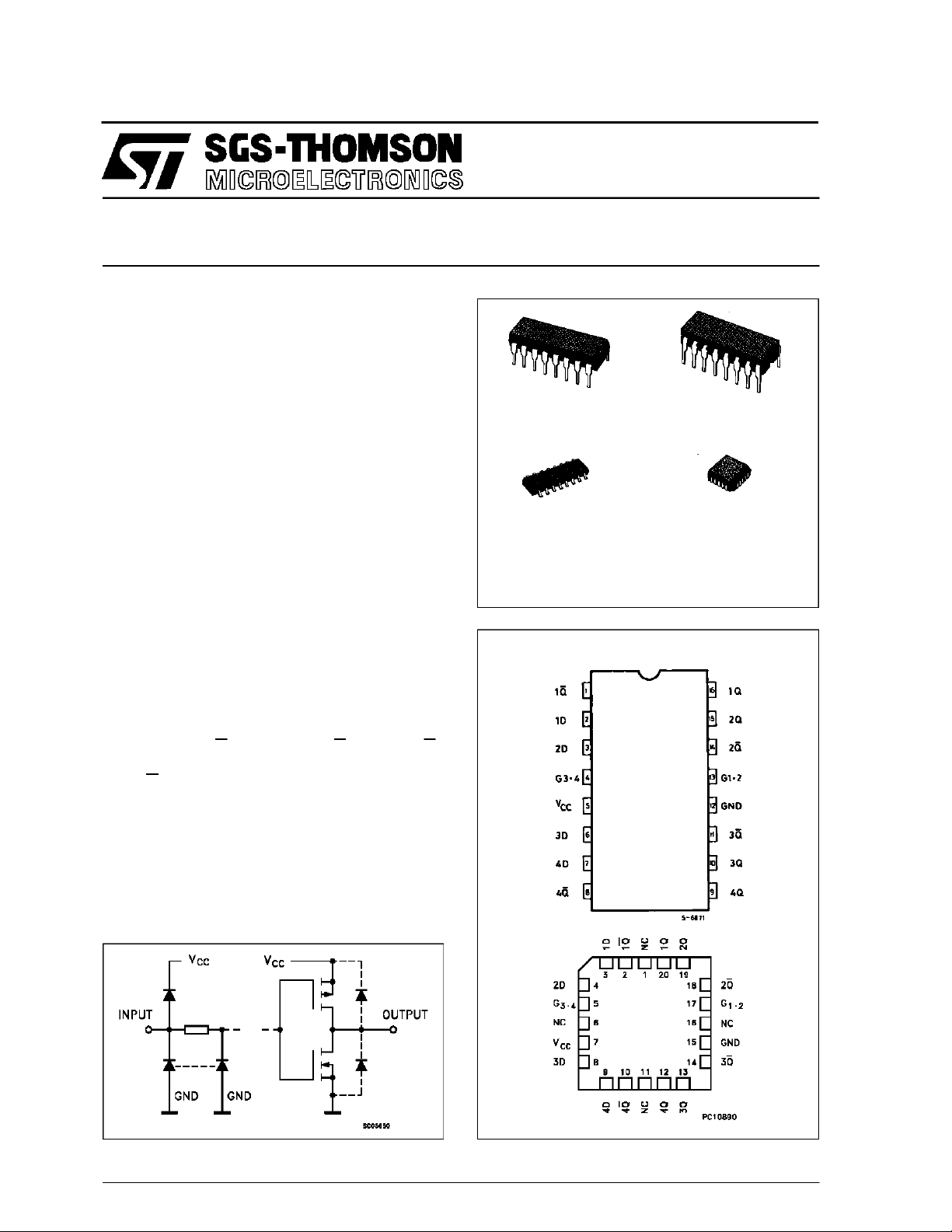
PIN CONNECTIONS(top view)
(CeramicPackage)
(Chip Carrier)
F1R
C1R
INPUT AND OUTPUT EQUIVALENT CIRCUIT
December1992
NC =
No Internal
Connection
1/9
Page 2
M54/M74HC75
TRUTH TABLE
INPUTS OUTPUTS
DGQQ
LHLH
HHHL
X L Qn Qn LATCH
FUNCTION
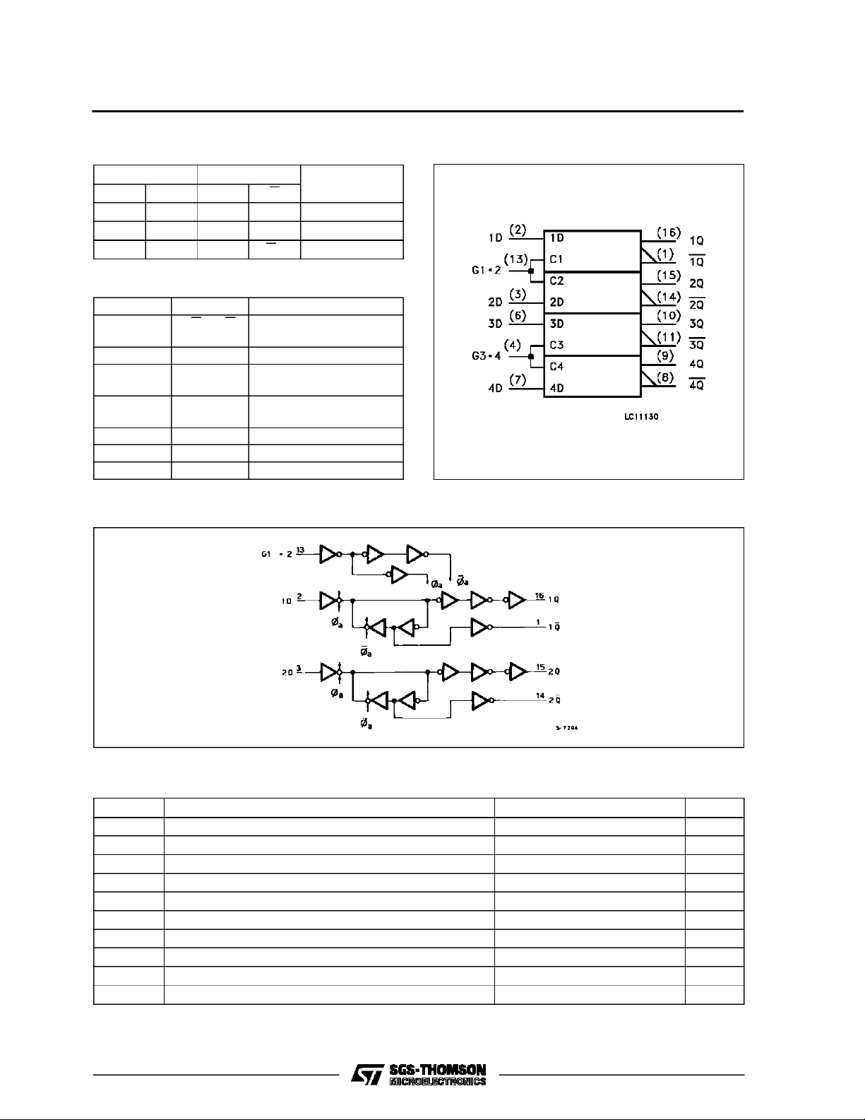
PIN DESCRIPTION
PIN No SYMBOL NAME AND FUNCTION
1, 14, 11, 8 1Q to 4Q Complementary Latch
Outputs
2, 3, 6, 7 1D to 4D Data Inputs
4G3•4 Latch Enable Input,
latches 3 and 4
13 G1 • 2 Latch Enable Input,
latches 1 and 2
16, 15, 10, 9 1Q to 4Q Latch Outputs
12 GND Ground (0V)
5V
CC
Positive Supply Voltage
SCHEM ATIC C I R CUI T
IEC LOGIC SYMBOL
ABSOLU TE MAXIMU M RAT INGS
Symbol Parameter Value Unit
V
CC
V
V
O
I
IK
I
OK
I
O
I
or I
CC
P
D
T
stg
T
L
AbsoluteMaximumRatingsarethose values beyondwhichdamage tothedevicemayoccur.Functional operationunder theseconditionisnotimplied.
(*)500 mW: ≅ 65oC derate to300 mW by 10mW/oC: 65oCto85oC
2/9
Supply Voltage -0.5 to +7 V
DC Input Voltage -0.5 to VCC+ 0.5 V
I
DC Output Voltage -0.5 to VCC+ 0.5 V
DC Input Diode Current ± 20 mA
DC Output Diode Current ± 20 mA
DC Output Source Sink Current Per Output Pin ± 25 mA
DC VCCor Ground Current ± 50 mA
GND
Power Dissipation 500 (*) mW
Storage Temperature -65 to +150
Lead Temperature (10 sec) 300
o
C
o
C
Page 3
M54/M74HC75
RECO MM ENDED OPERATI N G CONDI TI O NS
Symbol Parameter Value Unit
V
V
V
T
t
r,tf
DC SPECIFICA TIONS
Symbol Parameter
V
IH
V
V
OH
V
OL
I
I
CC
Supply Voltage 2 to 6 V
CC
Input Voltage 0 to V
I
Output Voltage 0 to V
O
Operating Temperature: M54HC Series
op
M74HC Series
CC
CC
-55 to +125
-40 to +85
Input Rise and Fall Time VCC= 2 V 0 to 1000 ns
V
= 4.5 V 0 to 500
CC
V
= 6 V 0 to 400
CC
Test Conditions Value
V
(V)
CC
=25oC
T
A
54HC and 74HC
-40 to 85oC
74HC
-55 to 125oC
Min. Typ. Max. Min. Max. Min. Max.
High Level Input
Voltage
2.0 1.5 1.5 1.5
4.5 3.15 3.15 3.15
6.0 4.2 4.2 4.2
Low Level Input
IL
Voltage
2.0 0.5 0.5 0.5
4.5 1.35 1.35 1.35
6.0 1.8 1.8 1.8
High Level
Output Voltage
Low Level Output
Voltage
Input Leakage
I
Current
Quiescent Supply
2.0
V
=
I
4.5 4.4 4.5 4.4 4.4
6.0 5.9 6.0 5.9 5.9
4.5 I
6.0 I
2.0
4.5 0.0 0.1 0.1 0.1
6.0 0.0 0.1 0.1 0.1
4.5 I
6.0 I
6.0
IO=-20 µA
V
IH
or
V
IL
=-4.0 mA 4.18 4.31 4.13 4.10
O
=-5.2 mA 5.68 5.8 5.63 5.60
O
V
=
I
IO=20µA
V
IH
or
V
IL
= 4.0 mA 0.17 0.26 0.33 0.40
O
= 5.2 mA 0.18 0.26 0.33 0.40
O
VI=VCCor GND ±0.1 ±1 ±1 µA
1.9 2.0 1.9 1.9
0.0 0.1 0.1 0.1
6.0 VI=VCCor GND 2 20 40 µA
Current
54HC
V
V
o
C
o
C
Unit
V
V
V
V
3/9
Page 4

M54/M74HC75
AC ELECTRICAL CHARACTERISTICS (CL=50pF,Inputtr=tf=6ns)
Test Conditions Value
T
=25oC
Symbol Parameter
t
t
TLH
THL
Output Transition
Time
V
CC
(V)
2.0 25 75 95 110
4.5 7151922
A
54HC and 74HC
Min. Typ. Max. Min. Max. Min. Max.
6.0 6131619
t
PLH
t
PHL
Propagation
Delay Time
(DATA-Q)
t
t
PLH
PHL
Propagation
Delay Time
(G-Q)
t
W(H)
Minimum Pulse
Width (G)
2.0 36 110 140 165
4.5 12 22 28 33
6.0 10 19 24 28
2.0 40 125 155 190
4.5 13 25 31 38
6.0 11 21 26 32
2.0 18 75 95 110
4.5 6151922
6.0 6131619
Minimum Set-up
t
s
Time
2.0 50 65 75
4.5 10 13 15
6.0 9 11 13
t
h
Minimum Hold
Time
2.0 25 30 40
4.5 5 6 8
6.0 4 5 7
C
C
PD
Input Capacitance 5 10 10 10 pF
IN
(*) Power Dissipation
30
Capacitance
(*) CPDisdefinedas the value ofthe IC’sinternal equivalent capacitance which is calculated fromthe operatingcurrent consumption without load.
(RefertoTestCircuit).Average opertingcurrent can be obtained bythe followingequation. ICC(opr) = CPD•VCC•fIN+I
-40 to 85oC
74HC
-55 to 125oC
54HC
CC
Unit
ns
ns
ns
ns
ns
ns
pF
SWITCHING CHARACTERISTICS TEST
WAVEFORM
4/9
TEST CIRCUIT ICC(Opr)
* INPUT WAVEFORM IS THE SAVE AS THAT IN CASE OF
SWITCHINGCHARACTERISTICSTEST.
Page 5

Plastic DIP16 (0.25) MECHANICAL DATA
M54/M74HC75
DIM.
MIN. TYP. MAX. MIN. TYP. MAX.
a1 0.51 0.020
B 0.77 1.65 0.030 0.065
b 0.5 0.020
b1 0.25 0.010
D 20 0.787
E 8.5 0.335
e 2.54 0.100
e3 17.78 0.700
F 7.1 0.280
I 5.1 0.201
L 3.3 0.130
Z 1.27 0.050
mm inch
P001C
5/9
Page 6

M54/M74HC75
Ceramic DIP16/1 MECHANICAL DATA
DIM.
MIN. TYP. MAX. MIN. TYP. MAX.
A 20 0.787
B 7 0.276
D 3.3 0.130
E 0.38 0.015
e3 17.78 0.700
F 2.29 2.79 0.090 0.110
G 0.4 0.55 0.016 0.022
H 1.17 1.52 0.046 0.060
L 0.22 0.31 0.009 0.012
M 0.51 1.27 0.020 0.050
N 10.3 0.406
P 7.8 8.05 0.307 0.317
Q 5.08 0.200
mm inch
6/9
P053D
Page 7

SO16 (Narrow) MECHANICAL DATA
M54/M74HC75
DIM.
MIN. TYP. MAX. MIN. TYP. MAX.
A 1.75 0.068
a1 0.1 0.2 0.004 0.007
a2 1.65 0.064
b 0.35 0.46 0.013 0.018
b1 0.19 0.25 0.007 0.010
C 0.5 0.019
c1 45° (typ.)
D 9.8 10 0.385 0.393
E 5.8 6.2 0.228 0.244
e 1.27 0.050
e3 8.89 0.350
F 3.8 4.0 0.149 0.157
G 4.6 5.3 0.181 0.208
L 0.5 1.27 0.019 0.050
M 0.62 0.024
S8°(max.)
mm inch
P013H
7/9
Page 8

M54/M74HC75
PLCC20 MECHANICAL DATA
DIM.
MIN. TYP. MAX. MIN. TYP. MAX.
A 9.78 10.03 0.385 0.395
B 8.89 9.04 0.350 0.356
D 4.2 4.57 0.165 0.180
d1 2.54 0.100
d2 0.56 0.022
E 7.37 8.38 0.290 0.330
e 1.27 0.050
e3 5.08 0.200
F 0.38 0.015
G 0.101 0.004
M 1.27 0.050
M1 1.14 0.045
mm inch
8/9
P027A
Page 9

M54/M74HC75
Information furnished is believed to be accurate and reliable. However, SGS-THOMSON Microelectronics assumes no responsability for the
consequences of use of such information nor for any infringement of patents or other rights of third parties which may results from its use. No
license is grantedbyimplication or otherwise under any patent or patentrights ofSGS-THOMSON Microelectronics. Specificationsmentioned
in this publication are subject to change without notice. This publication supersedes and replaces all information previously supplied.
SGS-THOMSON Microelectronicsproductsare notauthorized foruse ascriticalcomponentsinlife support devices orsystems withoutexpress
written approval of SGS-THOMSON Microelectonics.
1994 SGS-THOMSON Microelectronics - All Rights Reserved
Australia - Brazil - France - Germany - Hong Kong - Italy - Japan - Korea - Malaysia - Malta - Morocco - The Netherlands -
Singapore - Spain - Sweden - Switzerland - Taiwan - Thailand - UnitedKingdom - U.S.A
SGS-THOMSON Microelectronics GROUP OF COMPANIES
9/9
 Loading...