

Datasheet M74HC7294, M74HC7292, M74HC294, M74HC292 Datasheet (SGS Thomson Microelectronics)
Page 1
PROGRAMMABLE DIVIDER/TIMER
.HIGH SPEED
f
= 70 MHz(TYP.) at VCC=5V
MAX
.LOWPOWERDISSIPATION
ICC=4 mA(MAX.) at TA=25oC
.HIGH NOISEIMMUNITY
V
NIH=VNIL
=28%VCC(MIN.)
.OUTPUT DRIVECAPABILITY
10 LSTTL LOADS
.SYMMETRICALOUTPUT IMPEDANCE
|IOH|=IOL=4 mA(MIN.)
.BALANCEDPROPAGATION DELAYS
t
PLH=tPHL
.WIDE OPERATINGVOLTAGERANGE
VCC(OPR)= 2V TO 6 V
.PIN AND FUNCTION COMPATIBLE WITH
54/74LS292/294
DESCRIPTION
The 54/74HC292/7292 and HC294/7294 are high
speedCMOS PROGRAMMABLEDIVIDER/TIMER
fabricated with silicon C2MOStechnology.
They achieve the high speed operation similar to
equivalent LSTTL while maintaining the CMOSlow
power dissipation.
These devices are programmable frequency
dividers. Thetypeshavetwoclockinputs,eitherone
may be used for clock gating. (see the function
table). The HC292/7292 can divide from 22to 231,
and theHC294/7294 can divide from22to215. The
M54/74HC292/7292
M54/74HC294/7294
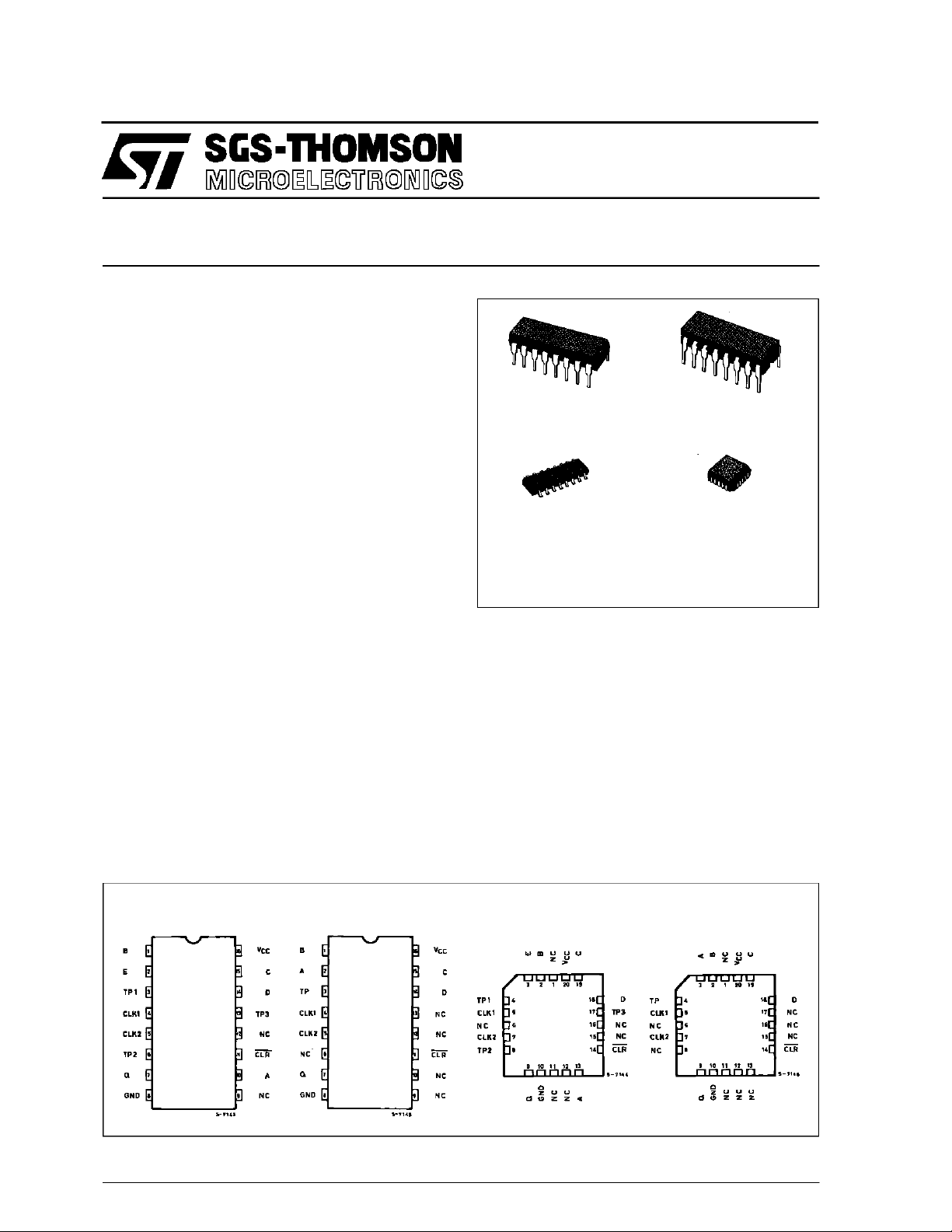
B1R
(PlasticPackage)
M1R
(MicroPackage)
ORDER CODES :
M54HC X XXF1R M74HC XXXM1R
M74HC X XXB1R M74H CXXXC1R
types feature an active-low clear input to initialize
the state of all flip-flops. To facilitate incoming
inspection, test points are provided. (TP1, TP2 and
TP3 on the HC292/7292 and TP on the
HC294/7294). All inputs are equipped with
protection circuits against static discharge and
transient excess voltage.
HC292/294 have Q output with ”Totem pole”
configuration and test point TP with ”Open Drain”
outputconfiguration.
HC7292/7294 have all outputs ”Totem Pole”.
F1R
(CeramicPackage)
C1R
(Chip Carrier)
PIN CONNECTION (top view)
HC292
HC7292
October 1993
HC294
HC7294
HC292
HC7292
HC294
HC7294
1/14
Page 2
M54/M74HC292/7292/294/7294
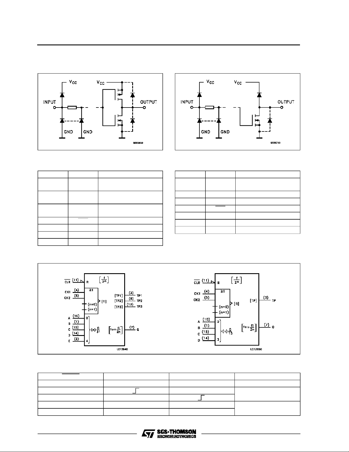
INPUT AND OUTPUT EQUIVALENT CIRCUIT
(TOTEM POLE OUTPUT)
PIN DESC RIPTION (HC292/7292)
PIN No SYMBOL NAME AND FUNCTION
4, 5 CLK1,
CLK2
1, 2, 10,
14, 15
3, 6, 13 TP1, TP2,
11 CLR Clear (Active LOW)
7 Q Output
8 GND Ground (0V)
16 V
A to E Program Inputs
TP3
CC
input Clock
Test Point Outputs
Positive Supply Voltage
INPUT AND OUTPUT EQUIVALENT CIRCUIT
(OPEN DRAIN OUTPUT, HC292/294)
PIN DESCRIPTION ( HC294/ 7294)
PIN No SYMBOL NAME AND FUNCTION
4, 5 CLK1,
CLK2
1, 2, 14, 15 A to D Program Inputs
3 TP1 Test Point Output
11 CLR Clear (Active LOW)
7 Q Output
8 GND Ground (0V)
16 V
CC
input Clock
Positive Supply Voltage
IEC LOGIC SYMBOLS
HC292/HC7292 HC294/HC7294
TRUTH TABLE
CLEAR CLOCK1 CLOCK2 Q OUTPUT MODE
L X X CLEARED TO L
H L UP COUNT
HL
H H X NO CHANGE
HXH
2/14
Page 3
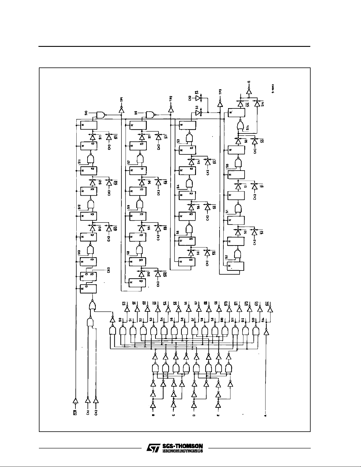
LOGIC DIAGRAM (HC292/7292)
M54/M74HC292/7292/294/7294
3/14
Page 4
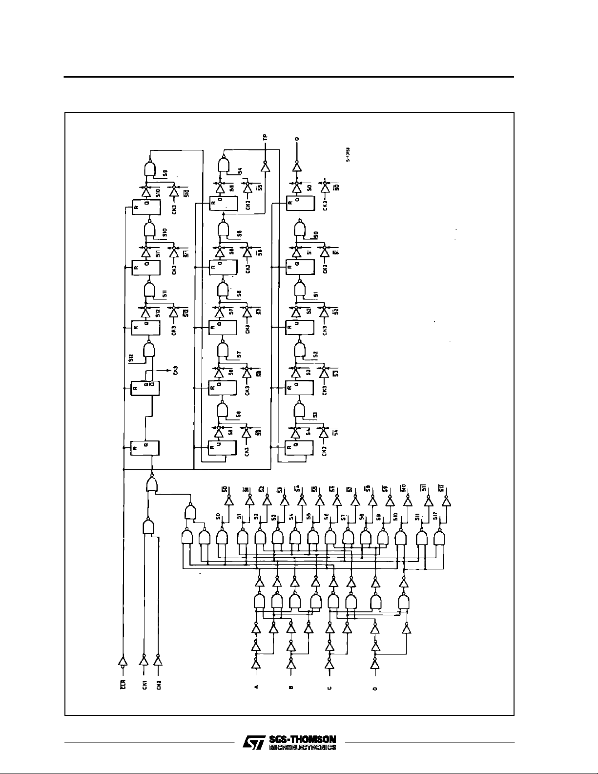
M54/M74HC292/7292/294/7294
LOGIC DIAGRAM (HC294/7294)
4/14
Page 5
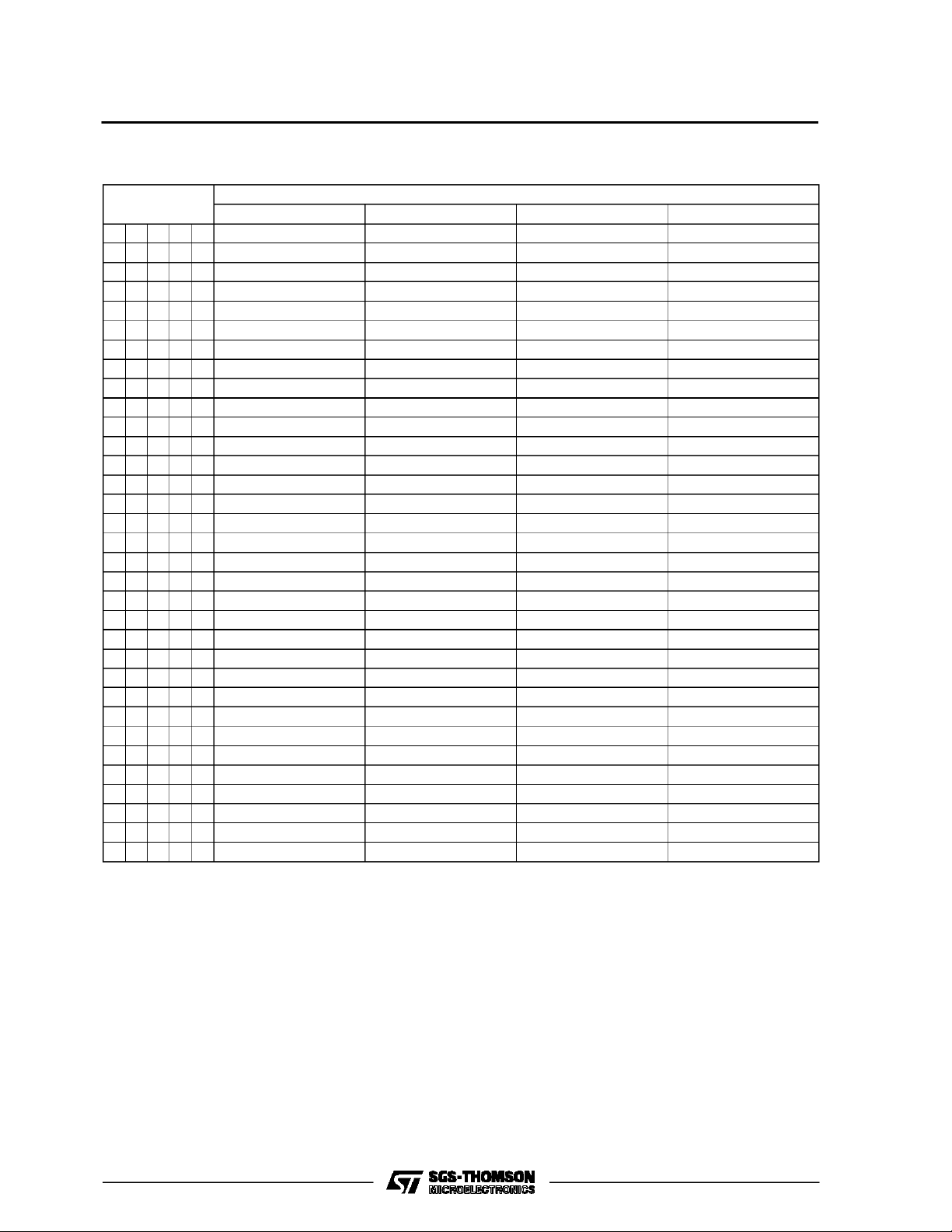
FUNCTION TABLE (HC292/7292)
M54/M74HC292/7292/294/7294
PROGRA MMI NG
INPUTS
Q TP1 TP2 TP3
FREQUENCY DIVISION
E D C B A BINARY DECIMAL BINARY DECIMAL BINARY DECIMAL BINARY DECIMAL
L L L L L Inhibit Inhibit Inhibit Inhibit Inhibit Inhibit Inhibit Inhibit
L L L L H Inhibit Inhibit Inhibit Inhibit Inhibit Inhibit Inhibit Inhibit
LLLHL2
LLLHH2
LLHLL2
LLHLH2
LLHHL2
LLHHH2
LHLLL2
LHLLH2
LHLHL2
LHLHH2
LHHLL2
LHHLH2
LHHHL2
HHHHH2
HLLLL2
HLLLH2
HLLHL2
HLLHH2
HLHLL2
HLHLH2
HLHHL2
HLHHH2
HHLLL2
HHLLH2
HHLHL2
HHLHH2
HHHLL2
HHHLH2
HHHHL2
HHHHH2
2
3
4
5
6
7
8
9
10
11
12
13
14
15
16
17
18
19
20
21
22
23
24
25
26
27
28
29
30
31
128 2
256 2
512 2
1,024 2
2,048 2
4,096 2
8,192 2
16,384 2
32,768 2
65,536 2
131,072 2
262,144 2
524,288 2
1,048,576 2
2,097,152 2
4,194,304 Disabled Low 2
8,388,608 Disabled Low 2
16,777,216 2
33,554,432 2
67,108,864 2
134,217,728 2
268,435,456 2
536,870,912 2
1,073,741,824 2
2,147,483,648 2
42
82
16 2
32 2
64 2
9
9
9
9
9
9
9
9
9
9
9
9
9
9
9
9
9
9
9
9
3
3
5
5
7
7
9
9
512 2
512 2
512 2
512 2
512 2
512 2
512 2
512 2
512 2
512 2
512 2
512 2
17
17
17
17
17
17
17
17
17
17
17
17
131,072 2
131,072 2
131,072 2
131,072 2
131,072 2
131,072 2
131,072 2
131,072 2
131,072 2
131,072 2
131,072 2
131,072 2
512 Disabled Low 2
512 Disabled Low 2
512 2
512 2
512 2
512 2
512 2
512 2
128 2
128 2
512 2
512 2
82
82
32 2
32 2
3
3
5
5
7
7
9
9
11
11
13
13
15
15
17
17
82
82
32 2
32 2
128 2
128 2
512 2
512 2
2,048 2
2,048 2
8,192 2
8,192 2
32,768 2
32,768 2
131,072 2
131,072 2
24
24
24
24
24
24
2
2
4
4
6
6
8
8
10
10
12
12
14
14
16
16
18
18
20
20
22
22
24
24
16,777,216
16,777,216
16,777,216
16,777,216
16,777,216
16,777,216
4
4
16
16
64
64
256
256
1,024
1,024
4,096
4,096
16,384
16,384
65,536
65,536
262,144
262,144
1,048,576
1,048,576
4,194,304
4,194,304
16,777,216
16,777,216
5/14
Page 6

M54/M74HC292/7292/294/7294
FUNCTION TABLE (HC294/7294)
PROGRAMMIN G
INPUTS
QTP
FREQUENCY DIVISION
D C B A BINARY DECIMAL BINARY DECIMAL
L L L L Inhibit Inhibit Inhibit Inhibit
L L L H Inhibit Inhibit Inhibit Inhibit
LLHL2
LLHH2
LHLL2
LHLH2
LHHL2
LHHH2
HLLL2
HLLH2
HLHL2
HLHH2
HHLL2
HHLH2
HHHL2
HHHH2
2
3
4
5
6
7
8
9
10
11
12
13
14
15
16 2
32 2
64 2
128 Disabled Low
256 2
512 2
1,024 2
2,048 2
4,096 2
8,192 2
16,384 2
32,768 2
9
42
9
82
9
9
9
2
3
4
5
6
7
8
9
512
512
512
512
512
4
8
16
32
64
128
256
512
ABSOLU TE MAXI MU M RAT I NG S
Symbol Parameter Value Unit
V
CC
V
V
O
I
IK
I
OK
I
O
I
or I
CC
P
D
T
stg
T
AbsoluteMaximum Ratings arethosevalues beyond whichdamagetothedevicemayoccur.Functionaloperationunder theseconditions is notimplied.
(*)500 mW: ≅ 65oC derateto300mWby 10mW/oC: 65oCto85oC
Supply Voltage -0.5 to +7 V
DC Input Voltage -0.5 to VCC+ 0.5 V
I
DC Output Voltage -0.5 to VCC+ 0.5 V
DC Input Diode Current ± 20 mA
DC Output Diode Current ± 20 mA
DC Output Source Sink Current Per Output Pin ± 25 mA
DC VCCor Ground Current ± 50 mA
GND
Power Dissipation 500 (*) mW
Storage Temperature -65 to +150
Lead Temperature (10 sec) 300
L
o
C
o
C
RECO MM ENDED OPERAT IN G CO NDI TI O NS
Symbol Parameter Value Unit
6/14
V
T
t
V
V
r,tf
Supply Voltage 2 to 6 V
CC
Input Voltage 0 to V
I
Output Voltage 0 to V
O
Operating Temperature: M54HC Series
op
M74HC Series
CC
CC
-55 to +125
-40 to +85
Input Rise and Fall Time VCC= 2 V 0 to 1000 ns
= 4.5 V 0 to 500
V
CC
V
= 6 V 0 to 400
CC
V
V
o
C
o
C
Page 7

DC SPECIFICATIONS
Symbol Parameter
V
V
V
V
V
V
I
High Level Input
IH
Voltage
Low Level Input
IL
Voltage
High Level
OH
Output Voltage
(Q)
High Level
OH
Output Voltage
(TP) (for HC7292
HC7294 only)
Low Level Output
OL
Voltage
(Q)
Low Level Output
OL
Voltage
(TP)
I
Input Leakage
I
Current
Quiescent Supply
CC
Current
M54/M74HC292/7292/294/7294
Test Conditions Value
T
=25oC
V
(V)
CC
A
54HC and 74HC
Min. Typ. Max. Min. Max. Min. Max.
2.0 1.5 1.5 1.5
4.5 3.15 3.15 3.15
6.0 4.2 4.2 4.2
2.0 0.5 0.5 0.5
4.5 1.35 1.35 1.35
6.0 1.8 1.8 1.8
2.0
4.5 4.4 4.5 4.4 4.4
6.0 5.9 6.0 5.9 5.9
4.5 I
6.0 I
2.0
4.5 4.4 4.5 4.4 4.4
6.0 5.9 6.0 5.9 5.9
4.5 I
6.0 I
2.0
4.5 0.0 0.1 0.1 0.1
6.0 0.0 0.1 0.1 0.1
4.5 I
6.0 I
2.0
4.5 0.0 0.1 0.1 0.1
6.0 0.0 0.1 0.1 0.1
4.5 I
6.0 I
6.0
=
V
I
IO=-20 µA
V
IH
or
V
IL
=-4.0 mA 4.18 4.31 4.13 4.10
O
=-5.2 mA 5.68 5.8 5.63 5.60
O
V
=
I
IO=-20 µA
V
IH
or
V
IL
=-1.0 mA 4.18 4.31 4.13 4.10
O
=-1.3 mA 5.68 5.8 5.63 5.60
O
=
V
I
IO=20µA
V
IH
or
V
IL
= 4.0 mA 0.17 0.26 0.33 0.40
O
= 5.2 mA 0.18 0.26 0.33 0.40
O
=
V
I
IO=20µA
V
IH
or
V
IL
= 1.0 mA 0.17 0.26 0.33 0.40
O
= 1.3 mA 0.18 0.26 0.33 0.40
O
VI=VCCor GND ±0.1 ±1 ±1 µA
1.9 2.0 1.9 1.9
1.9 2.0 1.9 1.9
0.0 0.1 0.1 0.1
0.0 0.1 0.1 0.1
6.0 VI=VCCor GND 4 40 80 µA
-40 to 85oC
74HC
-55 to 125oC
54HC
Unit
V
V
V
V
V
V
7/14
Page 8

M54/M74HC292/7292/294/7294
AC ELECTRICAL CHARACTERISTICS (CL=50pF,Inputtr=tf=6ns)
Test Conditions Value
=25oC
T
Symbol Parameter
t
t
TLH
THL
Output Transition
Time
(Q)
t
TLH
t
THL
Output Transition
Time
(TP)
t
t
PLH
PHL
Propagation
Delay Time
(CK - Q)
t
t
PLH
PHL
Propagation
Delay Time
(CK - Q)
t
PHL
Propagation
Delay Time
(CLR - Q)
t
PHL
Propagation
Delay Time
(CLR - Q)
f
MAX
Maximum Clock
Frequency
V
CC
(V)
2.0 30 75 95 110
4.5 8151922
6.0 7131619
2.0 116 225 280 340
4.5 29 45 56 68
6.0 25 38 48 57
2.0
for HC292/7292
4.5 46 70 88 105
6.0 39 60 75 90
2.0
for HC294/7294
4.5 43 66 83 15
6.0 37 56 71 84
2.0
for HC292/7292
4.5 42 64 80 100
6.0 36 54 68 81
2.0
for HC294/7294
4.5 34 52 65 78
6.0 29 44 55 66
2.0
for HC292/7292
4.5 27 64 22 18
A
54HC and 74HC
Min. Typ. Max. Min. Max. Min. Max.
160 350 440 ns
145 330 415
130 320 400 210
110 260 325 390
5.0 21 4 3.4
6.0 32 75 26 21
f
MAX
Maximum Clock
Frequency
2.0
for HC294/7294
4.5 32 64 26 21
6.0 20 5 4
6.0 38 75 31 25
t
W(H)
t
W(L)
t
W(L)
t
W(L)
t
REM
Minimum Pulse
Width
(CLOCK)
Minimum Pulse
Width
(CLEAR)
Minimum Pulse
Width
(CLEAR)
Minimum
Removal Time
2.0 40 75 95 110
4.5 8151922
6.0 7131620
2.0
for HC292/7292
4.5 12 25 31 38
48 125 155 190
6.0 10 21 26 32
2.0
for HC294/7294
4.5 10 20 25 30
40 100 125 150
6.0 9172126
2.0
for HC292/7292
4.5 5 5 5
6.0 5 5 5
t
REM
Minimum
Removal Time
2.0
for HC294/7294
4.5 0 0 0
6.0 0 0 0
C
C
PD
(*) CPDisdefined asthe valueofthe IC’s internal equivalent capacitance which iscalculated from theoperating current consumption without load.
(RefertoTest Circuit).Average operting current canbeobtained by the followingequation. ICC(opr) = CPD•VCC•fIN+I
Input Capacitance 5 10 10 pF
IN
(*) Power Dissipation
Capacitance
for HC292/7292
for HC294/7294
21
23
-40 to 85oC
74HC
-55 to 125oC
54HC
Unit
ns
ns
ns
ns
ns
MHz
MHz
ns
ns
ns
555
ns
000
ns
pF
CC
8/14
Page 9

SWITCHING CHARACTERISTICS TEST WAVEFORM
M54/M74HC292/7292/294/7294
TEST CIRCUIT ICC(Opr.)
HC292/HC 7292 H C 294/ H C72 94
INPUT TRANSITIONTIME IS THESAME AS THATIN CASEOF SWITCHINGCHARACTERISTICSTEST.
9/14
Page 10

M54/M74HC292/7292/294/7294
Plastic DIP16 (0.25) MECHANICAL DATA
DIM.
MIN. TYP. MAX. MIN. TYP. MAX.
a1 0.51 0.020
B 0.77 1.65 0.030 0.065
b 0.5 0.020
b1 0.25 0.010
D 20 0.787
E 8.5 0.335
e 2.54 0.100
e3 17.78 0.700
F 7.1 0.280
I 5.1 0.201
L 3.3 0.130
Z 1.27 0.050
mm inch
10/14
P001C
Page 11

M54/M74HC292/7292/294/7294
Ceramic DIP16/1 MECHANICAL DATA
DIM.
MIN. TYP. MAX. MIN. TYP. MAX.
A 20 0.787
B 7 0.276
D 3.3 0.130
E 0.38 0.015
e3 17.78 0.700
F 2.29 2.79 0.090 0.110
G 0.4 0.55 0.016 0.022
H 1.17 1.52 0.046 0.060
L 0.22 0.31 0.009 0.012
M 0.51 1.27 0.020 0.050
N 10.3 0.406
P 7.8 8.05 0.307 0.317
Q 5.08 0.200
mm inch
P053D
11/14
Page 12

M54/M74HC292/7292/294/7294
SO16 (Narrow) MECHANICAL DATA
DIM.
MIN. TYP. MAX. MIN. TYP. MAX.
A 1.75 0.068
a1 0.1 0.2 0.004 0.007
a2 1.65 0.064
b 0.35 0.46 0.013 0.018
b1 0.19 0.25 0.007 0.010
C 0.5 0.019
c1 45° (typ.)
D 9.8 10 0.385 0.393
E 5.8 6.2 0.228 0.244
e 1.27 0.050
e3 8.89 0.350
F 3.8 4.0 0.149 0.157
G 4.6 5.3 0.181 0.208
L 0.5 1.27 0.019 0.050
M 0.62 0.024
S8°(max.)
mm inch
12/14
P013H
Page 13

M54/M74HC292/7292/294/7294
PLCC20 MECHANICAL DATA
DIM.
MIN. TYP. MAX. MIN. TYP. MAX.
A 9.78 10.03 0.385 0.395
B 8.89 9.04 0.350 0.356
D 4.2 4.57 0.165 0.180
d1 2.54 0.100
d2 0.56 0.022
E 7.37 8.38 0.290 0.330
e 1.27 0.050
e3 5.08 0.200
F 0.38 0.015
G 0.101 0.004
M 1.27 0.050
M1 1.14 0.045
mm inch
P027A
13/14
Page 14

M54/M74HC292/7292/294/7294
Information furnishedis believed tobe accurate and reliable.However, SGS-THOMSONMicroelectronics assumes no responsability for the
consequences of useof such information norfor anyinfringement of patentsor other rightsof thirdparties which mayresults fromits use. No
license is granted byimplication or otherwiseunderany patent orpatent rights ofSGS-THOMSON Microelectronics. Specificationsmentioned
in thispublication are subjectto changewithout notice.This publication supersedes andreplaces allinformation previously supplied.
SGS-THOMSON Microelectronicsproducts are not authorized foruse ascritical componentsin life supportdevices orsystemswithoutexpress
written approval ofSGS-THOMSON Microelectonics.
1994SGS-THOMSON Microelectronics - All RightsReserved
Australia -Brazil - France -Germany - Hong Kong - Italy -Japan - Korea -Malaysia -Malta -Morocco - The Netherlands -
Singapore -Spain - Sweden - Switzerland - Taiwan - Thailand - United Kingdom - U.S.A
SGS-THOMSON Microelectronics GROUP OFCOMPANIES
14/14
 Loading...