

Page 1
M54H C 7245/ 764 0/ 7643/ 76 45
M74HC 7 245/ 7640/ 76 43/ 7645
OCTAL BUS TRAN SCEIVER(3-STATE):HC7645NONINVER TING
HC7640 INVERTING ,HC7643 INVERTING/NON INVERTING
.HIGH SPEED
tPD= 12 ns(TYP.) at VCC=5V
.LOWPOWER DISSIPATION
ICC=4µA (MAX.) at TA=25oC
.HIGH NOISE IMMUNITY
VH= 1.1 (TYP.) at VCC=5V
.OUTPUTDRIVE CAPABILITY
15 LSTTLLOADS
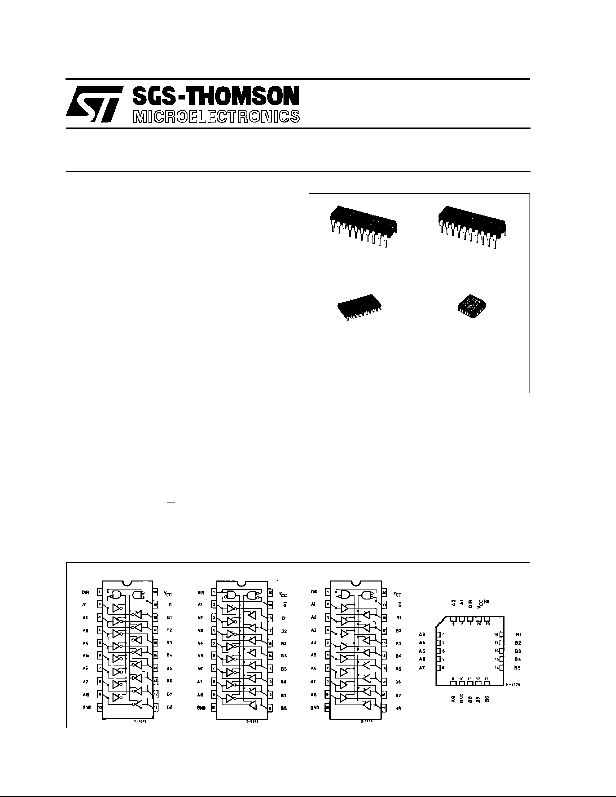
B1R
(PlasticPackage)
F1R
(CeramicPackage)
.SYMMETRICAL OUTPUT IMPEDANCE
|IOH|=IOL=6 mA (MIN)
.BALANCEDPROPAGATIONDELAYS
t
PLH=tPHL
.WIDE OPERATINGRANGE
VCC(OPR)= 2V to 6V
.PIN ANDFUNCTION COMPATIBLE
WITH 54/74LS245/640/643
DESCRIPTION
TheM54/74HC7245 HC7640,HC7643 andHC7645
utilise silicon gate C2MOS technology to achive
operating speeds equivalent to LSTTL devices.
Along withthe low power dissipationand high noise
immunity of standads C2MOS integrated circuit, it
possesses the capability to drive 15 LSTTL loads.
TheseIC’s are intended for two-way asynchronous
communication between data buses, and the
direction of data trasmission is determined by DIR
input.Theenableinput(G)canbeusedtodisablethe
device sothat the buses are effectivelyisolated.
The HC7245/640/7643/7645 have the same pin
configuration and function as the HC245/640/643
andtheyhave a hysteresischaracteristicswith each
input, so HC7245/7640/7643/7645 can be usedas a
line receiver, etc. All input are equipped with
protection circuits against static discharge and
transient excess voltage.
ITISPROHIBITEDTOAPPLYA SIGNALTOA BUS
TERMINAL WHEN IT IS IN OUTPUT MODE AND
WHEN A BUS THERMINAL IS FLOATING (HIGH
IMPEDANCE STATE), IT IS REQUESTED TO FIX
THE INPUT LEVEL BY MEANS OF EXTERNAL
PULLDOWNORPULL UPRESISTOR.
M1R
(MicroPackage)
ORDER CODES :
M54HC XXXXF 1 R M74H CX XXXM1 R
M74HC XXXXB1R M74HCXXXXC1 R
C1R
(Chip Carrier)
PIN CONNECTION (top view)
HC7 640 HC7 643 HC7645/HC7245
HC7245 iselectricallyand funcutionally the same as theHC7645
January 1994
1/10
Page 2
M54/M74HC7245/7640/7643/7645
INPUT AND OUTPUT EQUIVALENT CIRCUIT PIN DESCRIPTION
PIN No SYMBOL NAME AND FUNCTION
1 DIR Directional Control
2, 3, 4, 5,
6, 7, 8, 9
18, 17, 16,
15, 14, 13,
12, 11
19 G Output Enabel Input
10 GND Ground (0V)
20 V
IEC LOGIC SYMBOLS
HC7640 HC764 3 HC7645
A1 to A8 Data Inputs/Outputs
B1 to B8 Data Inputs/Outputs
CC
(Active LOW)
Positive Supply Voltage
TRUTH TABLE
INPUT FUNCTION OUTPUT
G DIR A BUS B BUS HC7640 HC7643 HC7645/7245
L L OUTPUT INPUT A = B A = B A = B
L H INPUT OUTPUT B = A B = A B = A
HXZZZZZ
X: ”H” or ”L”
Z: Highimpedance
2/10
Page 3
M54/M74HC7245/7640/7643/7645
ABSOLU TE M AXI MUM R AT I NG S
Symbol Parameter Value Unit
V
CC
V
V
O
I
IK
I
OK
I
O
I
or I
CC
P
D
T
stg
T
AbsoluteMaximumRatingsarethosevaluesbeyond whichdamagetothedevicemayoccur.Functional operationunder theseconditionisnotimplied.
(*)500 mW:≅ 65oC derate to300 mWby 10mW/oC: 65oCto85oC
RECO MM ENDED OPE RAT IN G CO NDITIO NS
Symbol Parameter Value Unit
V
CC
V
I
V
O
T
op
Supply Voltage -0.5 to +7 V
DC Input Voltage -0.5 to VCC+ 0.5 V
I
DC Output Voltage -0.5 to VCC+ 0.5 V
DC Input Diode Current ± 20 mA
DC Output Diode Current ± 20 mA
DC Output Source Sink Current Per Output Pin ± 35 mA
DC VCCor Ground Current ± 70 mA
GND
Power Dissipation 500 (*) mW
Storage Temperature -65 to +150
Lead Temperature (10 sec) 300
L
Supply Voltage 2 to 6 V
Input Voltage 0 to V
Output Voltage 0 to V
Operating Temperature: M54HC Series
M74HC Series
CC
CC
-55 to +125
-40 to +85
o
C
o
C
V
V
o
C
o
C
3/10
Page 4

M54/M74HC7245/7640/7643/7645
DC SPECIFICATIONS
Test Conditions Value
Symbol Parameter
V
Positive
P
Threshold Voltage
(An, Bn inputs)
N
Negative
V
Threshold Voltage
(An, Bn inputs)
V
H
Hysteresiis
Voltage
(An, Bn inputs)
V
High Level Input
IH
Voltage
(DIR, G inputs)
V
Low Level Input
IL
Voltage
(DIR, G inputs)
OH
High Level
V
Output Voltage
V
Low Level Output
OL
Voltage
Input Leakage
I
I
Current
I
Quiescent Supply
OZ
Current
I
Quiescent Supply
CC
Current
V
CC
(V)
2.0 1 1.25 1.5 1 1.5 1 1.5
4.5 2.3 2.7 3.15 2.3 3.15 2.3 3.15
6.0 3 3.5 4.2 3 4.2 3 4.2
2.0 0.3 0.65 0.9 0.3 0.9 0.3 0.9
4.5 1.13 1.6 2 1.13 2 1.13 2
6.0 1.5 2.3 2.6 1.5 2.6 1.5 2.6
2.0 0.3 0.6 1 0.3 1 0.3 1
4.5 0.6 1.1 1.4 0.6 1.4 0.6 1.4
6.0 0.8 1.2 1.7 0.8 1.7 0.8 1.7
2.0 1.5 1.5 1.5
4.5 3.15 3.15 3.15
6.0 4.2 4.2 4.2
2.0 0.5 0.5 0.5
4.5 1.35 1.35 1.35
6.0 1.8 1.8 1.8
2.0
V
=
I
V
IH
or
V
IL
V
=
I
V
IH
or
V
IL
V
I=VCC
IO=-20 µA
=-6.0 mA 4.18 4.31 4.13 4.10
O
=-7.8 mA 5.68 5.8 5.63 5.60
O
IO=20µA
= 6.0 mA 0.17 0.26 0.33 0.40
O
= 7.8 mA 0.18 0.26 0.33 0.40
O
4.5 4.4 4.5 4.4 4.4
6.0 5.9 6.0 5.9 5.9
4.5 I
6.0 I
2.0
4.5 0.0 0.1 0.1 0.1
6.0 0.0 0.1 0.1 0.1
4.5 I
6.0 I
6.0
6.0 VI=VCCor GND æ0.5 ±5 ±1 µA
6.0 VI=VCCor GND 4 40 80 µA
T
=25oC
A
54HC and 74HC
-40 to 85oC
74HC
-55 to 125oC
54HC
Unit
Min. Typ. Max. Min. Max. Min. Max.
V
V
V
V
V
1.9 2.0 1.9 1.9
V
0.0 0.1 0.1 0.1
V
or GND ±0.1 ±1 ±1 µA
4/10
Page 5

M54/M74HC7245/7640/7643/7645
AC ELECTRICAL CHARACTERISTICS (CL=50pF,Inputtr=tf=6ns)
Test Conditions Value
T
=25oC
Symbol Parameter
t
t
TLH
THL
Output Transition
Time
V
CC
(V)
2.0 25 60 75 90
4.5 7121518
A
54HC and 74HC
Min. Typ. Max. Min. Max. Min. Max.
6.0 6101315
t
PLH
t
PHL
Propagation
Delay Time
2.0 61 125 156 190
4.5 15 25 31 38
6.0 13 21 27 32
t
t
PZL
PZH
Output Enable
Time
2.0
4.5 19 30 38 45
RL=1KΩ
77 150 188 225
6.0 16 26 32 38
t
t
PLZ
PHZ
Output Disable
Time
2.0
4.5 21 30 38 45
RL=1KΩ
84 150 188 225
6.0 18 26 32 38
C
C
Input Capacitance 5 10 10 10 pF
IN
Output
OUT
Capacitance
(*) Power Dissipation
C
PD
Capacitance
(*) CPDisdefined as the valueof the IC’sinternal equivalent capacitance which is calculatedfrom the operating current consumption withoutload.
(RefertoTest Circuit).Average operting current can be obtained bythefollowingequation. ICC(opr) = CPD•VCC•fIN+ICC/4(per Gate)
-40 to 85oC
74HC
-55 to 125oC
54HC
Unit
ns
ns
ns
ns
pF
pF
SWITCHING CHARACTERISTICS TEST WAVEFORM
V
CC
GND
V
CC
GND
5/10
Page 6

M54/M74HC7245/7640/7643/7645
Plastic DIP20 (0.25) MECHANICAL DATA
DIM.
MIN. TYP. MAX. MIN. TYP. MAX.
a1 0.254 0.010
B 1.39 1.65 0.055 0.065
b 0.45 0.018
b1 0.25 0.010
D 25.4 1.000
E 8.5 0.335
e 2.54 0.100
e3 22.86 0.900
F 7.1 0.280
I 3.93 0.155
L 3.3 0.130
Z 1.34 0.053
mm inch
6/10
P001J
Page 7

M54/M74HC7245/7640/7643/7645
Ceramic DIP20 MECHANICAL DATA
DIM.
MIN. TYP. MAX. MIN. TYP. MAX.
A 25 0.984
B 7.8 0.307
D 3.3 0.130
E 0.5 1.78 0.020 0.070
e3 22.86 0.900
F 2.29 2.79 0.090 0.110
G 0.4 0.55 0.016 0.022
I 1.27 1.52 0.050 0.060
L 0.22 0.31 0.009 0.012
M 0.51 1.27 0.020 0.050
N1 4° (min.), 15° (max.)
P 7.9 8.13 0.311 0.320
Q 5.71 0.225
mm inch
P057H
7/10
Page 8

M54/M74HC7245/7640/7643/7645
SO20 MECHANICAL DATA
DIM.
MIN. TYP. MAX. MIN. TYP. MAX.
A 2.65 0.104
a1 0.10 0.20 0.004 0.007
a2 2.45 0.096
b 0.35 0.49 0.013 0.019
b1 0.23 0.32 0.009 0.012
C 0.50 0.020
c1 45° (typ.)
D 12.60 13.00 0.496 0.512
E 10.00 10.65 0.393 0.419
e 1.27 0.050
e3 11.43 0.450
F 7.40 7.60 0.291 0.299
L 0.50 1.27 0.19 0.050
M 0.75 0.029
S8°(max.)
mm inch
8/10
P013L
Page 9

M54/M74HC7245/7640/7643/7645
PLCC20 MECHANICAL DATA
DIM.
MIN. TYP. MAX. MIN. TYP. MAX.
A 9.78 10.03 0.385 0.395
B 8.89 9.04 0.350 0.356
D 4.2 4.57 0.165 0.180
d1 2.54 0.100
d2 0.56 0.022
E 7.37 8.38 0.290 0.330
e 1.27 0.050
e3 5.08 0.200
F 0.38 0.015
G 0.101 0.004
M 1.27 0.050
M1 1.14 0.045
mm inch
P027A
9/10
Page 10

M54/M74HC7245/7640/7643/7645
Information furnished is believed tobe accurateand reliable.However, SGS-THOMSON Microelectronics assumes no responsability for the
consequences of use of such information nor for any infringement of patents or other rights of third partieswhich may results fromits use. No
license isgranted by implication or otherwise underany patent or patent rights ofSGS-THOMSON Microelectronics. Specificationsmentioned
in this publication are subject to changewithout notice. This publication supersedes and replaces all information previously supplied.
SGS-THOMSON Microelectronicsproducts are not authorizedforuse ascritical componentsinlife supportdevices orsystems without express
written approval of SGS-THOMSON Microelectonics.
1994 SGS-THOMSON Microelectronics - All RightsReserved
Australia - Brazil - France - Germany - HongKong - Italy - Japan - Korea - Malaysia - Malta - Morocco - The Netherlands -
Singapore - Spain - Sweden - Switzerland - Taiwan - Thailand - UnitedKingdom - U.S.A
SGS-THOMSON Microelectronics GROUP OF COMPANIES
10/10
 Loading...