

Page 1
M54/74HC696/697
M54/74HC698/699
HC696/698 U/D DEC ADE COUNTER/ REGISTER (3-STATE)
HC697/699 U/D 4 BIT BINARY COU NTER/REG ISTER (3-STATE)
.HIGH SPEED
f
= 50 MHz (TYP.) AT VCC=5V
MAX
.LOWPOWER DISSIPATION
ICC=4µA(MAX.) AT TA=25°C
.HIGH NOISE IMMUNITY
V
NIH=VNIL
.OUTPUT DRIVE CAPABILITY
15 LSTTL LOADS (for QAto QD)
10 LSTTL LOADS (for RCO)
=28%VCC(MIN.)
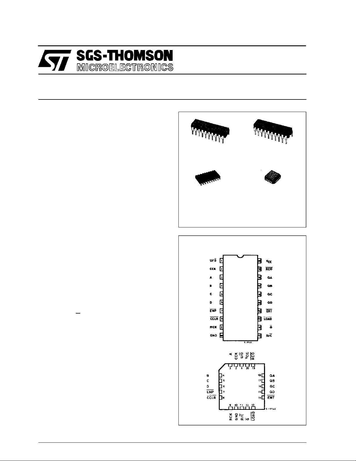
B1R
(PlasticPackage)
F1R
(CeramicPackage)
.SYMMETRICAL OUTPUT IMPEDANCE
|IOH|=IOL=6 mA (MIN.) FOR QATO Q
|IOH|=IOL=4 mA (MIN.) FOR RCO OUTPUT
.BALANCEDPROPAGATIONDELAYS
t
PLH=tPHL
.WIDE OPERATING VOLTAGERANGE
VCC(OPR)= 2 V TO6 V
.PIN AND FUNCTION COMPATIBLE
WITH LSTTL54/74LS696/697/698/699
D
M1R
(MicroPackage)
ORDER CODES :
M54HC X XXF1R M74H CXXXM1R
M74HC X XXB1R M74HCX X XC1R
C1R
(Chip Carrier)
DESCRIPTION
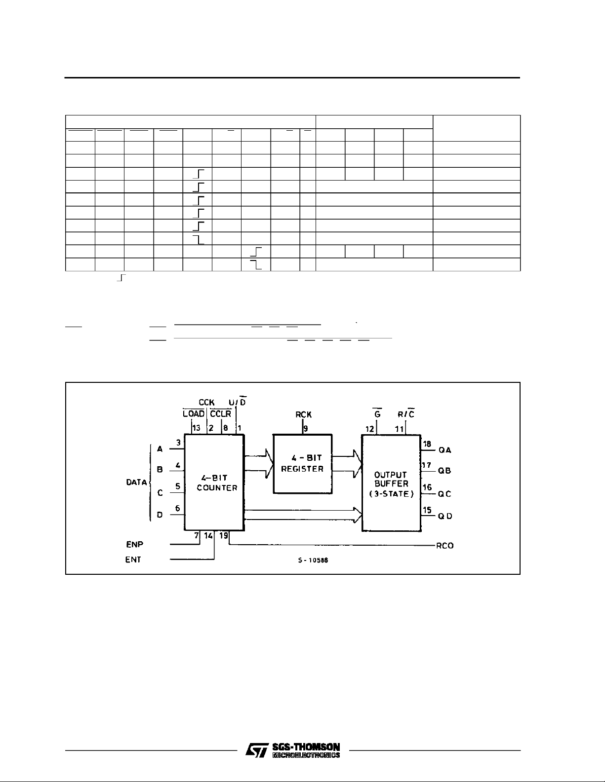
The HC696/697 are high speed CMOS up/down
counters fabricated with silicon gate C2MOS
technology. They achieve the highspeedoperation
similar to equivalent LSTTL while maintaining the
CMOS low power dissipation. The HC696/698 are
BCDDECADECOUNTER, andtheHC697/699 are
4-BIT BINARY COUNTER. Both devices have
register.
Theycount on the positiveedgeofthe counterclock
input(CCK) whenselected by the ”Counter Mode”.
If the input U/D is held ”H”, the internal counter
counts up, and held ”L”, counts down. The internal
counter’s outputs are stored in the output registerat
the positiveedge of registerclock (RCK).
The counter features enable P and enable T and a
ripple-carry output for easy expansion. the
register/counter select input, R/C, selects the
counter when low or the register when high for the
three state outputs, QA, QB, Qc and QD.
Boththe counterclock CCK andregister clock RCK
are positive-edge triggered. The counter clear
CCLR is active low and is synchronous for
HC698/699, and asynchronous for HC696/697.
All inputs are equipped with protection circuits
against static discharge and transient excess
voltage.
PIN CONNECTIONS (top view)
NC =
No Internal
Connection
March1993
1/22
Page 2
M54/M74HC696/697/698/699
PIN DESCRIPTION
PIN No SYMBOL NAME AND FUNCTION
1 U/D Up Down Counter Selector
2 CCK Counter Clock
3, 4, 5, 6 A to D Data Inputs
7, 14 EMP/ENT Enable P and T
8 CCLR Counter Clear (Active
LOW)
9 RCK Register Clock
11 R/C Register Counter Selector
12 G Enable Input
13 LOAD Load Counter (Active
LOW)
15, 16, 17,18QA to QD Data Outputs
19 RCO Load Counter (Active
HIGH)
10 GND Ground (0V)
20 V
CC
Positive Supply Voltage
IEC LOGIC SYMBOL
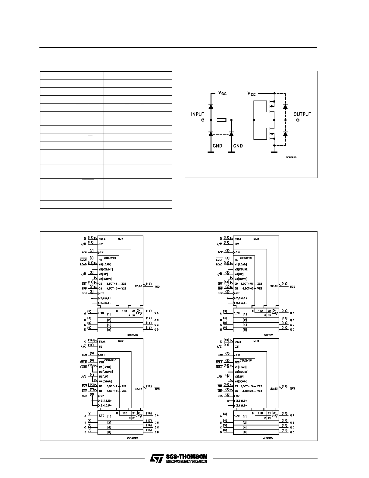
INPUT AND OUTPUT EQUIVALENT CIRCUIT
HC69 6
HC69 8 HC69 9
HC69 7
2/22
Page 3
TRUTH TABLE
M54/M74HC 696/697/698/699
INPUTS OUTPUTS
CCLR LOAD ENP ENT CCK U/D RCK R/C G QA QB QC QD
FUNCTION
XXXXXXXXHZZZZHIGH IMPEDANCE
L X X X X (*) X X L L L L L L CLEAR COUNTER
H L X X X X L L a b c d LOAD COUNTER
H H H X X X L L NO CHANGE NO COUNT
H H X H X X L L NO CHANGE NO COUNT
H H L L H X L L COUNT UP COUNT UP
H H L L L X L L COUNT DOWN COUNT DOWN
H X X X X X L L NO CHANGE NO COUNT
X X X X X X H L a’ b’ c’ d’ LOAD REGISTER
X X X X X X H L NO CHANGE NO LOAD
(*) : ForHC698/699
X : Don’t care
Z : Highimpedance
a-d : The levelof steady stateinputat inputs a throughD respectively
a’-d’ : The levelof steady stateoutputsat internal counter outputsQA’ throughQD’respectively
RCO function : HC696/8 - RCO= (UP• QA • QD • ENT+ UP • QA • QD • ENT)
HC697/9 - RCO = (UP • QA • QB • QC • QD • ENT + UP• QA • QB • QC • QD • ENT)
BLOCK DIAGRAM
3/22
Page 4
M54/M74HC696/697/698/699
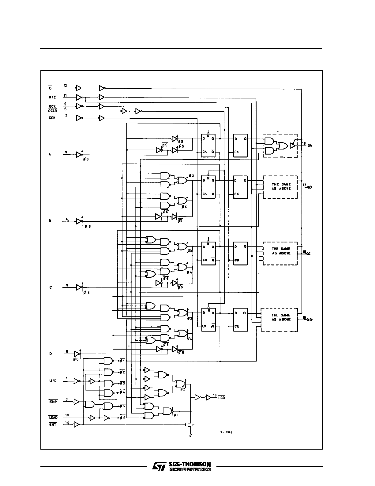
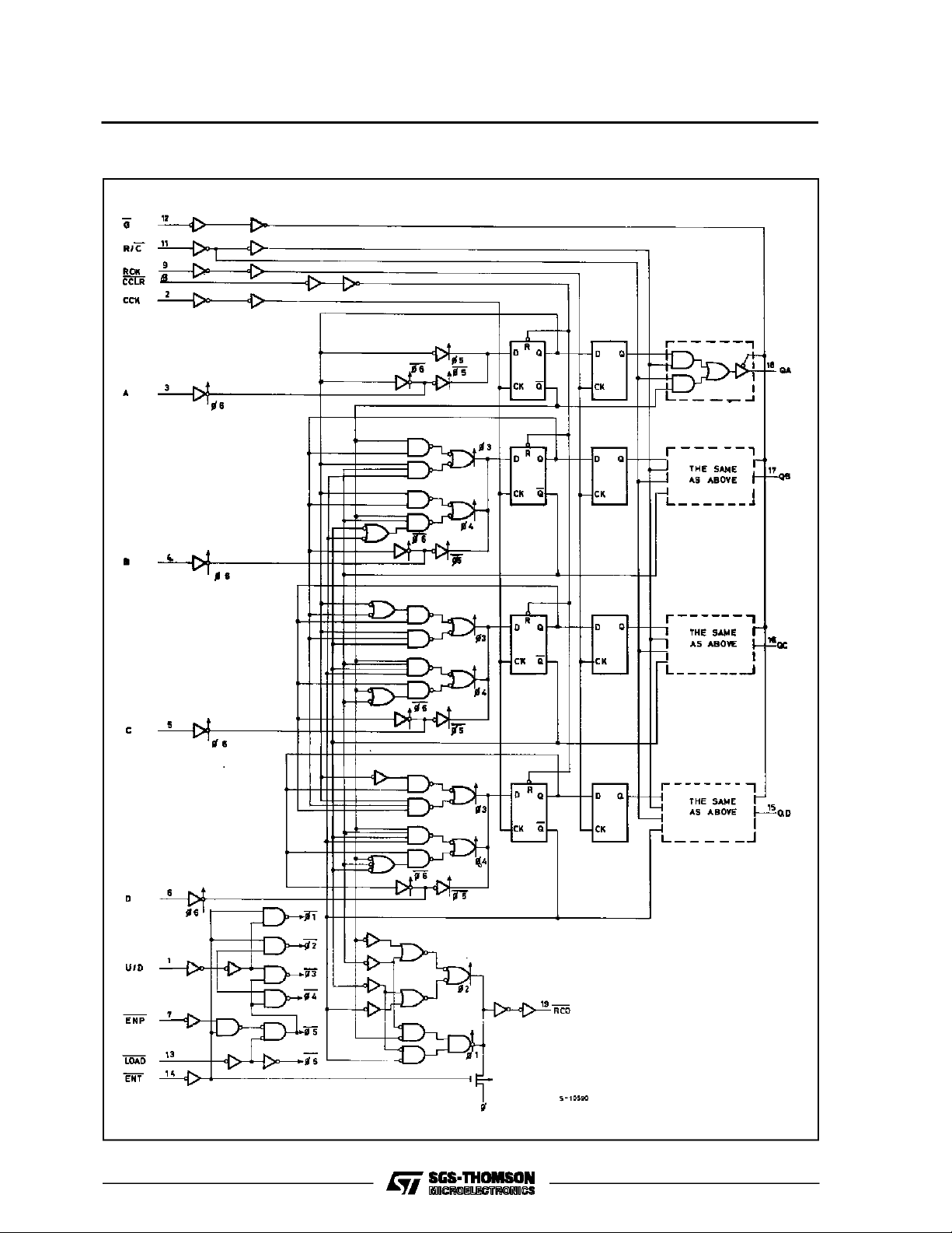
LOGIC DIAGRAM (HC696)
4/22
Page 5
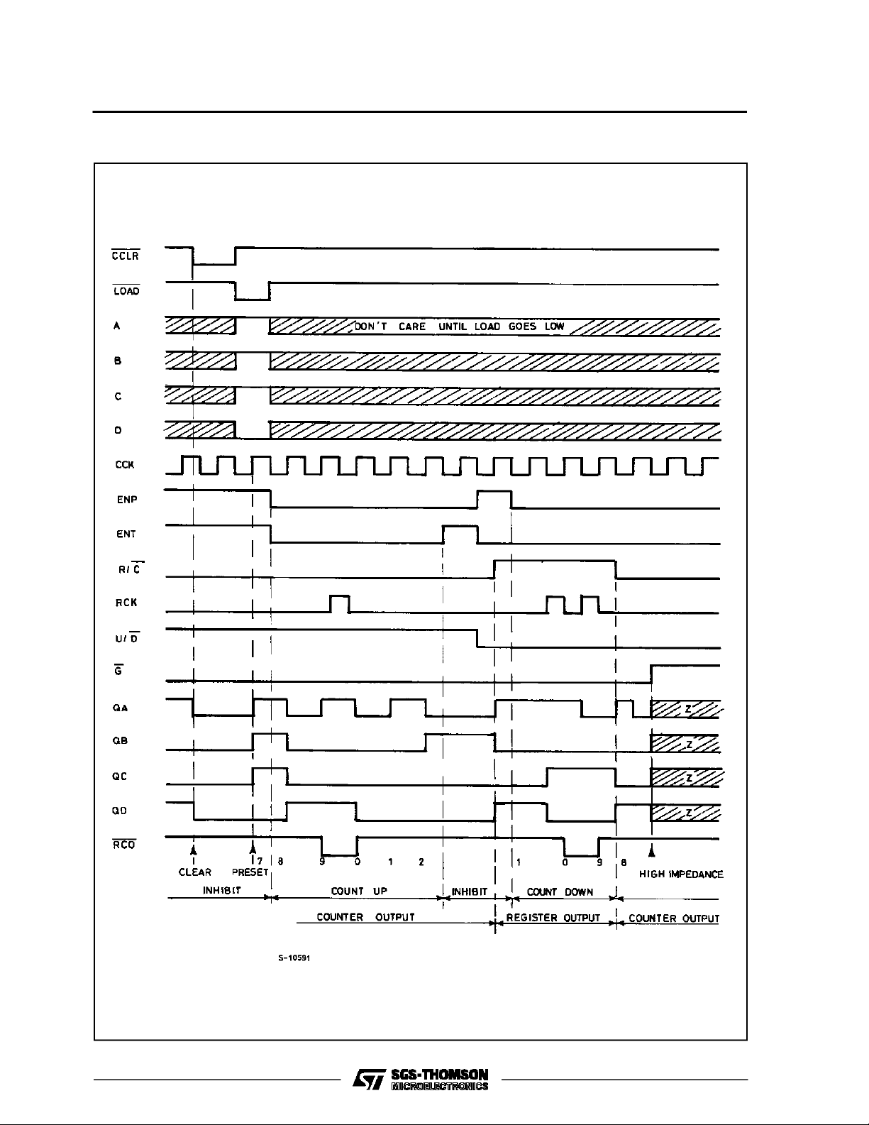
TIMING CHART (HC696)
M54/M74HC 696/697/698/699
5/22
Page 6
M54/M74HC696/697/698/699
LOGIC DIAGRAM (HC697)
6/22
Page 7
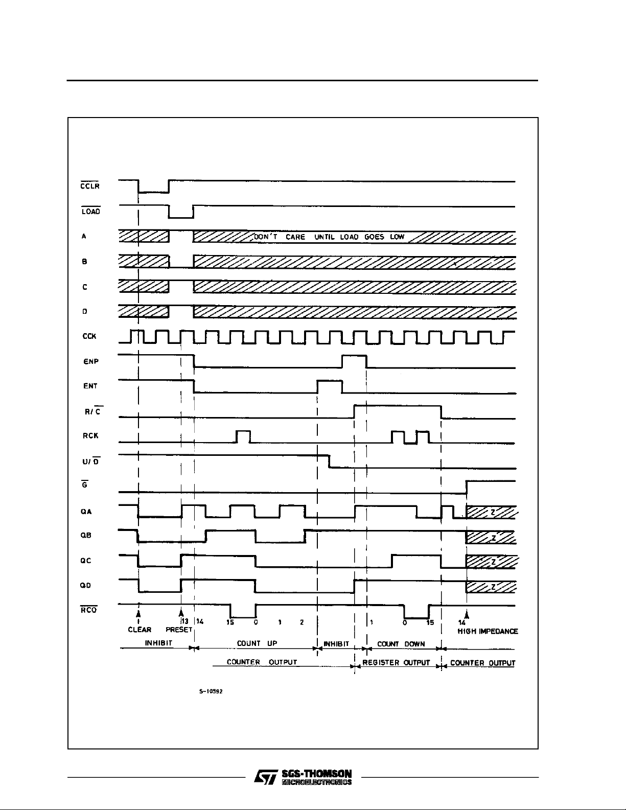
TIMING CHART (HC697)
M54/M74HC 696/697/698/699
7/22
Page 8

M54/M74HC696/697/698/699
LOGIC DIAGRAM (HC698)
8/22
Page 9

DECADE COUNTER, SYNCHRONOUS CLEAR (HC698)
M54/M74HC 696/697/698/699
9/22
Page 10

M54/M74HC696/697/698/699
LOGIC DIAGRAM (HC699)
10/22
Page 11

BINARY COUNTER, SYNCHRONOUS CLEAR (HC699)
M54/M74HC 696/697/698/699
11/22
Page 12

M54/M74HC696/697/698/699
ABSOLU TE MAXIMU M RATI NG S
Symbol Parameter Value Unit
V
CC
V
V
O
I
IK
I
OK
I
O
I
or I
CC
P
D
T
stg
T
AbsoluteMaximumRatings arethose valuesbeyond whichdamage tothedevicemayoccur.Functional operationunder theseconditionisnotimplied.
(*)500 mW:≅ 65oC derate to300 mW by 10mW/oC: 65oCto85oC
RECO MM ENDED O PERAT IN G C ONDITI O NS
Symbol Parameter Value Unit
V
CC
V
I
V
O
T
op
t
r,tf
Supply Voltage -0.5 to +7 V
DC Input Voltage -0.5 to VCC+ 0.5 V
I
DC Output Voltage -0.5 to VCC+ 0.5 V
DC Input Diode Current ± 20 mA
DC Output Diode Current ± 20 mA
DC Output Source Sink Current Per Output Pin (RCO)
(QA to QD)
DC VCCor Ground Current ± 70 mA
GND
± 25
± 35
Power Dissipation 500 (*) mW
Storage Temperature -65 to +150
Lead Temperature (10 sec) 300
L
Supply Voltage 2 to 6 V
Input Voltage 0 to V
Output Voltage 0 to V
Operating Temperature: M54HC Series
M74HC Series
CC
CC
-55 to +125
-40 to +85
Input Rise and Fall Time VCC= 2 V 0 to 1000 ns
V
= 4.5 V 0 to 500
CC
V
= 6 V 0 to 400
CC
mA
o
o
V
V
o
o
C
C
C
C
12/22
Page 13

DC SPECIFICA TIONS
Symbol Parameter
V
V
V
V
V
V
I
I
High Level Input
IH
Voltage
Low Level Input
IL
Voltage
High Level
OH
Output Voltage
(RCO)
High Level
OH
Output Voltage
(QA - QD)
Low Level Output
OL
Voltage
(RCO)
Low Level Output
OL
Voltage
(QA - QD)
I
Input Leakage
I
Current
3 State Output
OZ
Off State Current
Quiescent Supply
CC
Current
M54/M74HC 696/697/698/699
Test Conditions Value
T
=25oC
V
(V)
CC
A
54HC and 74HC
Min. Typ. Max. Min. Max. Min. Max.
2.0 1.5 1.5 1.5
4.5 3.15 3.15 3.15
6.0 4.2 4.2 4.2
2.0 0.5 0.5 0.5
4.5 1.35 1.35 1.35
6.0 1.8 1.8 1.8
2.0
4.5 4.4 4.5 4.4 4.4
6.0 5.9 6.0 5.9 5.9
4.5 I
6.0 I
2.0
4.5 4.4 4.5 4.4 4.4
6.0 5.9 6.0 5.9 5.9
4.5 I
6.0 I
2.0
4.5 0.0 0.1 0.1 0.1
6.0 0.0 0.1 0.1 0.1
4.5 I
6.0 I
2.0
4.5 0.0 0.1 0.1 0.1
6.0 0.0 0.1 0.1 0.1
4.5 I
6.0 I
6.0
6.0
=
V
I
IO=-20 µA
V
IH
or
V
IL
=-4.0 mA 4.18 4.31 4.13 4.10
O
=-5.2 mA 5.68 5.8 5.63 5.60
O
V
=
I
IO=-20 µA
V
IH
or
V
IL
=-6.0 mA 4.18 4.31 4.13 4.10
O
=-7.8 mA 5.68 5.8 5.63 5.60
O
=
V
I
IO=20µA
V
IH
or
V
IL
= 4.0 mA 0.17 0.26 0.33 0.40
O
= 5.2 mA 0.18 0.26 0.33 0.40
O
=
V
I
IO=20µA
V
IH
or
V
IL
= 6.0 mA 0.17 0.26 0.33 0.40
O
= 7.8 mA 0.18 0.26 0.33 0.40
O
VI=VCCor GND ±0.1 ±1 ±1 µA
VI=VIHor V
VO=VCCor GND
1.9 2.0 1.9 1.9
1.9 2.0 1.9 1.9
0.0 0.1 0.1 0.1
0.0 0.1 0.1 0.1
IL
6.0 VI=VCCor GND 4 40 80 µA
-40 to 85oC
74HC
-55 to 125oC
54HC
Unit
±0.5 ±5 ±10 µA
V
V
V
V
V
V
13/22
Page 14

M54/M74HC696/697/698/699
AC ELECTRICAL CHARACTERISTICS (I np ut tr=tf=6ns)
Test Conditions Value
T
=25oC
Symbol Parameter
t
t
TLH
THL
Output Transition
Time
(Qn)
t
TLH
t
THL
Output Transition
Time
(RCO)
t
PLH
t
PHL
Propagation
Delay Time
(CCK - Q)
t
t
PLH
PHL
Propagation
Delay Time
(RCK - Q)
t
t
PLH
PHL
Propagation
Delay Time
(CCK - RCO)
t
t
PLH
PHL
Propagation
Delay Time
(R/C - Q)
t
t
PLH
PHL
Propagation
Delay Time
(ENT - RCO)
t
t
PLH
PHL
Propagation
Delay Time
(CCLR - Q)
t
t
PLH
PHL
Propagation
Delay Time
(CCLR - RCO)
f
MAX
Maximum Clock
Frequency
V
C
CC
(V)
L
(pF)
2.0
50
4.5 7121918
6.0 6101315
2.0
50
4.5 8151923
6.0 7131620
2.0
50
4.5 28 43 54 65
6.0 24 37 46 55
2.0
150
4.5 32 49 61 74
6.0 27 42 52 63
2.0
50
4.5 24 37 46 56
6.0 20 31 39 48
2.0
150
4.5 28 43 54 65
6.0 24 37 46 55
2.0
50
4.5 32 49 61 74
6.0 27 42 52 63
2.0
50
4.5 20 31 39 47
6.0 17 26 33 40
2.0
150
4.5 24 37 46 56
6.0 20 31 39 48
2.0
50
4.5 18 28 35 42
6.0 15 24 30 36
2.0
50
4.5 26 39 49 59
6.0 22 33 42 50
2.0
150
4.5 30 47 59 71
for
HC696
HC697
6.0 26 40 50 60
2.0
50
4.5 29 44 55 66
6.0 25 37 47 56
for
HC696
HC697
2.0
50
4.5 25 45 20 17
6.0 30 53 24 20
A
54HC and 74HC
Min. Typ. Max. Min. Max. Min. Max.
25 60 75 90
30 75 95 115
90 215 270 325
103 245 305 370
82 185 230 280
95 215 270 325
109 245 305 370
61 155 195 235
73 185 230 280
63 140 175 210
78 195 245 295
90 235 295 355
98 220 275 330
5 12 4 3.4
-40 to 85oC
74HC
-55 to 125oC
54HC
Unit
ns
ns
ns
ns
ns
ns
ns
ns
ns
ns
ns
ns
ns
MHz
14/22
Page 15

M54/M74HC 696/697/698/699
AC ELECTRICAL CHARACTERISTICS (Continued)
Test Conditions Value
T
=25oC
Symbol Parameter
t
t
PZL
PZH
Output Enable
Time
C
V
CC
(V)
L
(pF)
2.0
50 RL=1KΩ
4.5 15 24 30 36
A
54HC and 74HC
Min. Typ. Max. Min. Max. Min. Max.
45 120 150 180
6.0 13 20 26 31
2.0
150 R
4.5 19 30 38 45
=1KΩ
L
57 150 190 225
6.0 16 26 32 38
t
t
PLZ
PHZ
Output Disable
Time
2.0
50 RL=1KΩ
4.5 17 23 29 35
32 115 145 175
6.0 14 20 25 30
t
W(H)
t
W(L)
Minimum Pulse
Width
(CCK, RCK)
t
W(L)
Minimum Pulse
Width
(CCLR)
Minimum Set-up
t
s
Time
(CCLR)
Minimum Set-up
t
s
Time (LOAD,
ENT, ENP)
t
Minimum Set-up
s
Time
(A, B, C, D)
Minimum Set-up
t
s
Time
(CCK, RCK)
Minimum Set-up
t
s
Time
(U/D)
Minimum Hold
t
h
Time
2.0
50
4.5 8151922
40 75 95 110
6.0 7131619
2.0
50
4.5 8151922
6.0 7131619
2.0
50
4.5 4101315
6.0 3 9 11 13
2.0
50
4.5 16 30 38 44
for
HC696
HC697
for
HC698
HC699
40 75 95 110
16 50 65 75
64 150 190 220
6.0 14 26 32 37
2.0
50
4.5 4101315
16 50 65 75
6.0 3 9 11 13
2.0
50
4.5 11 20 25 30
44 100 125 150
6.0 9172126
2.0
50
4.5 11 20 25 29
44 100 125 145
6.0 9172125
2.0
50
4.5 5 5 5
6.0 5 5 5
t
REM
Minimum
Removal Time
C
C
PD
Input Capacitance 5 10 10 10 pF
IN
(*) Power Dissipation
Capacitance
(*) CPDisdefined asthe value ofthe IC’s internal equivalent capacitance which is calculated from the operatingcurrent consumption withoutload.
(RefertoTest Circuit).Average operting current can be obtained bythefollowingequation. ICC(opr) = CPD•VCC•fIN+ICC/2(per circuit)
2.0
50
4.5 5 5 5
6.0 5 5 5
HC696/697/699
HC696
HC697
HC698
for
71
77
-40 to 85oC
74HC
-55 to 125oC
54HC
Unit
ns
ns
ns
ns
ns
ns
ns
ns
ns
ns
555
ns
555
ns
pF
15/22
Page 16

M54/M74HC696/697/698/699
SWITCHING CHARACTERISTICS TEST WAVEFORM (HC696/697)
16/22
Page 17

M54/M74HC 696/697/698/699
SWITCHING CHARACTERISTICS TEST WAVEFORM (continued)
OUTPUT DISABLE,ENABLE
TEST CIRCUIT ICC(Opr.)
17/22
Page 18

M54/M74HC696/697/698/699
Plastic DIP20 (0.25) MECHANICAL DATA
DIM.
MIN. TYP. MAX. MIN. TYP. MAX.
a1 0.254 0.010
B 1.39 1.65 0.055 0.065
b 0.45 0.018
b1 0.25 0.010
D 25.4 1.000
E 8.5 0.335
e 2.54 0.100
e3 22.86 0.900
F 7.1 0.280
I 3.93 0.155
L 3.3 0.130
Z 1.34 0.053
mm inch
18/22
P001J
Page 19

M54/M74HC 696/697/698/699
Ceramic DIP20 MECHANICAL DATA
DIM.
MIN. TYP. MAX. MIN. TYP. MAX.
A 25 0.984
B 7.8 0.307
D 3.3 0.130
E 0.5 1.78 0.020 0.070
e3 22.86 0.900
F 2.29 2.79 0.090 0.110
G 0.4 0.55 0.016 0.022
I 1.27 1.52 0.050 0.060
L 0.22 0.31 0.009 0.012
M 0.51 1.27 0.020 0.050
N1 4° (min.), 15° (max.)
P 7.9 8.13 0.311 0.320
Q 5.71 0.225
mm inch
P057H
19/22
Page 20

M54/M74HC696/697/698/699
SO20 MECHANICAL DATA
DIM.
MIN. TYP. MAX. MIN. TYP. MAX.
A 2.65 0.104
a1 0.10 0.20 0.004 0.007
a2 2.45 0.096
b 0.35 0.49 0.013 0.019
b1 0.23 0.32 0.009 0.012
C 0.50 0.020
c1 45° (typ.)
D 12.60 13.00 0.496 0.512
E 10.00 10.65 0.393 0.419
e 1.27 0.050
e3 11.43 0.450
F 7.40 7.60 0.291 0.299
L 0.50 1.27 0.19 0.050
M 0.75 0.029
S8°(max.)
mm inch
20/22
P013L
Page 21

M54/M74HC 696/697/698/699
PLCC20 MECHANICAL DATA
DIM.
MIN. TYP. MAX. MIN. TYP. MAX.
A 9.78 10.03 0.385 0.395
B 8.89 9.04 0.350 0.356
D 4.2 4.57 0.165 0.180
d1 2.54 0.100
d2 0.56 0.022
E 7.37 8.38 0.290 0.330
e 1.27 0.050
e3 5.08 0.200
F 0.38 0.015
G 0.101 0.004
M 1.27 0.050
M1 1.14 0.045
mm inch
P027A
21/22
Page 22

M54/M74HC696/697/698/699
Information furnished is believed to be accurate and reliable. However, SGS-THOMSON Microelectronics assumes no responsability for the
consequences of use of such information nor for any infringement of patents or other rights of third parties which may results from its use. No
license isgranted by implication or otherwise underany patent or patent rights ofSGS-THOMSON Microelectronics. Specificationsmentioned
in this publication are subject to change without notice. This publication supersedes and replaces all information previously supplied.
SGS-THOMSON Microelectronicsproductsare not authorized foruse ascritical componentsinlife supportdevices orsystemswithout express
written approval of SGS-THOMSON Microelectonics.
1994 SGS-THOMSON Microelectronics- All Rights Reserved
Australia - Brazil - France - Germany - Hong Kong - Italy - Japan - Korea - Malaysia - Malta - Morocco - The Netherlands -
Singapore - Spain - Sweden- Switzerland - Taiwan - Thailand - United Kingdom - U.S.A
SGS-THOMSON Microelectronics GROUP OF COMPANIES
22/22
 Loading...