

Page 1
M54/74HC690/691
M54/74HC692/693
HC690/692 DECADE COUNTER/REGISTER (3-STATE)
HC691/693 4 BIT BINARY COUNTER/REGISTER (3-STATE)
.HIGH SPEED
f
= 50 MHz (TYP.) at VCC=5V
MAX
.LOWPOWER DISSIPATION
ICC=4µA(MAX.) at TA=25°C
.HIGH NOISE IMMUNITY
V
NIH=VNIL
.OUTPUT DRIVE CAPABILITY
15 LSTTL LOADS (for QAto QD)
10 LSTTL LOADS (for RCO)
=28%VCC(MIN.)
B1R
(PlasticPackage)
F1R
(CeramicPackage)
.SYMMETRICAL OUTPUT IMPEDANCE
IOH =IOL= 6 mA (MIN.) (for QAtoQD)
IOH =IOL= 4 mA (MIN.) (for RCO)
.BALANCEDPROPAGATIONDELAYS
t
PLH=tPHL
.WIDE OPERATING VOLTAGERANGE
VCC(OPR)= 2 V to 6 V
.PIN AND FUNCTION COMPATIBLE
WITH LSTTL54/74LS690/691
M1R
(MicroPackage)
ORDER CODES :
M54HC X XXF1R M74H CXXXM1R
M74HC X XXB1R M74HCX X XC1R
C1R
(Chip Carrier)
DESCRIPTION
The HC690/691/692/693 are high speed CMOS
COUNTER/REGISTER fabricated in silicon gate
C2MOS technology.
They have the same high speed performance of
LSTTL combined with true CMOS low power consumption.
The internal circuitis composedof 3 stages including buffer output, which offers high noise immunity
andstableoutput.Thesedevices incorporateasynchronous counter, four-bit D-type register, and
quadruple two-line to one-line multiplexers with
three-state outputs in a single 20-pin package. The
counter can be programmed from the data inputs
andhaveenableP andenable Tinputsand a ripplecarry output for easy expansion. The register/counter select input, R/C, selects the counter
when low or the register when high for the threestateoutputs, QA, QB, QC, and QD.
If the LOADinput (LOAD)is held ”L” DATAinput(AD) are loaded in to the internal counter at positive
edge of counter clock input (CCK). In the counter
mode, internal counter counts up at the positive of
the counter clock.If thecounter clear input (CCLR)
isheld”L”, theinternal counteriscleared(synchronously to the counter clock for HC692/HC693, and
asynchronously for HC690/HC691). The internal
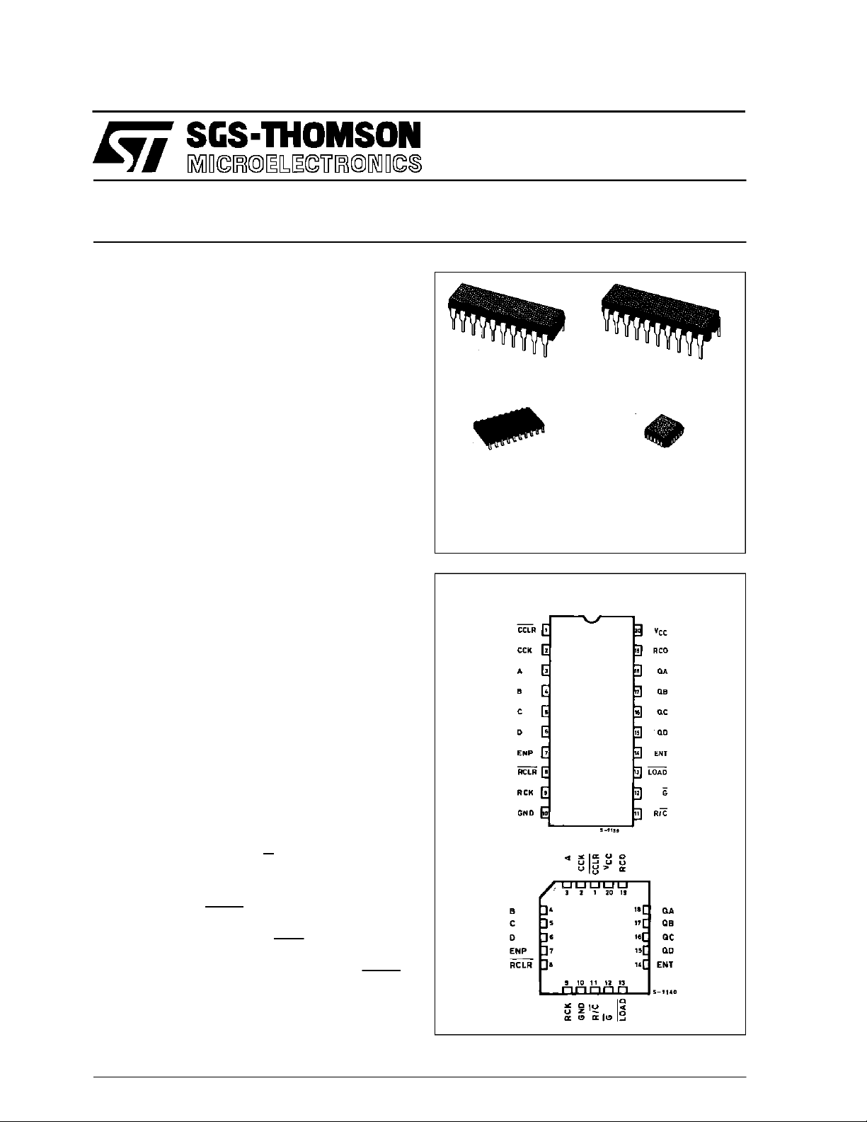
PIN CONNECTIONS (top view)
NC =
No Internal
Connection
March1993
1/23
Page 2
M54/M74HC690/691/692/693
counter’s outputs are stored in the output registerat
the positiveedge of the register clock (RCK). If the
register clear input(RCLR) is held ”L” the registeris
cleared (synchronously to register clock for
HC692/HC693 and asynchronously for
HC690/HC691).Allinputsare equipped withprotection circuits against static discharge and transient
excessvoltage.
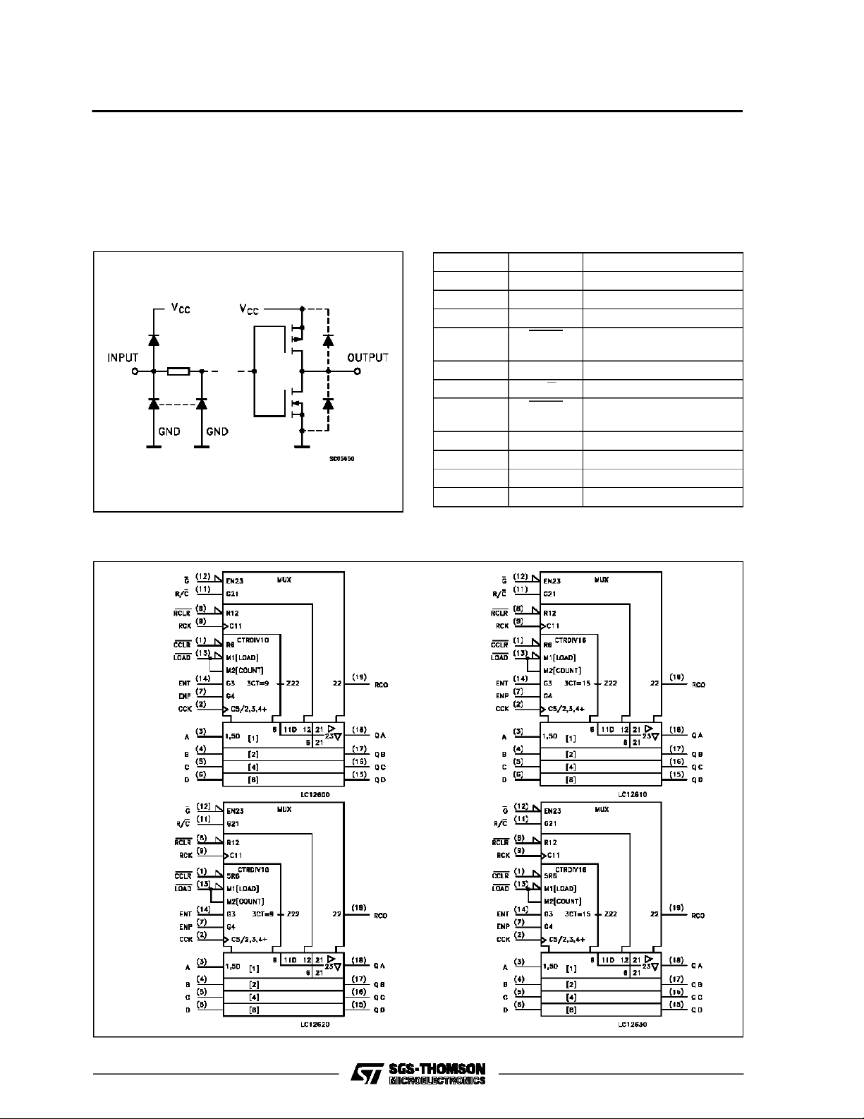
INPUT AND OUTPUT EQUIVALENT CIRCUIT PIN DESCRIPTION
PIN No SYMBOL NAME AND FUNCTION
3 to 6 A to D Data Inputs
7, 14 ENT, ENP Enable Inputs
15 to 18 QA to QD Data Outputs
1 CCLR Counter Clear (Active
2 CCK Counter Clock
11 R/C Counter/ Register Select
8 RCLR Register Clear (Active
9 RCK Register Clock
19 RCO Ripple Counter Output
10 GND Ground (0V)
20 V
CC
IEC LOGIC SYMBOLS
LOW)
LOW)
Positive Supply Voltage
HC69 0
HC69 2 HC69 3
HC69 1
2/23
Page 3
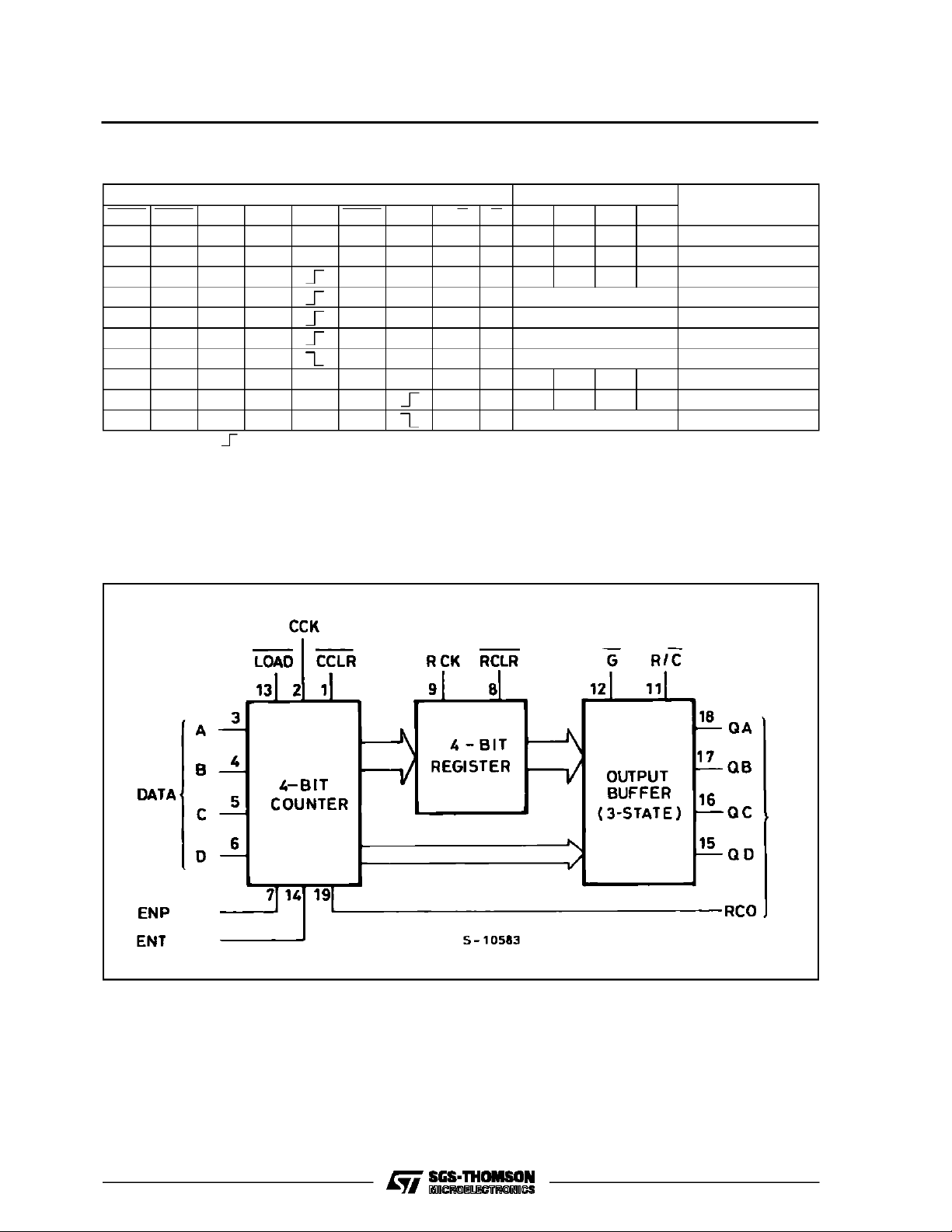
TRUTH TABLE
M54/M74HC 690/691/692/693
INPUTS OUTPUS
CCLR LOAD ENP ENT CCK RCLR RCK R/C G QA QB QC QD
FUNCTION
XXXXXXXXXZZZZHIGH IMPEDANCE
L X X X (*) X X L L L L L L CLEAR COUNTER
H L X X X X L L a b c d LOAD COUNTER
H H L X X X L L NO CHANGE NO COUNT
H H X L X X L L NO CHANGE NO COUNT
H H H H X X L L COUNT UP COUNT UP
H X X X X X L L NO CHANGE NO COUNT
X X X X X L (*) H L L L L L CLEAR REGISTER
X X X X X H H L a’ b’ c’ d’ LOAD REGISTER
X X X X X H H L NO CHANGE NO LOAD
(*): X for HC690/691
X : DON’T CARE
Z : HIGH IMPEDANCE
a-d :THE LEVELOF STEADY STATEINPUTSAT INPUTS ATHROUGHTD RESPECTIVELY.
a’-d’ : THELEVEL OF STEADYSTATE OUTPUTSAT INTERNALCOUNTEROUTPUTSa’ through qd’ respectively
HC690/692 RCO = QA• QD • ENT
HC691/693 RCO = QA• QB • QC • QD • ENT
forHC692/693
BLOCK DIAGRAM
3/23
Page 4
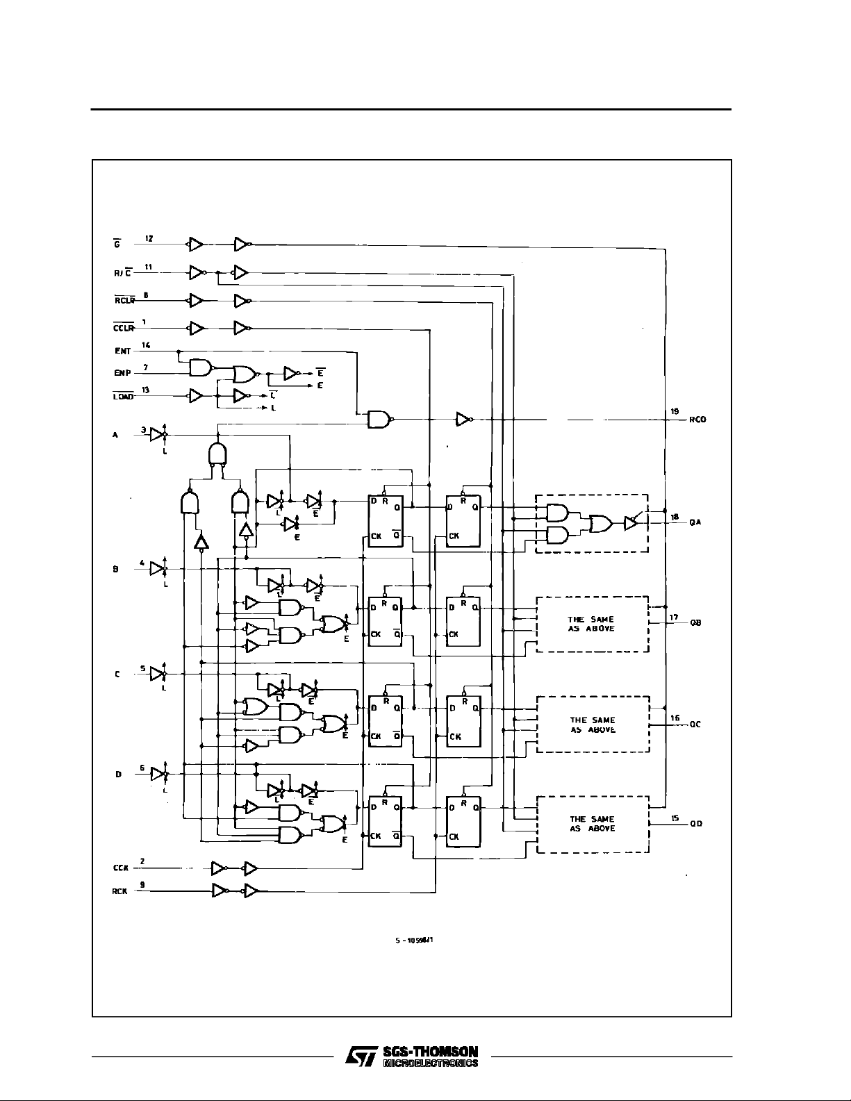
M54/M74HC690/691/692/693
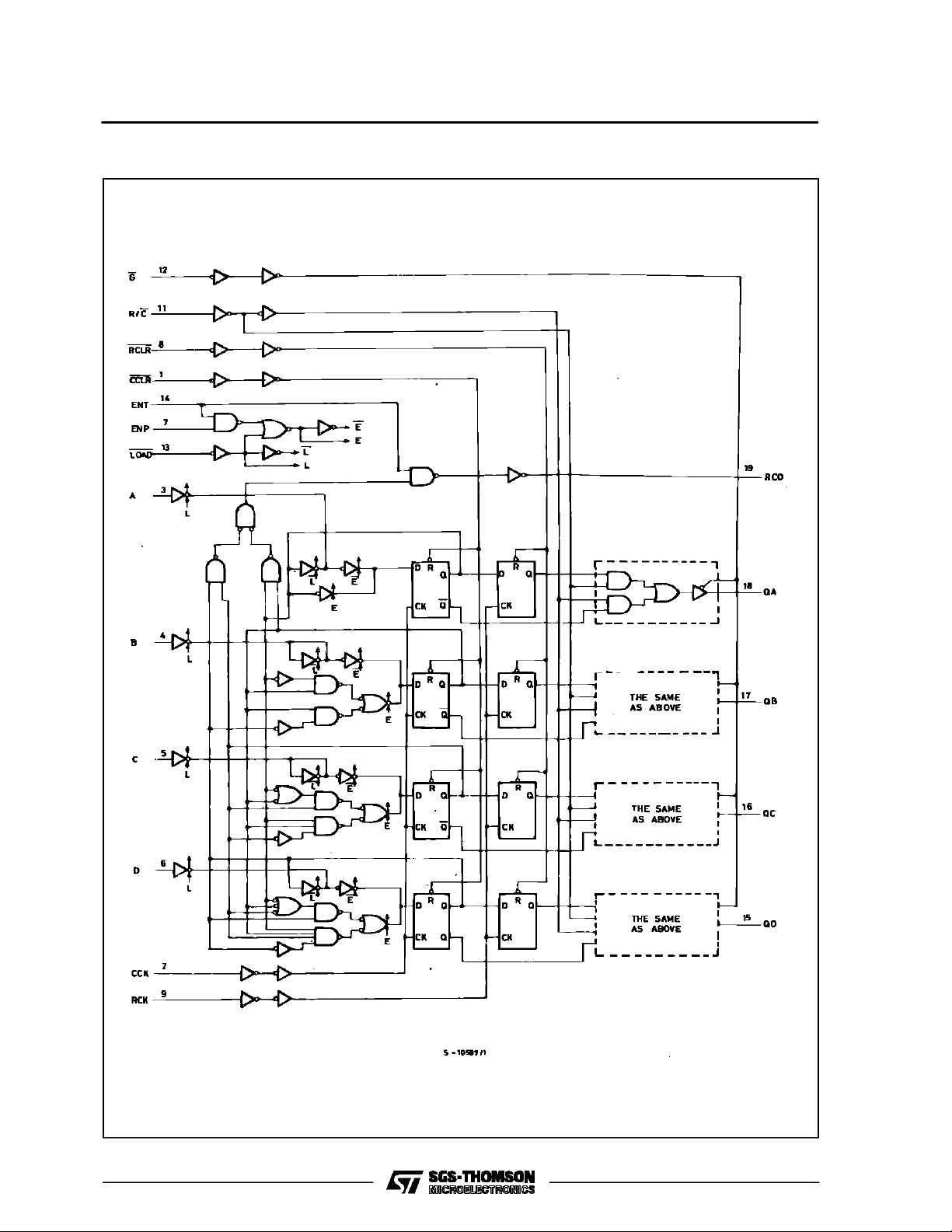
LOGIC DIAGRAM (HC690)
4/23
Page 5
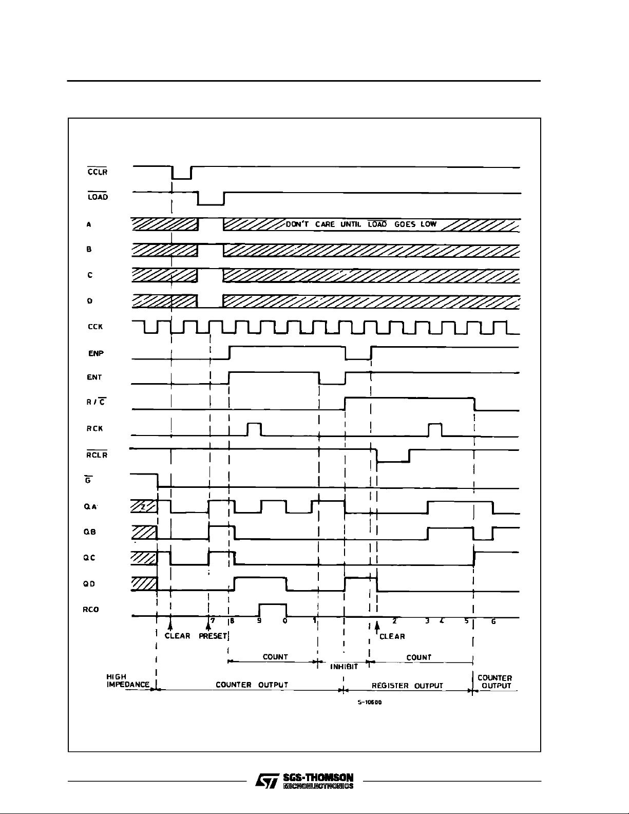
TIMING CHART (HC690)
M54/M74HC 690/691/692/693
5/23
Page 6
M54/M74HC690/691/692/693
LOGIC DIAGRAM (HC691)
6/23
Page 7

TIMING CHART (HC691)
M54/M74HC 690/691/692/693
7/23
Page 8

M54/M74HC690/691/692/693
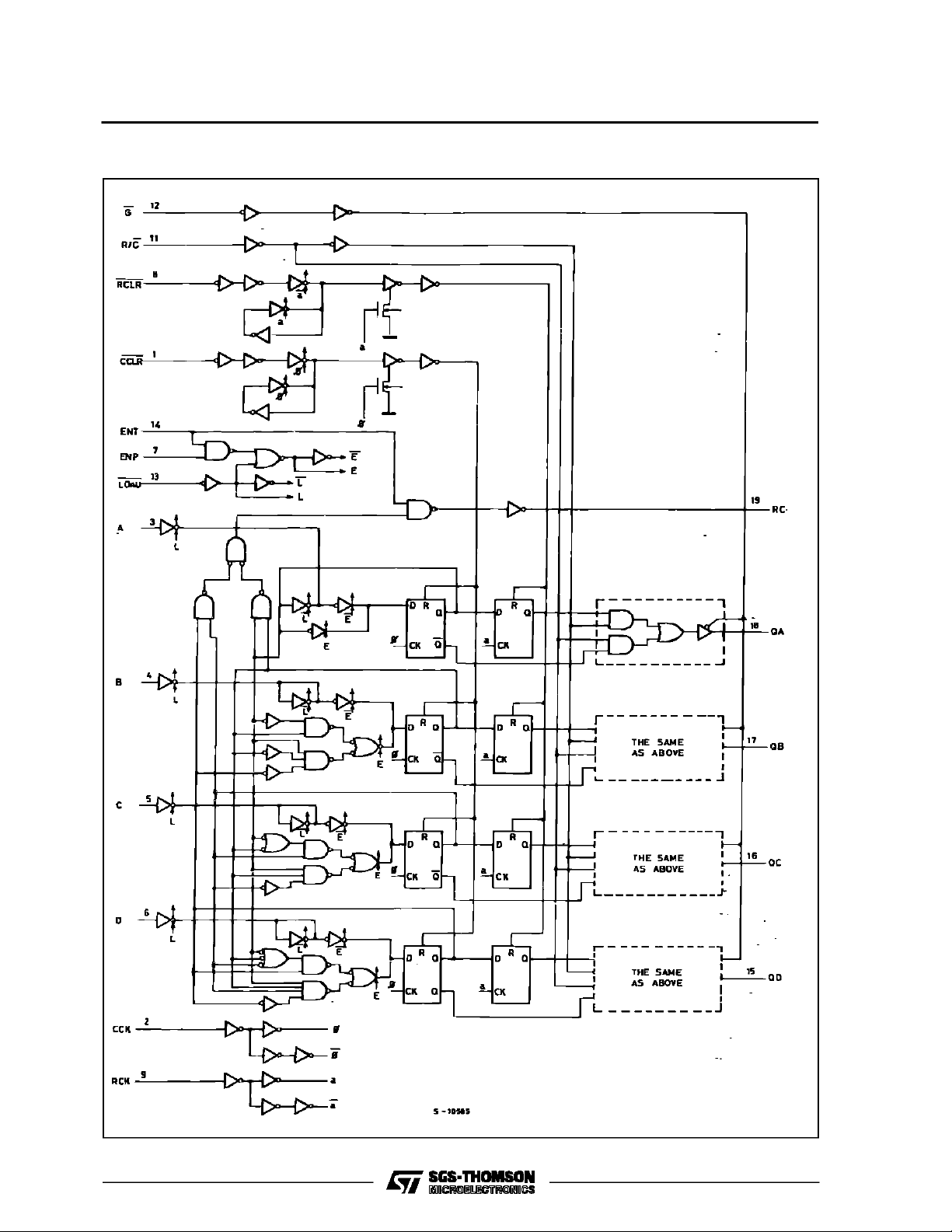
LOGIC DIAGRAM (HC692)
8/23
Page 9

TIMING CHART (HC692)
M54/M74HC 690/691/692/693
9/23
Page 10
M54/M74HC690/691/692/693
LOGIC DIAGRAM (HC693)
10/23
Page 11

TIMING CHART (HC693)
M54/M74HC 690/691/692/693
11/23
Page 12

M54/M74HC690/691/692/693
ABSOLU TE MAXIMUM RATINGS
Symbol Parameter Value Unit
V
CC
V
V
O
I
IK
I
OK
I
O
I
or I
CC
P
D
T
stg
T
AbsoluteMaximumRatings arethose valuesbeyond whichdamage tothedevicemayoccur.Functional operationunder theseconditionisnotimplied.
(*)500 mW:≅ 65oC derate to300 mW by 10mW/oC: 65oCto85oC
RECO MM ENDED OPERAT I N G C O NDITIONS
Symbol Parameter Value Unit
V
CC
V
I
V
O
T
op
t
r,tf
Supply Voltage -0.5 to +7 V
DC Input Voltage -0.5 to VCC+ 0.5 V
I
DC Output Voltage -0.5 to VCC+ 0.5 V
DC Input Diode Current ± 20 mA
DC Output Diode Current ± 20 mA
DC Output Source Sink Current Per
Output Pin
DC VCCor Ground Current ± 70 mA
GND
RCO ± 25 mA
QA to QD ± 35
Power Dissipation 500 (*) mW
Storage Temperature -65 to +150
Lead Temperature (10 sec) 300
L
Supply Voltage 2 to 6 V
Input Voltage 0 to V
Output Voltage 0 to V
Operating Temperature: M54HC Series
M74HC Series
CC
CC
-55 to +125
-40 to +85
Input Rise and Fall Time VCC= 2 V 0 to 1000 ns
V
= 4.5 V 0 to 500
CC
V
= 6 V 0 to 400
CC
o
C
o
C
V
V
o
C
o
C
12/23
Page 13

DC SPECIFICA TIONS
Symbol Parameter
V
V
V
V
V
V
I
I
High Level Input
IH
Voltage
Low Level Input
IL
Voltage
High Level
OH
Output Voltage
(QA - QD)
High Level
OH
Output Voltage
(RCO)
Low Level Output
OL
Voltage
(QA - QD)
Low Level Output
OL
Voltage
(RCO)
I
Input Leakage
I
Current
3 State Output
OZ
Off State Current
Quiescent Supply
CC
Current
M54/M74HC 690/691/692/693
Test Conditions Value
T
=25oC
V
(V)
CC
A
54HC and 74HC
Min. Typ. Max. Min. Max. Min. Max.
2.0 1.5 1.5 1.5
4.5 3.15 3.15 3.15
6.0 4.2 4.2 4.2
2.0 0.5 0.5 0.5
4.5 1.35 1.35 1.35
6.0 1.8 1.8 1.8
2.0
4.5 4.4 4.5 4.4 4.4
6.0 5.9 6.0 5.9 5.9
4.5 I
6.0 I
2.0
4.5 4.4 4.5 4.4 4.4
6.0 5.9 6.0 5.9 5.9
4.5 I
6.0 I
2.0
4.5 0.0 0.1 0.1 0.1
6.0 0.0 0.1 0.1 0.1
4.5 I
6.0 I
2.0
4.5 0.0 0.1 0.1 0.1
6.0 0.0 0.1 0.1 0.1
4.5 I
6.0 I
6.0
=
V
I
IO=-20 µA
V
IH
or
V
IL
=-6.0 mA 4.18 4.31 4.13 4.10
O
=-7.8 mA 5.68 5.8 5.63 5.60
O
V
=
I
IO=-20 µA
V
IH
or
V
IL
=-4.0 mA 4.18 4.31 4.13 4.10
O
=-5.2 mA 5.68 5.8 5.63 5.60
O
=
V
I
IO=20µA
V
IH
or
V
IL
= 6.0 mA 0.17 0.26 0.37 0.40
O
= 7.8 mA 0.18 0.26 0.37 0.40
O
=
V
I
IO=20µA
V
IH
or
V
IL
= 4.0 mA 0.17 0.26 0.37 0.40
O
= 5.2 mA 0.18 0.26 0.37 0.40
O
VI=VCCor GND ±0.1 ±1 ±1 µA
6.0 VI=VIHor V
1.9 2.0 1.9 1.9
1.9 2.0 1.9 1.9
0.0 0.1 0.1 0.1
0.0 0.1 0.1 0.1
IL
VO=VCCor GND
6.0 VI=VCCor GND 4 40 80 µA
-40 to 85oC
74HC
-55 to 125oC
54HC
Unit
±0.5 ±5.0 ±10 µA
V
V
V
V
V
V
13/23
Page 14

M54/M74HC690/691/692/693
AC ELECTRICAL CHARACTERISTICS (CL=50pF,Inputtr=tf=6ns)
Test Conditions Value
Symbol Parameter
t
t
TLH
THL
Output Transition
Time
(Q)
t
TLH
t
THL
Output Transition
Time
(RCO)
t
PLH
t
PHL
Propagation
Delay Time
(CCK - Q)
t
t
PLH
PHL
Propagation
Delay Time
(RCK - Q)
t
t
PLH
PHL
Propagation
Delay Time
(CCK - RCO)
t
t
PLH
PHL
Propagation
Delay Time
(R/C - Q)
t
t
PLH
PHL
Propagation
Delay Time
(ENT - RCO)
t
PHL
Propagation
Delay Time
(CCLR - Q)
(for HC690/691)
t
PHL
Propagation
Delay Time
(RCLR - Q)
(for HC690/691)
t
PHL
Propagation
Delay Time
(CCLR - RCO)
(for HC690/691)
=25oC
T
C
V
CC
(V)
L
(pF)
2.0
50
4.5 7121519
A
54HC and 74HC
Min. Typ. Max. Min. Max. Min. Max.
25 60 75 90
6.0 6101315
2.0
50
4.5 8151923
30 75 95 115
6.0 7131620
2.0
50
4.5 26 41 51 62
82 205 255 310
6.0 22 35 43 53
2.0
150
4.5 30 47 59 71
95 235 295 255
6.0 26 40 50 60
2.0
50
4.5 27 42 53 63
86 210 265 315
6.0 23 36 45 54
2.0
150
4.5 31 48 60 72
99 240 300 360
6.0 26 41 51 61
2.0
50
4.5 21 33 41 50
65 165 205 250
6.0 18 28 35 43
2.0
50
4.5 18 29 36 44
59 145 180 220
6.0 15 25 31 37
2.0
150
4.5 22 35 44 53
72 175 220 265
6.0 19 30 37 45
2.0
50
4.5 12 20 25 30
36 100 125 150
6.0 10 17 21 26
2.0
50
4.5 29 45 56 68
91 225 280 340
6.0 25 38 48 58
2.0
150
4.5 33 51 64 77
104 255 320 385
6.0 28 43 54 65
2.0
50
4.5 27 42 53 63
86 210 265 315
6.0 23 36 45 54
2.0
150
4.5 31 48 60 72
100 240 300 360
6.0 26 41 51 61
2.0
4.5 22 35 44 53
50
70 175 220 265
6.0 19 30 37 45
-40 to 85oC
74HC
-55 to 125oC
54HC
Unit
ns
ns
ns
ns
ns
ns
ns
ns
ns
ns
ns
ns
ns
ns
ns
14/23
Page 15

M54/M74HC 690/691/692/693
AC ELECTRICAL CHARACTERISTICS (Continued)
Test Conditions Value
=25oC
T
Symbol Parameter
f
MAX
Maximum Clock
Frequency
C
V
CC
(V)
L
(pF)
2.0
50
4.5 22 45 18 15
A
54HC and 74HC
Min. Typ. Max. Min. Max. Min. Max.
4.4 12 3.6 3
6.0 26 53 21 18
t
t
PZL
PZH
Output Enable
Time
2.0
50 R
4.5 15 24 30 36
=1KΩ
L
48 120 150 180
6.0 13 20 26 31
2.0
150 R
4.5 19 30 38 45
=1KΩ
L
61 150 190 225
6.0 17 26 32 38
t
t
PLH
PHL
Output Disable
Time
2.0
50 RL=1KΩ
4.5 15 29 36 44
32 145 180 220
6.0 13 25 31 37
t
W(H)
t
W(L)
t
W(L)
Minimum Pulse
Width
(CCK - RCK)
Minimum Pulse
Width
(CCLR - RCLR)
(for HC690/691)
t
Minimum Set-up
s
Time (LOAD,
ENT, ENP)
Minimum Set-up
t
s
Time
(A, B, C, D)
t
Minimum Set-up
s
Time
(CCLR, RCLR)
(for HC692/693)
Minimum Set-up
t
s
Time
(CCK, RCK)
Minimum Hold
t
h
Time
2.0
50
4.5 7151922
28 75 95 110
6.0 6131619
2.0
4.5 8151922
50
40 75 95 110
6.0 7131619
2.0
50
4.5 17 30 38 44
68 150 190 220
6.0 14 26 32 37
2.0
50
4.5 11 20 25 29
44 100 125 145
6.0 9172125
2.0
4.5 11 20 25 29
50
44 100 125 145
6.0 9172125
2.0
50
4.5 12 25 31 36
48 125 155 180
6.0 10 21 26 31
2.0
50
4.5 0 0 0
6.0 0 0 0
t
REM
Minimum
Removal Time
(for HC690/691)
C
C
PD
Input Capacitance 5 10 10 10 pF
IN
(*) Power Dissipation
Capacitance
(*) CPDisdefined asthe value ofthe IC’s internal equivalent capacitance which is calculated from the operatingcurrent consumption withoutload.
(RefertoTest Circuit).Average operting current can be obtained bythefollowingequation. ICC(opr) = CPD•VCC•fIN+I
2.0
50
4.5 5 6 8
6.0 5 5 7
for HC690/691
for HC692/693
70
80
-40 to 85oC
74HC
-55 to 125oC
54HC
Unit
MHz
ns
ns
ns
ns
ns
ns
ns
ns
ns
000
ns
25 30 40
ns
pF
CC
15/23
Page 16

M54/M74HC690/691/692/693
TEST CIRCUIT ICC(Opr.)
SWITCHING CHARACTERISTICS TEST WAVEFORM
forHC690/691
16/23
Page 17

M54/M74HC 690/691/692/693
SWITCHING CHARACTERISTICS TEST WAVEFORM (Continued)
forHC692/693
forALL TYPES
(FixMaximum Count)
17/23
Page 18

M54/M74HC690/691/692/693
SWITCHING CHARACTERISTICS (continued)
t
PLZ,tPZL
The 1 kΩ load resistors should be connected betweenoutputsandVCClineandthe50pF loadcapacitors should be connected between outputs
and GND line.All inputs except G input should be
connected to VCCline or GND line such that outputs will be in low logic level while G input is held
low.
t
PHZ,tPZH
The 1 kΩ load resistors and the50 pF load capacitorsshould be connected between each output
andGND line.
All inputs except G input should be connected to
VCCor GND line such that output will be in high
logic level while G input is held low.
18/23
Page 19

M54/M74HC 690/691/692/693
Plastic DIP20 (0.25) MECHANICAL DATA
DIM.
MIN. TYP. MAX. MIN. TYP. MAX.
a1 0.254 0.010
B 1.39 1.65 0.055 0.065
b 0.45 0.018
b1 0.25 0.010
D 25.4 1.000
E 8.5 0.335
e 2.54 0.100
e3 22.86 0.900
F 7.1 0.280
I 3.93 0.155
L 3.3 0.130
Z 1.34 0.053
mm inch
P001J
19/23
Page 20

M54/M74HC690/691/692/693
Ceramic DIP20 MECHANICAL DATA
DIM.
MIN. TYP. MAX. MIN. TYP. MAX.
A 25 0.984
B 7.8 0.307
D 3.3 0.130
E 0.5 1.78 0.020 0.070
e3 22.86 0.900
F 2.29 2.79 0.090 0.110
G 0.4 0.55 0.016 0.022
I 1.27 1.52 0.050 0.060
L 0.22 0.31 0.009 0.012
M 0.51 1.27 0.020 0.050
N1 4° (min.), 15° (max.)
P 7.9 8.13 0.311 0.320
Q 5.71 0.225
mm inch
20/23
P057H
Page 21

M54/M74HC 690/691/692/693
SO20 MECHANICAL DATA
DIM.
MIN. TYP. MAX. MIN. TYP. MAX.
A 2.65 0.104
a1 0.10 0.20 0.004 0.007
a2 2.45 0.096
b 0.35 0.49 0.013 0.019
b1 0.23 0.32 0.009 0.012
C 0.50 0.020
c1 45° (typ.)
D 12.60 13.00 0.496 0.512
E 10.00 10.65 0.393 0.419
e 1.27 0.050
e3 11.43 0.450
F 7.40 7.60 0.291 0.299
L 0.50 1.27 0.19 0.050
M 0.75 0.029
S8°(max.)
mm inch
P013L
21/23
Page 22

M54/M74HC690/691/692/693
PLCC20 MECHANICAL DATA
DIM.
MIN. TYP. MAX. MIN. TYP. MAX.
A 9.78 10.03 0.385 0.395
B 8.89 9.04 0.350 0.356
D 4.2 4.57 0.165 0.180
d1 2.54 0.100
d2 0.56 0.022
E 7.37 8.38 0.290 0.330
e 1.27 0.050
e3 5.08 0.200
F 0.38 0.015
G 0.101 0.004
M 1.27 0.050
M1 1.14 0.045
mm inch
22/23
P027A
Page 23

M54/M74HC 690/691/692/693
Information furnished is believed to be accurate and reliable. However, SGS-THOMSON Microelectronics assumes no responsability for the
consequences of use of such information nor for any infringement of patents or other rights of third parties which may results from its use. No
license isgranted by implication or otherwise underany patent or patent rights ofSGS-THOMSON Microelectronics. Specificationsmentioned
in this publication are subject to change without notice. This publication supersedes and replaces all information previously supplied.
SGS-THOMSON Microelectronicsproductsare not authorized foruse ascritical componentsinlife supportdevices orsystemswithout express
written approval of SGS-THOMSON Microelectonics.
1994 SGS-THOMSON Microelectronics- All Rights Reserved
Australia - Brazil - France - Germany - Hong Kong - Italy - Japan - Korea - Malaysia - Malta - Morocco - The Netherlands -
Singapore - Spain - Sweden- Switzerland - Taiwan - Thailand - United Kingdom - U.S.A
SGS-THOMSON Microelectronics GROUP OF COMPANIES
23/23
 Loading...