

Page 1
4 WORD X 4 BIT REGISTER FILE (3 STATE)
.HIGH SPEED
tPD= 23 ns(TYP.) AT VCC=5V
.LOWPOWERDISSIPATION
ICC=4µA(MAX.) AT TA=25°C
.HIGH NOISEIMMUNITY
V
NIH=VNIL
=28%VCC(MIN.)
.OUTPUT DRIVE CAPABILITY
10 LSTTL LOADS
.SYMMETRICALOUTPUT IMPEDANCE
|IOH|=IOL=4 mA(MIN.)
.BALANCEDPROPAGATION DELAYS
t
PLH=tPHL
.WIDE OPERATINGVOLTAGE RANGE
VCC(OPR)= 2 V TO6 V
.PIN ANDFUNCTION COMPATIBLE
WITH 54/74LS670
M54HC670
M74HC670
B1R
(PlasticPackage)
M1R
(MicroPackage)
ORDER CODES :
M54HC 670F1R M74H C670M1R
M74HC 670B1R M74HC6 70C1R
F1R
(CeramicPackage)
C1R
(Chip Carrier)
DESCRIPTION
The M54/74HC670 isahighspeedCMOS4 WORD
X 4 BIT REGISTER FILE (3-STATE) fabricated in
silicon gate C2MOS technology. It has the same
high speed performance of LSTTL combined with
true CMOS low power consumption. The
M54HC/74HC670 is a4 x 4 Register File organized
as fourwords by four bits. Separate read andwrite
inputs, both address and enable, allow simultaneousreadand writeoperation. The 3-state outputs
make it possible to connect up to 128outputs to increasethewordcapacity upto512 words.Any number of these devices can be operated in parallel to
generate ann-bitlength.Allinputs areequippedwith
protection circuits against staticdischargeand transient excess voltage.
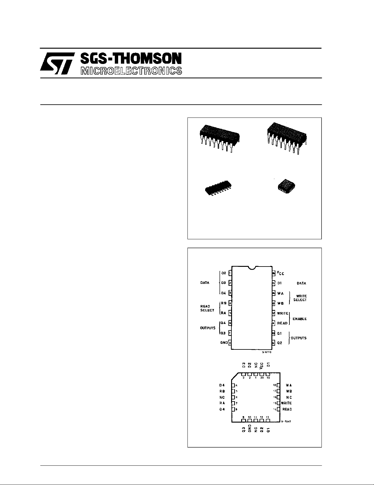
PIN CONNECTIONS(top view)
NC =
No Internal
Connection
October 1992
1/12
Page 2
M54/M74HC670
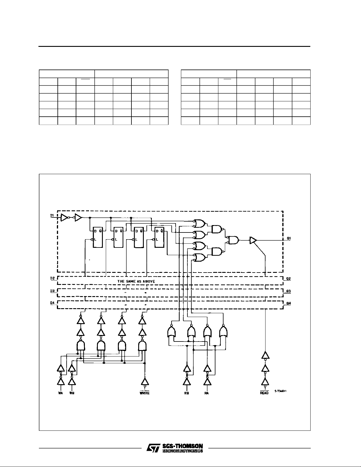
WRIT E FUNCTI ON TAB LE
WRITE INPUTS WORDS
WB WA WE 0 1 2 3
L L LQ=DQ0Q0Q0
LHLQ0Q=DQ0Q0
HLLQ0Q0Q=DQ0
H H L Q0Q0Q0Q=D
X X H Q0 Q0 Q0 Q0
Notes: 1 *: DON’TCARE Z: HIGH IMPEDANCE
2 (Q = D) = THEFOUR SELECT INTERNALFLIP FLOP OUTPUTS WILL ASSUMETHE STATESAPPLIEDTO THE FOUR
EXTERNALDATA INPUTS.
3 Q0 =THE LEVELOF Q BEFORETHE INDICATEDINPUTCONDITIONSWERE ESTABLISHED.
4 W0B1 = THEFIRST BIT OF WORD0, ETC.
READ FUNCTION TABLE
READ INPUTS OUTPUTS
RB RA RE Q0 Q1 Q2 Q3
L L L W0B1 W0B2 W0B3 W0B4
L H L W1B1 W1B2 W1B3 W1B4
H L L W2B1 W2B2 W2B3 W2B4
H H L W3B1 W3B2 W3B3 W3B4
XXHZZZZ
LOGI C DIAG RAM
2/12
Page 3
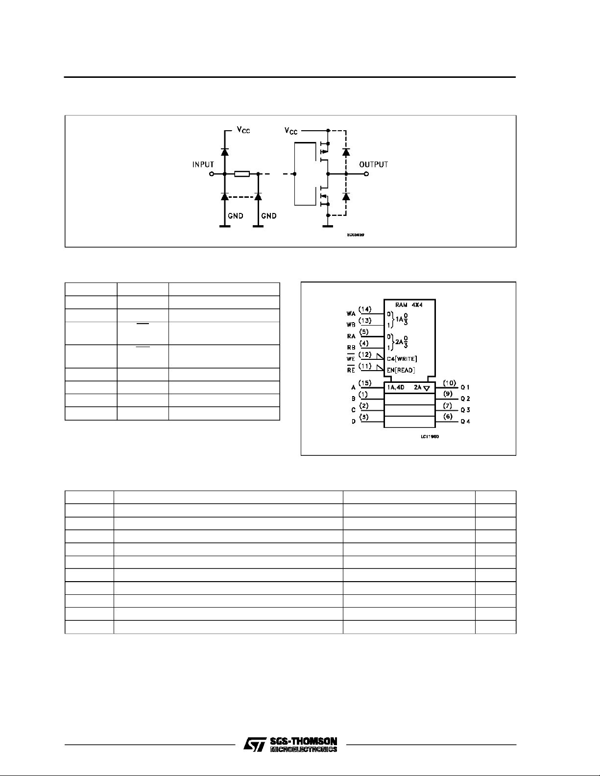
INPUT AND OUTPUT EQUIVALENT CIRCUIT
M54/M74HC670
PIN DESCRIPTION
IEC LOGIC SYMBOL
PIN No SYMBOL NAME AND FUNCTION
5, 4 RA, RB Read Address Inputs
10, 9, 7, 6 Q1 to Q4 Data Outputs
11 RE 3 State Output Read
Enable Input (Active LOW)
12 WE Write Enable Input (Active
LOW)
14, 13 WA, WB Write Address Inputs
15, 1, 2, 3 D1 to D4 Data Inputs
7 GND Ground (0V)
14 V
CC
Positive Supply Voltage
ABSOLU TE M AXI MU M R AT ING S
Symbol Parameter Value Unit
V
CC
V
V
O
I
IK
I
OK
I
O
I
or I
CC
P
D
T
stg
T
AbsoluteMaximumRatingsarethose values beyondwhichdamage tothedevicemayoccur.Functional operation under these conditionisnotimplied.
(*)500 mW: ≅ 65oC derateto300mWby 10mW/oC: 65oCto85oC
Supply Voltage -0.5 to +7 V
DC Input Voltage -0.5 to VCC+ 0.5 V
I
DC Output Voltage -0.5 to VCC+ 0.5 V
DC Input Diode Current ± 20 mA
DC Output Diode Current ± 20 mA
DC Output Source Sink Current Per Output Pin ± 25 mA
DC VCCor Ground Current ± 50 mA
GND
Power Dissipation 500 (*) mW
Storage Temperature -65 to +150
Lead Temperature (10 sec) 300
L
o
C
o
C
3/12
Page 4
M54/M74HC670
RECO MM ENDED OPERAT I N G CO NDITI ONS
Symbol Parameter Value Unit
V
V
V
T
t
r,tf
DC SPECIFICATIO NS
Symbol Parameter
V
IH
V
V
OH
V
OL
I
I
OZ
I
CC
Supply Voltage 2 to 6 V
CC
Input Voltage 0 to V
I
Output Voltage 0 to V
O
Operating Temperature: M54HC Series
op
M74HC Series
CC
CC
-55 to +125
-40 to +85
Input Rise and Fall Time VCC= 2 V 0 to 1000 ns
V
= 4.5 V 0 to 500
CC
V
= 6 V 0 to 400
CC
Test Conditions Value
V
(V)
CC
=25oC
T
A
54HC and 74HC
-40 to 85oC
74HC
-55 to 125oC
Min. Typ. Max. Min. Max. Min. Max.
High Level Input
Voltage
2.0 1.5 1.5 1.5
4.5 3.15 3.15 3.15
6.0 4.2 4.2 4.2
Low Level Input
IL
Voltage
2.0 0.5 0.5 0.5
4.5 1.35 1.35 1.35
6.0 1.8 1.8 1.8
High Level
Output Voltage
Low Level Output
Voltage
Input Leakage
I
Current
3 State Output
Off State Current
Quiescent Supply
2.0
V
=
I
4.5 4.4 4.5 4.4 4.4
6.0 5.9 6.0 5.9 5.9
4.5 I
6.0 I
2.0
4.5 0.0 0.1 0.1 0.1
6.0 0.0 0.1 0.1 0.1
4.5 I
6.0 I
6.0
6.0
IO=-20 µA
V
IH
or
V
IL
=-4.0 mA 4.18 4.31 4.13 4.10
O
=-5.2 mA 5.68 5.8 5.63 5.60
O
V
=
I
IO=20µA
V
IH
or
V
IL
= 4.0 mA 0.17 0.26 0.33 0.40
O
= 5.2 mA 0.18 0.26 0.33 0.40
O
VI=VCCor GND ±0.1 ±1 ±1 µA
VI=VIHor V
VO=VCCor GND
1.9 2.0 1.9 1.9
0.0 0.1 0.1 0.1
IL
±0.5 ±5 ±5 µA
6.0 VI=VCCor GND 4 40 80 µA
Current
54HC
V
V
o
C
o
C
Unit
V
V
V
V
4/12
Page 5

M54/M74HC670
AC ELECTRICAL CHARACTERISTICS (CL=50pF,Inputtr=tf=6ns)
Test Conditions Value
T
=25oC
Symbol Parameter
t
t
TLH
THL
Output Transition
Time
V
CC
(V)
2.0 30 75 95 110
4.5 8151922
A
54HC and 74HC
Min. Typ. Max. Min. Max. Min. Max.
6.0 7131619
t
PLH
t
PHL
t
PLH
t
PHL
t
PLH
t
PHL
t
PZL
t
PZH
Propagation
Delay Time
(RA, RB - Qn)
Propagation
Delay Time
(WE - Qn)
Propagation
Delay Time
(Dn - Qn)
Output Disable
Time
2.0 96 185 230 280
4.5 24 37 46 56
6.0 20 31 39 48
2.0 108 220 275 330
4.5 27 44 55 66
6.0 23 37 47 56
2.0 104 185 230 280
4.5 26 37 46 56
6.0 22 31 39 48
2.0
R
=1KΩ
4.5 13 22 28 33
L
42 110 140 165
6.0 11 19 24 28
t
t
PHZ
PLZ
Output Disable
Time
2.0
4.5 13 19 24 29
RL=1KΩ
25 95 120 145
6.0 11 16 20 25
t
W(L)
Minimum Pulse
Width
(WE)
Minimum Set-up
t
s
Time (Dn - WE)
(WA, WB - WE)
Minimum Hold
t
h
Time
(Dn - WE)
Minimum Hold
t
h
Time
(WA, WB - WE)
t
latch
Minimum Latch
Time
(WE - RA, RB)
C
C
PD
Input Capacitance 5 10 10 10 pF
IN
(*) Power Dissipation
2.0 16 75 95 110
4.5 4151922
6.0 3131619
2.0 12 50 65 75
4.5 3101315
6.0 3 9 11 13
2.0 0 0 0
4.5 0 0 0
6.0 0 0 0
2.0 5 5 5
4.5 5 5 5
6.0 5 5 5
2.0 5 5 5
4.5 5 5 5
6.0 5 5 5
96
Capacitance
(*) CPDisdefined as the value ofthe IC’sinternal equivalent capacitance whichis calculated fromthe operatingcurrentconsumption without load.
(Referto Test Circuit). Average operting current canbe obtained bythe followingequation. ICC(opr) = CPD•VCC•fIN+I
-40 to 85oC
74HC
-55 to 125oC
54HC
CC
Unit
ns
ns
ns
ns
ns
ns
ns
ns
ns
ns
ns
pF
5/12
Page 6

M54/M74HC670
SWITCHING CHARACTERISTICS TEST WAVEFORM
6/12
Page 7

M54/M74HC670
SWITCHING CHARACTERISTICS TEST WAVEFORM (co ntinued)
GND
V
CC
SUCHA LOGIC LEVEL, SHALLBE APPLIEDTO EACH INPUT THAT THE OUTPUT VOLTAGE STAYS IN THE AP-
POSITE SIDE TO THE SWITCHCONNECTIONLEVEL. WHEN THE OUTPUTIS ENABLED.
TEST CIRCUIT ICC(Opr.)
INPUTWAVEFORM IS THE SAME AS THATIN CASEOF SWITCHINGCHARACTERISTICS TEST.
7/12
Page 8

M54/M74HC670
Plastic DIP16 (0.25) MECHANICAL DATA
DIM.
MIN. TYP. MAX. MIN. TYP. MAX.
a1 0.51 0.020
B 0.77 1.65 0.030 0.065
b 0.5 0.020
b1 0.25 0.010
D 20 0.787
E 8.5 0.335
e 2.54 0.100
e3 17.78 0.700
F 7.1 0.280
I 5.1 0.201
L 3.3 0.130
Z 1.27 0.050
mm inch
8/12
P001C
Page 9

Ceramic DIP16/1 MECHANICAL DATA
M54/M74HC670
DIM.
MIN. TYP. MAX. MIN. TYP. MAX.
A 20 0.787
B 7 0.276
D 3.3 0.130
E 0.38 0.015
e3 17.78 0.700
F 2.29 2.79 0.090 0.110
G 0.4 0.55 0.016 0.022
H 1.17 1.52 0.046 0.060
L 0.22 0.31 0.009 0.012
M 0.51 1.27 0.020 0.050
N 10.3 0.406
P 7.8 8.05 0.307 0.317
Q 5.08 0.200
mm inch
P053D
9/12
Page 10

M54/M74HC670
SO16 (Narrow) MECHANICAL DATA
DIM.
MIN. TYP. MAX. MIN. TYP. MAX.
A 1.75 0.068
a1 0.1 0.2 0.004 0.007
a2 1.65 0.064
b 0.35 0.46 0.013 0.018
b1 0.19 0.25 0.007 0.010
C 0.5 0.019
c1 45° (typ.)
D 9.8 10 0.385 0.393
E 5.8 6.2 0.228 0.244
e 1.27 0.050
e3 8.89 0.350
F 3.8 4.0 0.149 0.157
G 4.6 5.3 0.181 0.208
L 0.5 1.27 0.019 0.050
M 0.62 0.024
S8°(max.)
mm inch
10/12
P013H
Page 11

PLCC20 MECHANICAL DATA
M54/M74HC670
DIM.
MIN. TYP. MAX. MIN. TYP. MAX.
A 9.78 10.03 0.385 0.395
B 8.89 9.04 0.350 0.356
D 4.2 4.57 0.165 0.180
d1 2.54 0.100
d2 0.56 0.022
E 7.37 8.38 0.290 0.330
e 1.27 0.050
e3 5.08 0.200
F 0.38 0.015
G 0.101 0.004
M 1.27 0.050
M1 1.14 0.045
mm inch
P027A
11/12
Page 12

M54/M74HC670
Information furnishedis believed to be accurate and reliable. However, SGS-THOMSON Microelectronicsassumes no responsability for the
consequences of useof suchinformation nor forany infringement of patents or other rights of third parties which may results from its use. No
license is granted byimplication or otherwiseunder any patentorpatent rights ofSGS-THOMSON Microelectronics. Specificationsmentioned
in this publication are subjectto changewithout notice. This publication supersedes andreplaces all information previously supplied.
SGS-THOMSON Microelectronicsproducts are not authorized foruse ascritical componentsinlife supportdevices or systemswithoutexpress
written approval of SGS-THOMSON Microelectonics.
1994SGS-THOMSON Microelectronics- All Rights Reserved
Australia -Brazil - France - Germany - Hong Kong - Italy - Japan - Korea - Malaysia - Malta -Morocco - The Netherlands-
Singapore -Spain - Sweden- Switzerland - Taiwan - Thailand- UnitedKingdom - U.S.A
SGS-THOMSON Microelectronics GROUP OFCOMPANIES
12/12
 Loading...