

Page 1
M74HC651
M74HC652
HC651 OCTAL BUS TRANSCEIVE R/REGISTER (3-STATE, INV.)
HC6 52 OCTAL BUS TRANSCE IVER/REG ISTER (3-STATE)
. HIGH SPEED
f
= 73 MHz (TYP.)AT VCC=5V
MAX
.LOWPOWERDISSIPATION
ICC=4µA(MAX.) AT TA=25°C
.HIGH NOISEIMMUNITY
V
NIH=VNIL
=28%V
CC (
MIN.)
.OUTPUT DRIVE CAPABILITY
15 LSTTL LOADS
.SYMMETRICALOUTPUT IMPEDANCE
IOH =IOL= 6 mA(mIN.)
B1R
(PlasticPackage)
M1R
(MicroPackage)
.BALANCEDPROPAGATION DELAYS
t
PLH=tPHL
.WIDE OPERATINGVOLTAGE RANGE
VCC(OPR)= 2 VTO 6V
M74HC X XXM1R M74HC XXXB1R
ORDER CODES :
.PIN ANDFUNCTION COMPATIBLE
WITH 54/74LS651/652
DESCRIPTION
M74HC651/652 are high speed CMOS OCTAL
BUS TRANSCEIVERS AND REGISTERS (3STATE), fabricated in silicongate C2MOS technology. They have the same high speedperformance
ofLSTTLcombined withtrueCMOS low powerconsumption.These devices consist of bustransceiver
circuits, D-type flip-flops, and control circuitry arrangedfor multiplexed transmission ofdatadirectly
from the input bus or fromthe internal storage registers.EnableGABand GBAare provided tocontrol
the transceiver functions.
SelectAB and Select BA control pins are provided
to select whether real-time or stored data is transfered. A low input level selects real-time data, and
a high selects stored data.
Data onthe Aor B bus, or both,can be storedin the
internal D flip-flops by low-to-high transitions at the
appropriate clock pins (CLOCK AB or CLOCK BA)
regardless oftheselectorenablecontrolpins.When
selectAB andselectBA arein thereal-time transfer
mode,it isalso possible to store datawithout using
the internal D-type flip-flops by simultaneously enablingGABandGBA. Inthisconfiguration eachoutput reinforces its input. Thus, when all other data
sources to the two setsof bus lines are at high impedance,each set of buslines will remain at its last
state.Allinputsare equipped withprotectioncircuits
against static discharge and transient excess voltage.
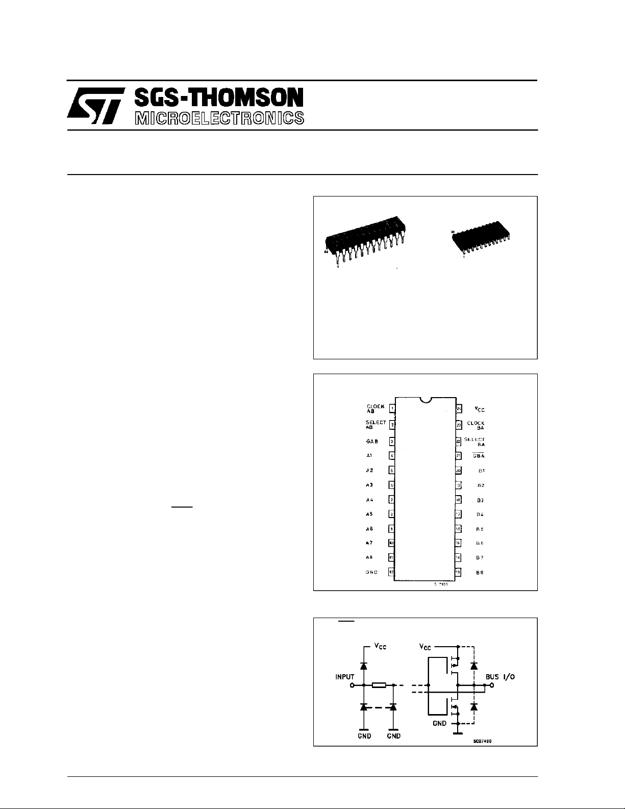
INPUT AND OUTPUT EQUIVALENT CIRCUIT
PIN CONNECTIONS (top view)
GAB,GAB,CAB, A, B
SAB,SBA, CBA
October 1993
1/12
Page 2
M74HC651/652
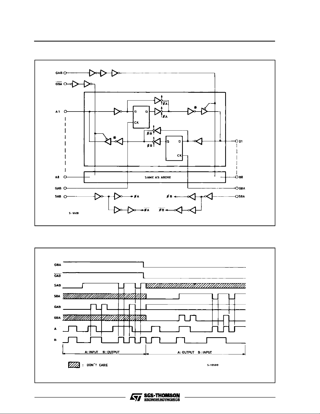
LOGIC DIAGRAM (HC652)
Note: In case ofM74HC652 output invertermarked * atA bus and B busare eliminated.
TIMING CHART
2/12
Page 3
M74HC651/652
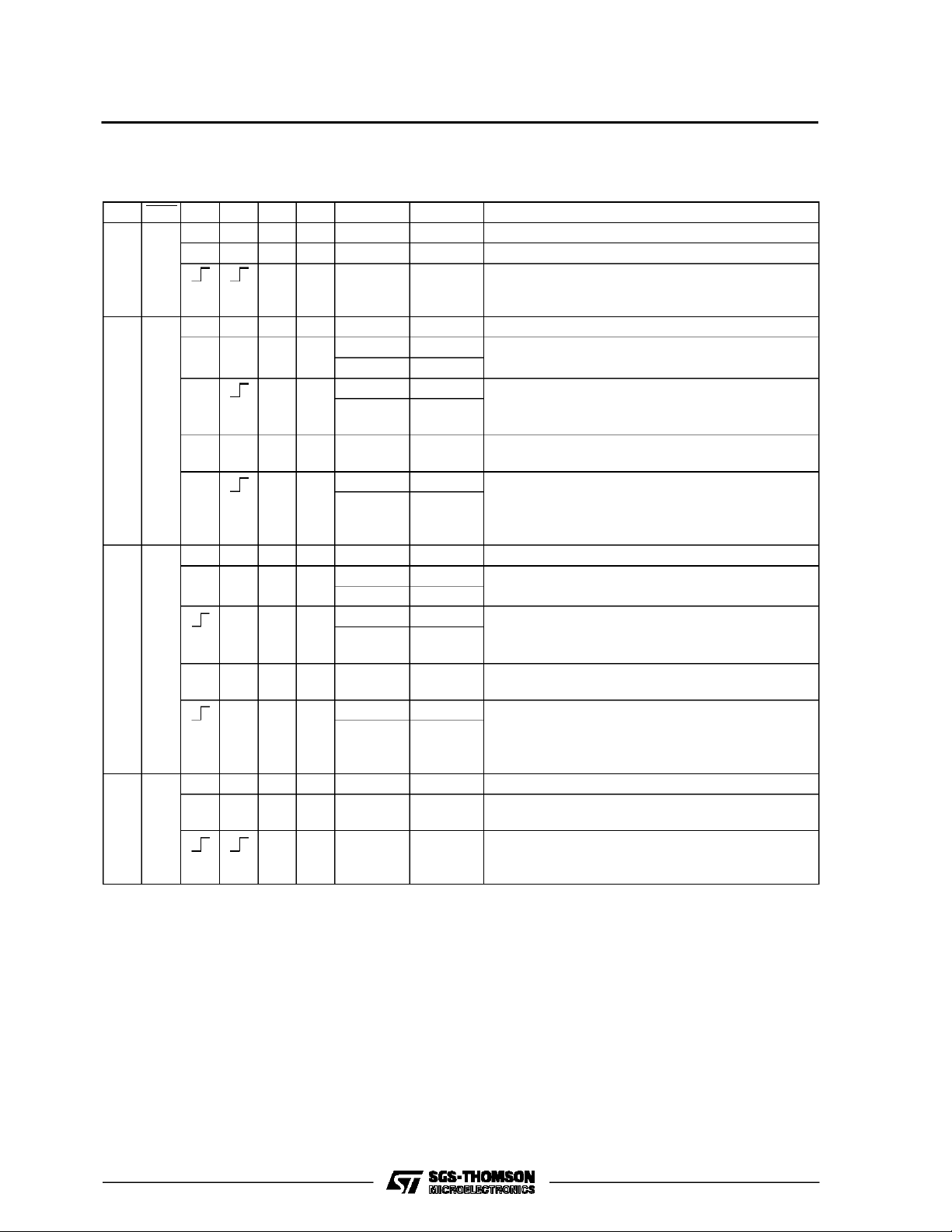
TRUTH TABLE
HC652 ( The truth table for HC651 is t he same as this, but with the outputs inverted)
GAB GBA CAB CBA SAB SBA A B FUNCTION
INPUTS INPUTS Both the A bus and the B bus are inputs
LH
LL
HH
HL
X : DON’TCARE
Z :HIGH IMPEDANCE
Qn :THE DATA STOREDTO THEINTERNALFLIP-FLOPSBY MOST RECENTLOWTO HIGHTRANSITION OF THECLOCK INPUTS
* : THEDATA AT THE A ANDB BUSWILLBE STORED TO THE INTERNALFLIP-FLOPS ON EVERY LOWTO HIGH TRANSITIONOF
THECLOCK INPUTS
X X X X Z Z The output functions of the A and B bus are disabled
X X INPUTS INPUTS Both the A and B buz are used for inputs to the
internal flip-flops. Data at the bus will be stored on
low to high transition of the clock inputs
OUTPUTS INPUTS The A bus are outputs and the B bus are inputs
X* X X L L L The data at the B bus are displayed at the A bus
HH
X* X L L L The data at the B bus ar displayed at the A bus.
HH
The data of the B bus are stored to the internal
flip-flop on low tohigh transition of th clock pulse
X* X X H Qn X The data stored to the internal flip-flop are dispayed
at the A bus
X* X H L L The data at the B bus are stored to the internal flip-
HH
flop on low to high transition of the clock pulse. The
states of the internal flip-flops output directly to the
A bus
INPUTS OUTPUTS The A bus are inputs and the B bus are outputs
XX*L X
L L The data at the A bus are displayed at the B bus
HH
X* L X L L The data at the A bus are displayed at the B bus.
HH
The data of the A bus are stored to the internal flipflop on low to high transition of the clock pulse
X X* H X X Qn The data stored to the internal flip-flops are
displayed at the B bus
X* H X L L the data at the A bus are stored to the internalflip-
HH
flop on low to high transition of the clock pulse. The
states of the internal flip-flops output directly to the
B bus
OUTPUTS OUTPUTS Both the A bus and the B bus are outputs
X X H H Qn Qn The data stored to the internal flip-flops are
displayed at the A and B bus respectively
H H Qn Qn The output at the A bus are displayed at the B bus,
the output at the B bus are displayed at the A bus
respectively
3/12
Page 4
M74HC651/652
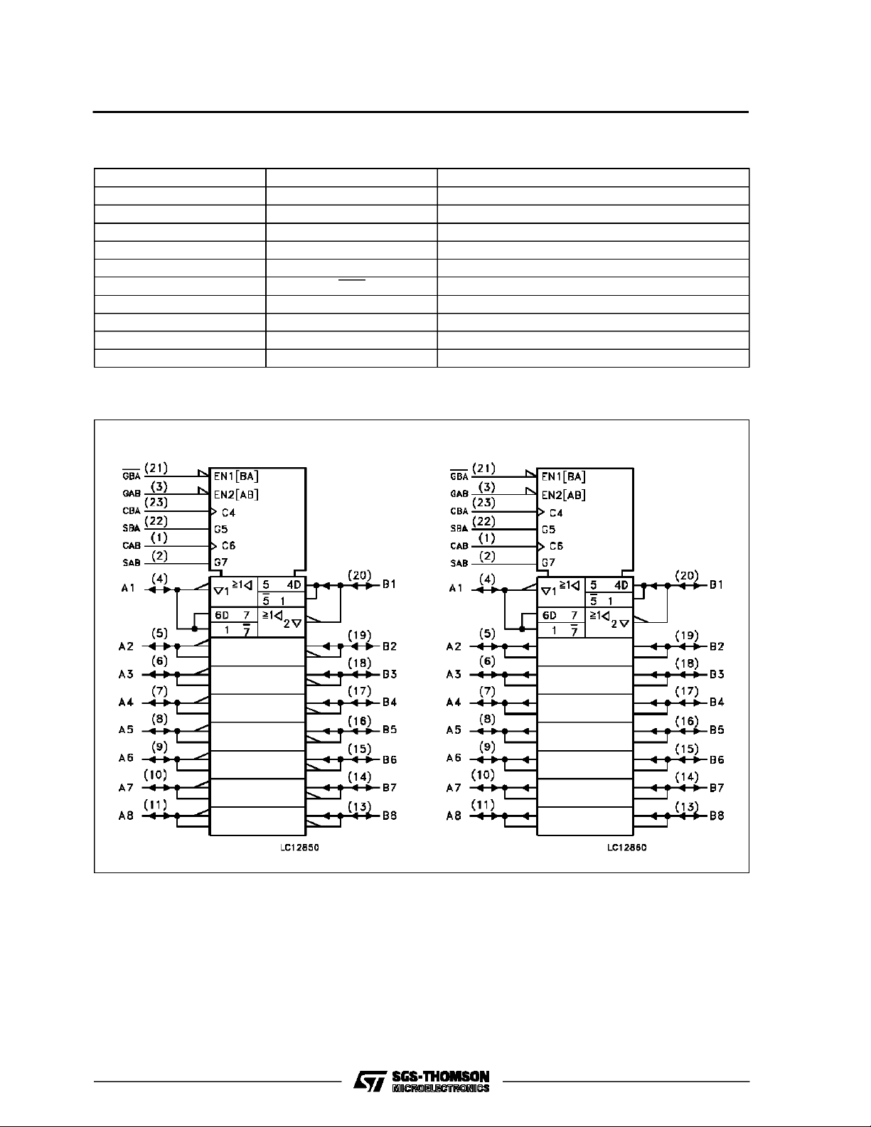
PIN DESCRIPTION
PIN No SYMBOL NAME AND FUNCTION
1 CLOCK AB A to B Clock Input (LOW to HIGH, Edge-Trigged)
2 SELECT AB Select A to B Source Input
3 GAB Direction Control Input
4, 5, 6, 7, 8, 9, 10, 11 A1 to A8 A data Inputs/Outputs
20, 19, 18, 17, 16, 15, 14, 13 B1 to B8 B Data Inputs/Outputs
21 GBA Output Enable Input (Active LOW)
22 SELECT BA Select B to A Source Input
23 CLOCK BA B to A Clock Input (LOW to HIGH, Edge-Triggered)
12 GND Ground (0V)
24 V
IEC LOGIC SYMBOLS
CC
HC651 HC652
Positive Supply Voltage
4/12
Page 5

M74HC651/652
ABSOLU TE M AXI MUM R AT I NG S
Symbol Parameter Value Unit
V
CC
V
V
O
I
IK
I
OK
I
O
I
or I
CC
P
D
T
stg
T
AbsoluteMaximumRatingsarethose values beyondwhichdamage tothedevicemayoccur. Functionaloperationunder these conditionisnotimplied.
(*)500 mW: ≅ 65oC derateto300mWby 10mW/oC: 65oCto85oC
RECO MM ENDED OPERATIN G CO NDI TIONS
Symbol Parameter Value Unit
V
CC
V
I
V
O
T
op
t
r,tf
Supply Voltage -0.5 to +7 V
DC Input Voltage -0.5 to VCC+ 0.5 V
I
DC Output Voltage -0.5 to VCC+ 0.5 V
DC Input Diode Current ± 20 mA
DC Output Diode Current ± 20 mA
DC Output Source Sink Current Per Output Pin ± 35 mA
DC VCCor Ground Current ± 70 mA
GND
Power Dissipation 500 (*) mW
Storage Temperature -65 to +150
Lead Temperature (10 sec) 300
L
Supply Voltage 2 to 6 V
Input Voltage 0 to V
Output Voltage 0 to V
CC
CC
Operating Temperature: -40 to +85
Input Rise and Fall Time VCC= 2 V 0 to 1000 ns
V
= 4.5 V 0 to 500
CC
= 6 V 0 to 400
V
CC
o
C
o
C
V
V
o
C
5/12
Page 6

M74HC651/652
DC SPECIFICATIONS
Symbol Parameter
V
V
V
V
I
I
High Level Input Voltage 2.0 1.5 1.5
IH
Low Level Input
IL
Voltage
High Level Output Voltage 2.0
OH
Low Level Output Voltage 2.0
OL
Input Leakage Current 6.0 VI=VCCor GND ±0.1 ±1 µA
I
I
3 State Output Off State Current 6.0 VI=VIHor V
OZ
Quiescent Supply Current 6.0 VI=VCCor GND 4 40 µA
CC
Test Conditions Value
V
(V)
CC
TA=25oC -40 to 85oC
Min. Typ. Max. Min. Max.
4.5 3.15 3.15
6.0 4.2 4.2
2.0 0.5 0.5
4.5 1.35 1.35
6.0 1.8 1.8
=
V
I
V
IH
or
V
IL
V
I
V
IH
or
V
IL
IO=-20 µA
=-6.0 mA 4.18 4.31 4.13
O
=-7.8 mA 5.68 5.8 5.63
O
=
IO=20µA
= 6.0 mA 0.17 0.26 0.37
O
= 7.8 mA 0.18 0.26 0.37
O
4.5 4.4 4.5 4.4
6.0 5.9 6.0 5.9
4.5 I
6.0 I
4.5 0.0 0.1 0.1
6.0 0.0 0.1 0.1
4.5 I
6.0 I
1.9 2.0 1.9
0.0 0.1 0.1
IL
±0.5 ±5.0 µA
VO=VCCor GND
Unit
V
V
V
V
AC ELECTRICAL CHARACTERISTICS (Inp ut tr=tf=6ns)
Test Conditions Value
Symbol Parameter
t
t
t
t
t
t
TLH
THL
PLH
PHL
PLH
PHL
Output Transition Time 2.0
Propagation Delay Time
(BUS - BUS)
Propagation Delay Time
(CLOCK - BUS)
C
V
CC
(pF)
50
L
Min. Typ. Max. Min. Max.
(V)
4.5 7 12 15
6.0 6 10 13
2.0
50
4.5 21 30 38
6.0 18 26 32
2.0
150
4.5 26 38 48
6.0 22 32 41
2.0
50
4.5 28 42 53
6.0 24 36 45
2.0
150
4.5 33 50 63
6.0 28 43 54
TA=25oC -40 to 85oC
25 60 75
74 150 190
91 190 240
98 210 265
116 250 315
Unit
ns
ns
ns
ns
ns
6/12
Page 7

M74HC651/652
AC ELECTRICAL CHARACTERISTICS (Con t inu ed)
Test Conditions Value
Symbol Parameter
t
t
PLH
PHL
Propagation Delay Time
(SELECT - BUS)
C
V
CC
(V)
L
(pF)
2.0
50
4.5 23 34 43
TA=25oC -40 to 85oC
Min. Typ. Max. Min. Max.
81 170 215
6.0 20 29 37
2.0
150
4.5 28 42 53
98 210 265
6.0 24 36 45
t
t
PZL
PZH
3-State Output Enable Time 2.0
4.5 21 35 44
50 RL=1KΩ
74 175 220
6.0 18 30 37
2.0
150 R
4.5 26 43 54
=1KΩ
L
91 215 270
6.0 22 37 46
t
t
PLZ
PHZ
Output Disable Time 2.0
4.5 21 35 44
50 R
=1KΩ
L
50 175 220
6.0 18 30 37
f
MAX
Maximum Clock Frequency 2.0
4.5 30 67 24
50
6 19 4.8
6.0 35 79 28
t
W(H)
t
W(L)
Minimum Clock Pulse Width 2.0
4.5 7 15 19
50
30 75 95
6.0 6 13 16
Minimum Set-up Time 2.0
t
s
50
4.5 4 10 13
16 50 65
6.0 3 9 11
Minimum Hold Time 2.0
t
h
50
4.5 5 5
55
6.0 5 5
C
C
C
PD
(*) CPDisdefined as the value ofthe IC’sinternal equivalent capacitance whichis calculated fromthe operatingcurrentconsumption withoutload.
(Referto Test Circuit). Average operting current canbe obtained bythefollowingequation. ICC(opr) = CPD•VCC•fIN+ICC/8(per Channel)
Input Capacitance 5 10 10 pF
IN
Bus Terminal Capacitance 10 pF
I/O
(*) Power Dissipation Capacitance for HC651
for HC652
39
38
Unit
ns
ns
ns
ns
ns
MHz
ns
ns
ns
pF
7/12
Page 8

M74HC651/652
SWITCHING CHARACTERISTICS TEST CIRCUIT AND WAVEFORM
WAVEFORM 1 WAVEFORM 2
WAVEFORM3
GBA = ”H”
WAVEFORM5
WAVEFORM 4
GAB= ”L”
8/12
Page 9

TEST WAVEFORM ICC(Opr.)
INPUT TRANSITIONTIME ISTHE SAME ASTHAT INCASE OF SWITCHINGCHARACTERISTICSTEST.
M74HC651/652
9/12
Page 10

M74HC651/652
Plastic DIP24 (0.25) MECHANICAL DATA
DIM.
MIN. TYP. MAX. MIN. TYP. MAX.
a1 0.63 0.025
b 0.45 0.018
b1 0.23 0.31 0.009 0.012
b2 1.27 0.050
D 32.2 1.268
E 15.2 16.68 0.598 0.657
e 2.54 0.100
e3 27.94 1.100
F 14.1 0.555
I 4.445 0.175
L 3.3 0.130
mm inch
10/12
P043A
Page 11

SO24 MECHANICAL DATA
M74HC651/652
DIM.
MIN. TYP. MAX. MIN. TYP. MAX.
A 2.65 0.104
a1 0.10 0.20 0.004 0.007
a2 2.45 0.096
b 0.35 0.49 0.013 0.019
b1 0.23 0.32 0.009 0.012
C 0.50 0.020
c1 45° (typ.)
D 15.20 15.60 0.598 0.614
E 10.00 10.65 0.393 0.420
e 1.27 0.05
e3 13.97 0.55
F 7.40 7.60 0.291 0.299
L 0.50 1.27 0.19 0.050
S8°(max.)
mm inch
L
A
a2
b
e3
D
24 13
112
e
F
s
a1
c1
b1
C
E
11/12
Page 12

M74HC651/652
Information furnishedis believed to be accurate and reliable. However, SGS-THOMSON Microelectronicsassumes no responsability for the
consequences of useof suchinformation nor forany infringement of patents or other rights of third parties which may results from its use. No
license is granted byimplication or otherwiseunder any patentor patentrights ofSGS-THOMSON Microelectronics.Specificationsmentioned
in this publication are subjectto changewithout notice. This publication supersedes andreplaces all information previously supplied.
SGS-THOMSON Microelectronicsproducts are not authorized foruse ascritical componentsinlife supportdevices orsystemswithoutexpress
written approval of SGS-THOMSON Microelectonics.
1994SGS-THOMSON Microelectronics- All Rights Reserved
Australia -Brazil - France - Germany - Hong Kong - Italy - Japan - Korea - Malaysia - Malta -Morocco - The Netherlands-
Singapore -Spain - Sweden- Switzerland - Taiwan - Thailand- UnitedKingdom - U.S.A
SGS-THOMSON Microelectronics GROUP OFCOMPANIES
12/12
 Loading...