

Page 1
M74HC646
M74HC648
HC6 46 OCTA L BUSTRAN S CE I VER / REG I STE R (3-STAT E)
HC648 OCTAL BUS TRANSCEIVER/REGISTER (3-STATE, INV.)
.HIGH SPEED
f
= 73 MHz(TYP.) AT VCC=5V
MAX
.LOWPOWERDISSIPATION
ICC=4µA(MAX.) AT TA=25°C
.HIGH NOISEIMMUNITY
V
NIH=VNIL
.OUTPUT DRIVE CAPABILITY
15 LSTTL LOADS
=28%VCC(MIN.)
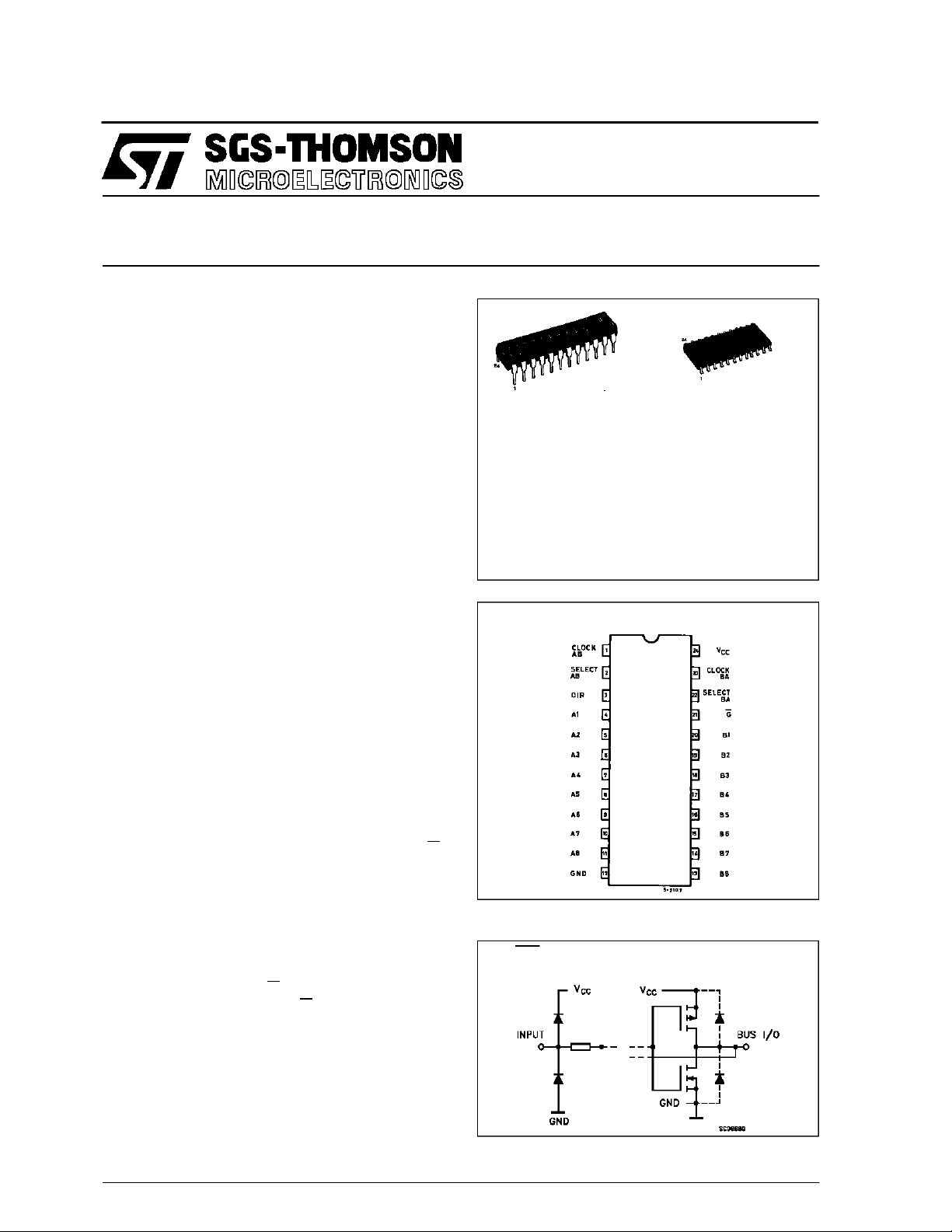
B1R
(PlasticPackage)
M1R
(MicroPackage)
.SYMMETRICALOUTPUT IMPEDANCE
IOH=IOL=6 mA(MIN.)
.BALANCEDPROPAGATION DELAYS
t
PLH=tPHL
.WIDE OPERATINGVOLTAGE RANGE
VCC(OPR)= 2 V TO6 V
M74HC X XXM1R M74H CXXXB1 R
ORDER CODES :
.PIN ANDFUNCTION COMPATIBLE
WITH 54/74LS646/648
DESCRIPTION
The M74HC646/648 are highspeedCMOSOCTAL
BUS TRANSCEIVERS AND REGISTERS, (3STATE) fabricated in silicon gate C2MOS technology. They have the same high speedperformance
ofLSTTLcombined withtrueCMOS low powerconsumption.
These devices consist of bus transceiver circuits
with3-state output, D-typeflip-flops,and controlcircuitryarranged for multiplexed transmission ofdata
directly from the inputbus or from the internal registers.Dataon theAor Bbuswill beclocked intothe
registers on the low-to-high transition of the appropriate clockpin(ClockAB- orClockBA).Enable(G)
and direction (DIR) pins are provided to control the
transceiverfunctions. In thetransceiver mode, data
present at the high-impedance port may be stored
in either register or in both.
The select controls (Select AB select BA) canmultiplex stored and real-time (transparent mode) data.
The direction control determines which bus will receivedata whenenable G is active(low).
In theisolation mode (enable G high),”A” data may
be stored in one register and/or ”B” data may be
storedinthe otherregister.Whenanoutputfunction
is disabled, the input function is still enabled and
may be used to store and transmit data. Only one
of the two buses, A or B, may be driven at a time.
All inputs are equipped with protection circuits
PIN CONNECTIONS (top view)
INPUT AND OUTPUT EQUIVALENT CIRCUIT
GAB,GAB,CAB, A, B
SAB,SBA, CBA
October 1993
1/12
Page 2
M74HC646/648
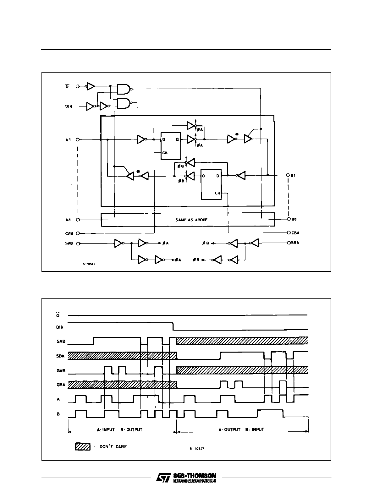
LOGIC DIAGRAM (HC648)
Note: In case ofM54/74HC646 output invertermarked *at A bus and B bus are eliminated.
TIMING CHART
2/12
Page 3
M74HC646/648
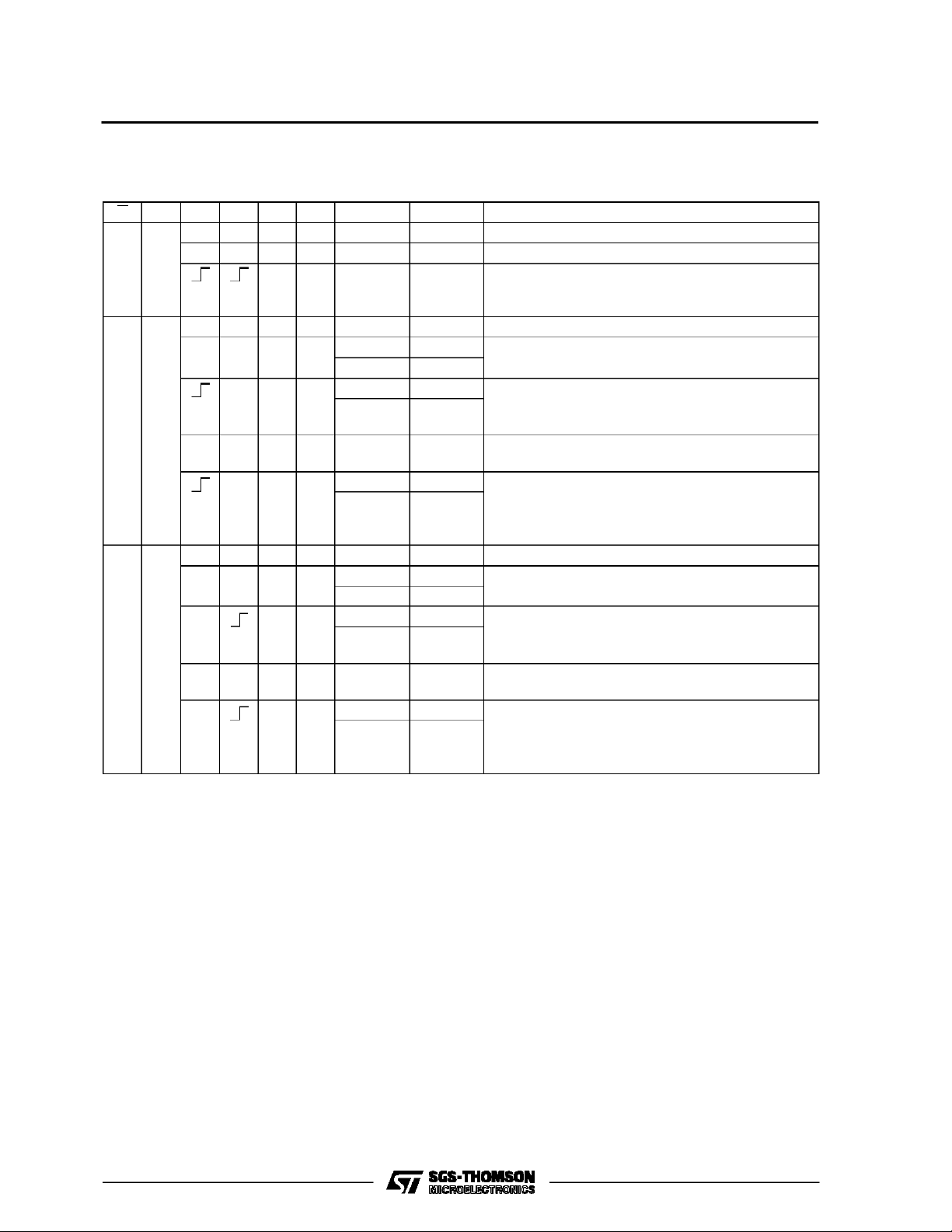
TRUTH TABLE
HC646 ( The truth table for HC648 is the same as this, but with the outputs inverted)
G DIR CAB CBA SAB SBA A B FUNCTION
INPUTS INPUTS Both the A bus and the B bus are inputs
HX
LH
LL
X : DON’TCARE
Z :HIGH IMPEDANCE
Qn :THE DATA STOREDTO THEINTERNALFLIP-FLOPSBY MOST RECENTLOW TO HIGHTRANSITION OF THECLOCK INPUTS
* : THEDATA AT THE A ANDB BUSWILLBE STORED TO THE INTERNALFLIP-FLOPS ON EVERY LOWTO HIGH TRANSITIONOF
THECLOCK INPUTS
X X X X Z Z The output functions of the A and B bus are disabled
X X INPUTS INPUTS Both the A and B bus are used for inputs to the
internal flip-flops. Data at the bus will be stored on
low to high transition of the clock inputs
INPUTS OUTPUTS The A bus are inputs and the B bus are outputs
X X* L X L L The data at the A bus are displayed at the B bus
HH
X* L X L L The data at the A bus are displayed at the B bus.
HH
The data of the A bus are stored to the internal
flip-flop on low to high transition of th clock pulse.
X X* H X X Qn The data stored to the internal flip-flop are dispayed
at the B bus
X* H X L L The data at the A bus are stored to the internal flip-
HH
flop on low to high transition of the clock pulse. The
states of the internal flip-flops output directly to the
B bus
OUTPUTS INPUTS The B bus are inputs and the A bus are outputs
X* X X L
L L The data at the B bus are displayed at the A bus
HH
X* X L L L The data at the B bus are displayed at the A bus.
HH
The data of the B bus are stored to the internal flipflop on low to high transition of the clock pulse
X* X X H Qn X The data stored to the internal flip-flops are
displayed at the A bus
x* X H L L the data at the B bus are stored to the internal flip-
HH
flop on low to high transition of the clock pulse. The
states of the internal flip-flops output directly to the
A bus
3/12
Page 4
M74HC646/648
PIN DESCRIPTION
PIN No SYMBOL NAME AND FUNCTION
1 CLOCK AB A to B Clock Input (LOW to HIGH, Edge-Trigged)
2 SELECT AB Select A to B Source Input
3 GAB Direction Control Input
4, 5, 6, 7, 8, 9, 10, 11 A1 to A8 A data Inputs/Outputs
20, 19, 18, 17, 16, 15, 14, 13 B1 to B8 B Data Inputs/Outputs
21 G Output Enable Input (Active LOW)
22 SELECT BA Select B to A Source Input
23 CLOCK BA B to A Clock Input (LOW to HIGH, Edge-Triggered)
12 GND Ground (0V)
24 V
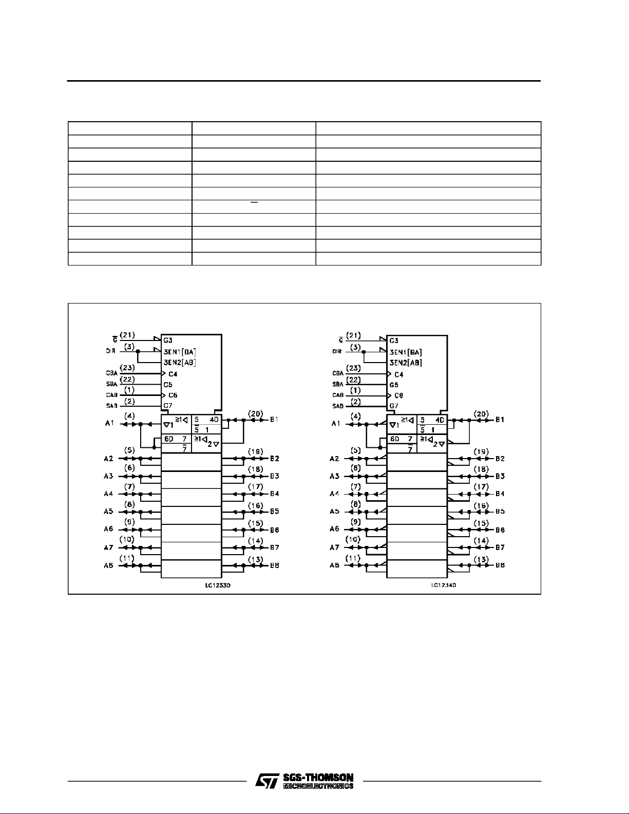
IEC LOGIC SYMBOLS
CC
HC646 HC648
Positive Supply Voltage
4/12
Page 5

M74HC646/648
ABSOLU TE M AXI MUM RATI NG S
Symbol Parameter Value Unit
V
CC
V
V
O
I
IK
I
OK
I
O
I
or I
CC
P
D
T
stg
T
AbsoluteMaximumRatingsarethose valuesbeyond whichdamage tothedevicemayoccur. Functionaloperationunder these condition isnotimplied.
(*)500 mW: ≅ 65oC derateto300 mWby 10mW/oC: 65oCto85oC
RECO MM ENDED OPERAT I N G CO NDI TIONS
Symbol Parameter Value Unit
V
CC
V
I
V
O
T
op
t
r,tf
Supply Voltage -0.5 to +7 V
DC Input Voltage -0.5 to VCC+ 0.5 V
I
DC Output Voltage -0.5 to VCC+ 0.5 V
DC Input Diode Current ± 20 mA
DC Output Diode Current ± 20 mA
DC Output Source Sink Current Per Output Pin ± 35 mA
DC VCCor Ground Current ± 70 mA
GND
Power Dissipation 500 (*) mW
Storage Temperature -65 to +150
Lead Temperature (10 sec) 300
L
Supply Voltage 2 to 6 V
Input Voltage 0 to V
Output Voltage 0 to V
CC
CC
Operating Temperature -40 to +85
Input Rise and Fall Time VCC= 2 V 0 to 1000 ns
V
= 4.5 V 0 to 500
CC
= 6 V 0 to 400
V
CC
o
C
o
C
V
V
o
C
5/12
Page 6

M74HC646/648
DC SPECIFICATIONS
Symbol Parameter
V
V
V
V
I
I
High Level Input Voltage 2.0 1.5 1.5
IH
Low Level Input
IL
Voltage
High Level Output Voltage 2.0
OH
Low Level Output Voltage 2.0
OL
Input Leakage Current 6.0 VI=VCCor GND ±0.1 ±1 µA
I
I
3 State Output Off State Current 6.0 VI=VIHor V
OZ
Quiescent Supply Current 6.0 VI=VCCor GND 4 40 µA
CC
Test Conditions Value
V
(V)
CC
TA=25oC -40 to 85oC
Min. Typ. Max. Min. Max.
4.5 3.15 3.15
6.0 4.2 4.2
2.0 0.5 0.5
4.5 1.35 1.35
6.0 1.8 1.8
=
V
I
V
IH
or
V
IL
V
I
V
IH
or
V
IL
IO=-20 µA
=-6.0 mA 4.18 4.31 4.13
O
=-7.8 mA 5.68 5.8 5.63
O
=
IO=20µA
= 6.0 mA 0.17 0.26 0.37
O
= 7.8 mA 0.18 0.26 0.37
O
4.5 4.4 4.5 4.4
6.0 5.9 6.0 5.9
4.5 I
6.0 I
4.5 0.0 0.1 0.1
6.0 0.0 0.1 0.1
4.5 I
6.0 I
1.9 2.0 1.9
0.0 0.1 0.1
IL
±0.5 ±5.0 µA
VO=VCCor GND
Unit
V
V
V
V
AC ELECTRICAL CHARACTERISTICS (CL=50pF,Inputtr=tf=6ns)
Test Conditions Value
Symbol Parameter
t
t
t
t
t
t
TLH
THL
PLH
PHL
PLH
PHL
Output Transition Time 2.0
Propagation Delay Time
(BUS - BUS)
Propagation Delay Time
(CLOCK - BUS)
V
(V)
CC
C
(pF)
L
TA=25oC -40 to 85oC
Min. Typ. Max. Min. Max.
25 60 75
50
4.5 7 12 15
6.0 6 10 13
2.0
50
4.5 21 30 38
74 150 190
6.0 18 26 32
2.0
150
4.5 26 38 48
91 190 240
6.0 22 32 41
2.0
50
4.5 28 42 53
98 210 265
6.0 24 36 45
2.0
150
4.5 33 50 63
116 250 315
6.0 28 43 54
Unit
ns
ns
ns
ns
ns
6/12
Page 7

M74HC646/648
AC ELECTRICAL CHARACTERISTICS (CL=50pF,Inputtr=tf=6ns)
Test Conditions Value
Symbol Parameter
t
t
PLH
PHL
Propagation Delay Time
(SELECT - BUS)
C
V
CC
(V)
L
(pF)
2.0
50
4.5 23 34 43
TA=25oC -40 to 85oC
Min. Typ. Max. Min. Max.
81 170 215
6.0 20 29 37
2.0
150
4.5 28 42 53
98 210 265
6.0 24 36 45
t
t
PZL
PZH
3-State Output Enable Time
(G, DIR)
2.0
50 RL=1KΩ
4.5 24 35 44
84 175 220
6.0 20 30 37
2.0
150 R
4.5 29 43 54
=1KΩ
L
102 215 270
6.0 25 37 46
t
t
PLZ
PHZ
Output Disable Time
(G, DIR)
2.0
50 R
4.5 23 35 44
=1KΩ
L
60 175 220
6.0 20 30 37
f
MAX
Maximum Clock Frequency 2.0
4.5 30 67 24
50
6 19 4.8
6.0 35 79 28
t
W(H)
t
W(L)
Minimum Clock Pulse Width 2.0
4.5 7 15 19
50
30 75 95
6.0 6 13 16
Minimum Set-up Time 2.0
t
s
50
4.5 4 10 13
16 50 65
6.0 3 9 11
Minimum Hold Time 2.0
t
h
50
4.5 5 5
55
6.0 5 5
C
C
C
PD
(*) CPDisdefined as the value ofthe IC’sinternal equivalent capacitance which is calculated fromthe operatingcurrent consumption without load.
(Referto Test Circuit). Average operting current canbe obtained bythe followingequation. ICC(opr) = CPD•VCC•fIN+ICC/8(per bit)
Input Capacitance 5 10 10 pF
IN
Bus Terminal Capacitance 10 pF
I/O
(*) Power Dissipation Capacitance for HC646
for HC648
39
38
Unit
ns
ns
ns
ns
ns
MHz
ns
ns
ns
pF
7/12
Page 8

M74HC646/648
SWITCHING CHARACTERISTICS TEST CIRCUIT AND WAVEFORM
WAVEFORM 1 WAVEFORM 2
WAVEFORM3
WAVEFORM 4
WAVEFORM5
8/12
Page 9

TEST WAVEFORM ICC(Opr.)
* INPUTTRANSITION TIMEIS THE SAME AS THATIN CASEOF SWITCHINGCHARACTERISTICSTEST.
M74HC646/648
9/12
Page 10

M74HC646/648
Plastic DIP24 (0.25) MECHANICAL DATA
DIM.
MIN. TYP. MAX. MIN. TYP. MAX.
a1 0.63 0.025
b 0.45 0.018
b1 0.23 0.31 0.009 0.012
b2 1.27 0.050
D 32.2 1.268
E 15.2 16.68 0.598 0.657
e 2.54 0.100
e3 27.94 1.100
F 14.1 0.555
I 4.445 0.175
L 3.3 0.130
mm inch
10/12
P043A
Page 11

SO24 MECHANICAL DATA
M74HC646/648
DIM.
MIN. TYP. MAX. MIN. TYP. MAX.
A 2.65 0.104
a1 0.10 0.20 0.004 0.007
a2 2.45 0.096
b 0.35 0.49 0.013 0.019
b1 0.23 0.32 0.009 0.012
C 0.50 0.020
c1 45° (typ.)
D 15.20 15.60 0.598 0.614
E 10.00 10.65 0.393 0.420
e 1.27 0.05
e3 13.97 0.55
F 7.40 7.60 0.291 0.299
L 0.50 1.27 0.19 0.050
S8°(max.)
mm inch
L
A
a2
b
e3
D
24 13
112
e
F
s
a1
c1
b1
C
E
11/12
Page 12

M74HC646/648
Information furnishedis believed to be accurate and reliable. However, SGS-THOMSON Microelectronicsassumes no responsability for the
consequences of useof suchinformation nor for any infringement of patents or other rights of third parties which may results from its use. No
license is granted byimplication or otherwiseunder any patentor patentrights ofSGS-THOMSON Microelectronics.Specificationsmentioned
in this publication are subjectto changewithout notice. This publication supersedes andreplaces all information previouslysupplied.
SGS-THOMSON Microelectronicsproducts are not authorized foruse ascritical componentsinlife supportdevices or systems without express
written approval of SGS-THOMSON Microelectonics.
1994SGS-THOMSON Microelectronics- All Rights Reserved
Australia -Brazil - France - Germany - Hong Kong - Italy - Japan - Korea - Malaysia - Malta -Morocco - The Netherlands-
Singapore -Spain - Sweden- Switzerland - Taiwan - Thailand- UnitedKingdom - U.S.A
SGS-THOMSON Microelectronics GROUP OFCOMPANIES
12/12
 Loading...