

Page 1
M54/74HC245/640/643
M54/74HC245/640/643
October1993
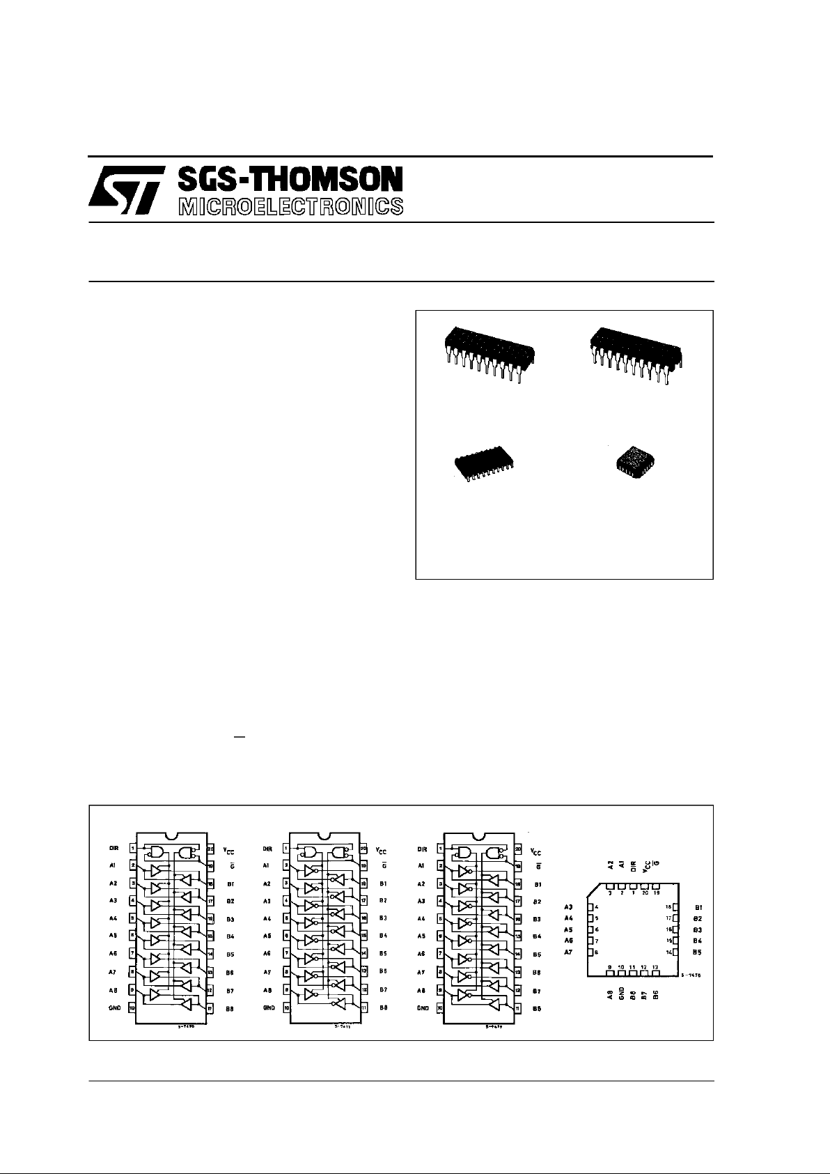
HC640 INVERTING, HC643 INVERTING/NON INVERTING
OCTALBUS TRANSCEIVER(3-STATE):HC24 5 NONINVERTING
B1R
(PlasticPackage)
ORDER CODES :
M54HC X XXF1R M74HC XXXM1R
M74HC X XXB1R M74HCXXXC1 R
F1R
(CeramicPackage)
M1R
(MicroPackage)
C1R
(Chip Carrier)
PIN CONNECTION (top view)
.HIGH SPEED
tPD= 10 ns(TYP.) at VCC=5V
.LOWPOWER DISSIPATION
ICC=4µA (MAX.) at TA=25oC
.HIGH NOISE IMMUNITY
V
NIH=VINL
=28%VCC(MIN.)
.OUTPUTDRIVE CAPABILITY
15 LSTTL LOADS
.SYMMETRICALOUTPUT IMPEDANCE
|IOH|=IOL=6 mA (MIN)
.BALANCEDPROPAGATIONDELAYS
t
PLH=tPHL
.WIDE OPERATING VOLTAGERANGE
VCC(OPR)= 2 V TO 6 V
.PIN AND FUNCTION COMPATIBLE
WITH 54/74LS245/640/643
DESCRIPTION
The M54/74HC245, HC640 and HC643 utilise
silicongate C2MOStechnology to achive operating
speedsequivalent to LSTTL devices.
Alongwiththelow power dissipationand highnoise
immunity of standards C2MOS integrated circuit, it
possesses the capability to drive 15 LSTTL loads.
TheseIC’s are intended fortwo-way asynchronous
communication between data buses, and the
direction of data trasmission is determined by DIR
input. The enable input (G) can be used to disable
the devicesothatthe busesare effectivelyisolated.
All input are equipped with protection circuits
againststaticdischarge andtransientdischarge and
transient excess voltage.
IT IS PROHIBITED TO APPLY A SIGNAL TO A
BUS TERMINAL WHEN IT IS IN OUTPUT MODE
AND WHEN A BUS THERMINAL IS FLOATING
(HIGH IMPEDANCE STATE), IT IS REQUESTED
TO FIX THE INPUT LEVEL BY MEANS OF
EXTERNAL PULL DOWN OR PULL UP
RESISTOR.
HC245 HC640 HC643
1/11
Page 2
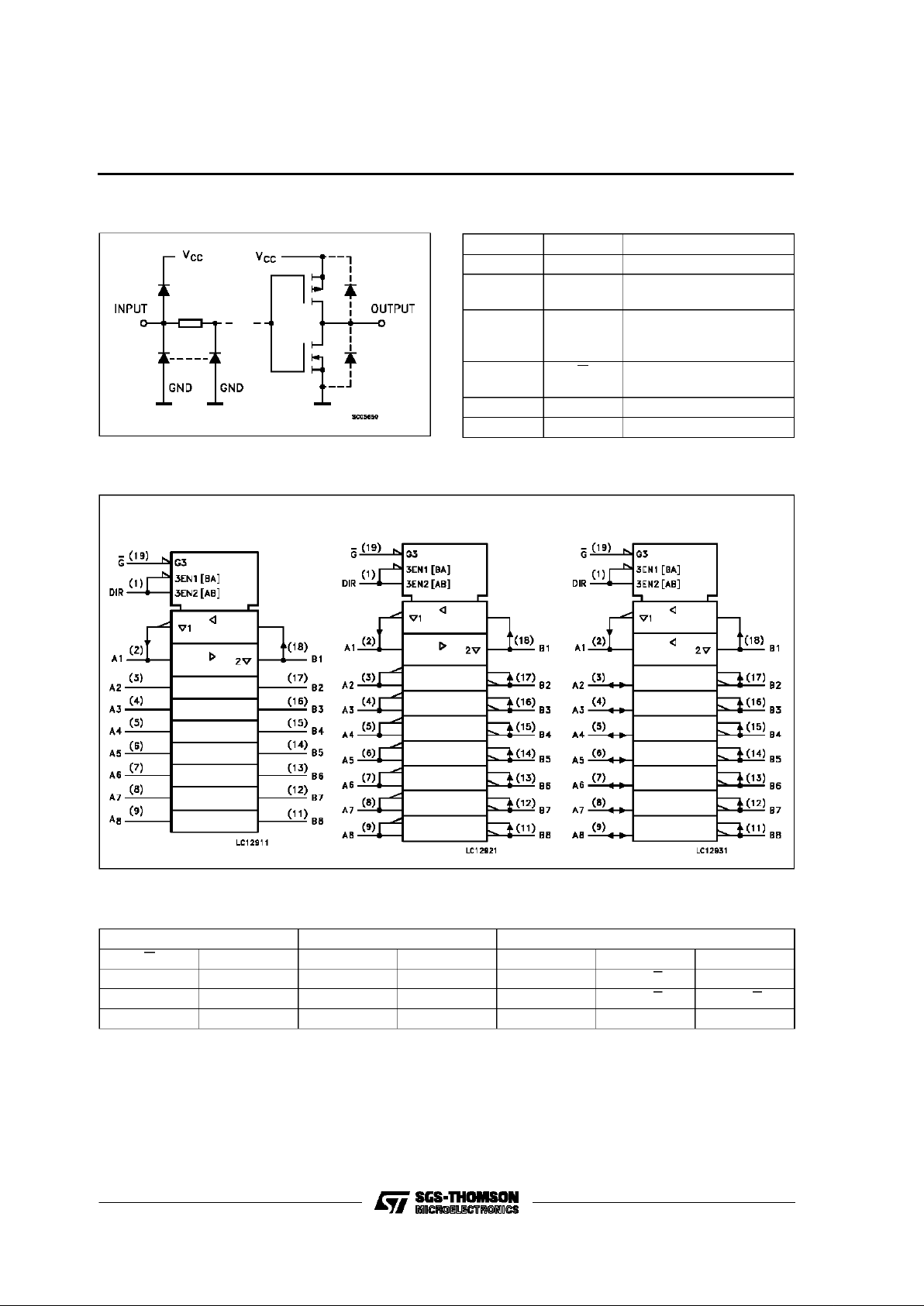
INPUT AND OUTPUT EQUIVALENT CIRCUIT PIN DESCRIPTION
PIN No SYMBOL NAME AND FUNCTION
1 DIR Directional Control
2, 3, 4, 5,
6, 7, 8, 9
A1 to A8 Data Inputs/Outputs
18, 17, 16,
15, 14, 13,
12, 11
B1 to B8 Data Inputs/Outputs
19 G Output Enabel Input
(Active LOW)
10 GND Ground (0V)
20 V
CC
Positive Supply Voltage
IEC LOGIC SYMBOLS
TRUTH TABLE
INPUT FUNCTION OUTPUT
G DIR A BUS B BUS HC245 HC640 HC643
L L OUTPUT INPUT A = B A = B A = B
L H INPUT OUTPUT B = A B = A B = A
HXZZZZZ
X: ”H” or ”L”
Z: Highimpedance
HC245 HC640 HC643
M54/M74HC245/640/643
2/11
Page 3
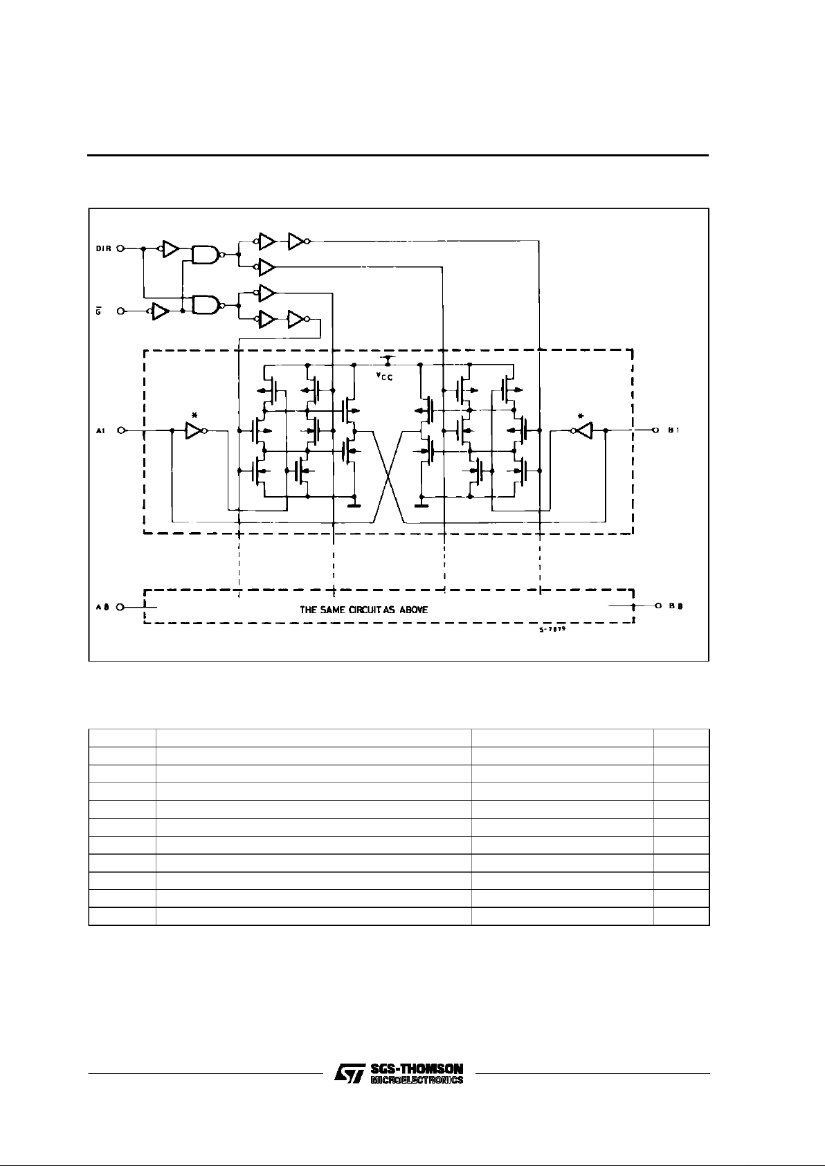
LOGIC DIAGRAM (HC640)
ABSOLU TE MAXIMUM RATING
Symbol Parameter Value Unit
V
CC
Supply Voltage -0.5 to +7 V
V
I
DC Input Voltage -0.5 to VCC+ 0.5 V
V
O
DC Output Voltage -0.5 to VCC+ 0.5 V
I
IK
DC Input Diode Current ± 20 mA
I
OK
DC Output Diode Current ± 20 mA
I
O
DC Output Source Sink Current Per Output Pin ± 35 mA
I
CC
or I
GND
DC VCCor Ground Current ± 70 mA
P
D
Power Dissipation 500 (*) mW
T
stg
Storage Temperature -65 to +150
o
C
T
L
Lead Temperature (10 sec) 300
o
C
AbsoluteMaximumRatingsarethosevaluesbeyondwhichdamagetothedevicemayoccur.Functional operationunder thesecondition isnotimplied.
(*)500 mW:≅ 65oC derateto300 mWby 10mW/oC: 65oCto85oC
NOTE:INCASE OF HC245 OR HC643, INPUTINVERTERS MARKED*AT ABUSAND B BUSARE ELIMINATEDRESPECTIVELY
M54/M74HC245/640/643
3/11
Page 4
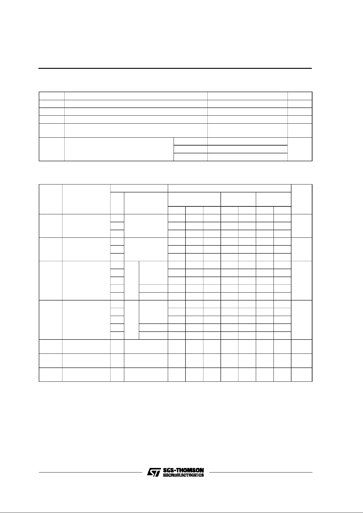
RECO MM ENDED OPERAT I N G CONDI TI O NS
Symbol Parameter Value Unit
V
CC
Supply Voltage 2 to 6 V
V
I
Input Voltage 0 to V
CC
V
V
O
Output Voltage 0 to V
CC
V
T
op
Operating Temperature: M54HC Series
M74HC Series
-55 to +125
-40 to +85
o
C
o
C
t
r,tf
Input Rise and Fall Time VCC= 2 V 0 to 1000 ns
V
CC
= 4.5 V 0 to 500
V
CC
= 6 V 0 to 400
DC SPECIFICATIO NS
Symbol Parameter
Test Conditions Value
Unit
V
CC
(V)
T
A
=25oC
54HC and 74HC
-40 to 85oC
74HC
-55 to 125oC
54HC
Min. Typ. Max. Min. Max. Min. Max.
V
IH
High Level Input
Voltage
2.0 1.5 1.5 1.5
V
4.5 3.15 3.15 3.15
6.0 4.2 4.2 4.2
V
IL
Low Level Input
Voltage
2.0 0.5 0.5 0.5
V
4.5 1.35 1.35 1.35
6.0 1.8 1.8 1.8
V
OH
High Level
Output Voltage
2.0
V
I
=
V
IH
or
V
IL
IO=-20 µA
1.9 2.0 1.9 1.9
V
4.5 4.4 4.5 4.4 4.4
6.0 5.9 6.0 5.9 5.9
4.5 I
O
=-6.0 mA 4.18 4.31 4.13 4.10
6.0 I
O
=-7.8 mA 5.68 5.8 5.63 5.60
V
OL
Low Level Output
Voltage
2.0
V
I
=
V
IH
or
V
IL
IO=20µA
0.0 0.1 0.1 0.1
V
4.5 0.0 0.1 0.1 0.1
6.0 0.0 0.1 0.1 0.1
4.5 I
O
= 6.0 mA 0.17 0.26 0.33 0.40
6.0 I
O
= 7.8 mA 0.18 0.26 0.33 0.40
I
I
Input Leakage
Current
6.0
VI=VCCor GND ±0.1 ±1 ±1 µA
I
OZ
3 State Output
Off State Current
6.0 VI=VIHor V
IL
VO=VCCor GND
±0.5 ±5.0 µA
I
CC
Quiescent Supply
Current
6.0 VI=VCCor GND 4 40 80 µA
M54/M74HC245/640/643
4/11
Page 5

AC ELECTRICAL CHARACTERISTICS (CL=50pF,Inputtr=tf=6ns)
Symbol Parameter
Test Conditions Value
Unit
V
CC
(V)
C
L
(pF)
T
A
=25oC
54HC and 74HC
-40 to 85oC
74HC
-55 to 125oC
54HC
Min. Typ. Max. Min. Max. Min. Max.
t
TLH
t
THL
Output Transition
Time
2.0
50
25 60 75 90
ns
4.5 7121918
6.0 6101315
t
PLH
t
PHL
Propagation
Delay Time
2.0
50
33 90 115 135
ns
4.5 12 18 23 27
6.0 10 15 20 23
2.0
150
48 120 150 180
ns
4.5 16 24 30 36
6.0 14 20 26 31
t
PZL
t
PZH
Output Enable
Time
2.0
50 RL=1KΩ
48 150 190 225
ns
4.5 16 30 38 45
6.0 14 26 32 38
2.0
150 R
L
=1KΩ
63 180 225 270
ns
4.5 21 36 45 54
6.0 18 31 38 46
t
PLZ
t
PHZ
Output Disable
Time
2.0
50 RL=1KΩ
37 150 190 225
ns
4.5 17 30 38 45
6.0 15 26 32 38
C
IN
Input Capacitance DIR, G 5 10 10 10 pF
C
I/OUT
Output
Capacitance
An, Bn 13
pF
C
PD
(*) Power Dissipation
Capacitance
HC245
HC640/643
39
37
pF
(*) CPDisdefined asthe value ofthe IC’s internalequivalent capacitance which is calculated fromthe operatingcurrent consumption without load.
(Referto TestCircuit).Average operting currentcan be obtained bythe followingequation. ICC(opr) = CPD•VCC•fIN+ICC/8(per circuit)
M54/M74HC245/640/643
5/11
Page 6

SWITCHING CHARACTERISTICS TEST WAVEFORM
TEST CIRCUIT ICC(Opr.) CPDCALCULATION
CPDis to be calculated with the following
formula by using the measured value of I
CC
(Opr.)in the test circuitopposite.
CPD=
I
CC
(
Opr
.)
fINxV
CC
M54/M74HC245/640/643
6/11
Page 7

Plastic DIP20 (0.25) MECHANICAL DATA
DIM.
mm inch
MIN. TYP. MAX. MIN. TYP. MAX.
a1 0.254 0.010
B 1.39 1.65 0.055 0.065
b 0.45 0.018
b1 0.25 0.010
D 25.4 1.000
E 8.5 0.335
e 2.54 0.100
e3 22.86 0.900
F 7.1 0.280
I 3.93 0.155
L 3.3 0.130
Z 1.34 0.053
P001J
M54/M74HC245/640/643
7/11
Page 8

Ceramic DIP20 MECHANICAL DATA
DIM.
mm inch
MIN. TYP. MAX. MIN. TYP. MAX.
A 25 0.984
B 7.8 0.307
D 3.3 0.130
E 0.5 1.78 0.020 0.070
e3 22.86 0.900
F 2.29 2.79 0.090 0.110
G 0.4 0.55 0.016 0.022
I 1.27 1.52 0.050 0.060
L 0.22 0.31 0.009 0.012
M 0.51 1.27 0.020 0.050
N1 4° (min.), 15° (max.)
P 7.9 8.13 0.311 0.320
Q 5.71 0.225
P057H
M54/M74HC245/640/643
8/11
Page 9

SO20 MECHANICAL DATA
DIM.
mm inch
MIN. TYP. MAX. MIN. TYP. MAX.
A 2.65 0.104
a1 0.10 0.20 0.004 0.007
a2 2.45 0.096
b 0.35 0.49 0.013 0.019
b1 0.23 0.32 0.009 0.012
C 0.50 0.020
c1 45° (typ.)
D 12.60 13.00 0.496 0.512
E 10.00 10.65 0.393 0.419
e 1.27 0.050
e3 11.43 0.450
F 7.40 7.60 0.291 0.299
L 0.50 1.27 0.19 0.050
M 0.75 0.029
S8°(max.)
P013L
M54/M74HC245/640/643
9/11
Page 10

PLCC20 MECHANICAL DATA
DIM.
mm inch
MIN. TYP. MAX. MIN. TYP. MAX.
A 9.78 10.03 0.385 0.395
B 8.89 9.04 0.350 0.356
D 4.2 4.57 0.165 0.180
d1 2.54 0.100
d2 0.56 0.022
E 7.37 8.38 0.290 0.330
e 1.27 0.050
e3 5.08 0.200
F 0.38 0.015
G 0.101 0.004
M 1.27 0.050
M1 1.14 0.045
P027A
M54/M74HC245/640/643
10/11
Page 11

Information furnished is believed to be accurate and reliable. However, SGS-THOMSON Microelectronics assumes no responsability for the
consequences of use of such information nor forany infringementofpatents or other rights of third parties which may results from its use. No
license isgrantedby implication orotherwiseunder any patentorpatent rights ofSGS-THOMSONMicroelectronics. Specificationsmentioned
in this publication are subject to change without notice. This publication supersedes and replaces all information previously supplied.
SGS-THOMSON Microelectronicsproductsare notauthorizedforuse ascritical componentsinlife supportdevices or systemswithout express
written approval of SGS-THOMSON Microelectonics.
1994 SGS-THOMSON Microelectronics - All Rights Reserved
SGS-THOMSON MicroelectronicsGROUPOF COMPANIES
Australia - Brazil - France - Germany - Hong Kong - Italy - Japan - Korea - Malaysia - Malta - Morocco - The Netherlands -
Singapore - Spain - Sweden - Switzerland - Taiwan - Thailand - UnitedKingdom - U.S.A
M54/M74HC245/640/643
11/11
 Loading...