

Page 1
.HIGH SPEED
f
= 60 MHz(TYP.) AT VCC=5V
MAX
.LOWPOWERDISSIPATION
ICC=4µA(MAX.) AT TA=25°C
.HIGH NOISEIMMUNITY
V
NIH=VNIL
=28%VCC(MIN.)
.OUTPUT DRIVE CAPABILITY
10 LSTTL LOADS
.SYMMETRICALOUTPUT IMPEDANCE
IOH =IOL= 4 mA (MIN.)
.BALANCEDPROPAGATION DELAYS
t
PLH=tPHL
.WIDE OPERATINGVOLTAGE RANGE
VCC(OPR)= 2V TO6 V
.PIN ANDFUNCTION COMPATIBLE
WITH 54/74LS597
M54HC597
M74HC597
8 BIT LATCH/SHIFT REGISTER
B1R
(PlasticPackage)
M1R
(MicroPackage)
ORDER CODES :
M54HC 597F1R M74H C597M1R
M74HC 597B1R M74HC5 97C1R
F1R
(CeramicPackage)
C1R
(Chip Carrier)
DESCRIPTION
The M54/74HC597 is a high speed CMOS 8-BIT
LATCH/SHIFT REGISTER fabricated insilicongate
C2MOStechnology. Ithasthesamehighspeedperformance of LSTTL combined with true CMOS low
powerconsumption.
Thisdevicescomesina16-pinpackageand consist
of an 8-bit storage latch feedinga parallel-in, serialout 8-bitshiftregister. Both thestorageregisterand
shift register have positive-edge triggered clocks.
The shift register also hasdirectload (fromstorage)
and clearinputs.
All inputs are equipped with protection circuits
against static discharge and transient voltage excess.
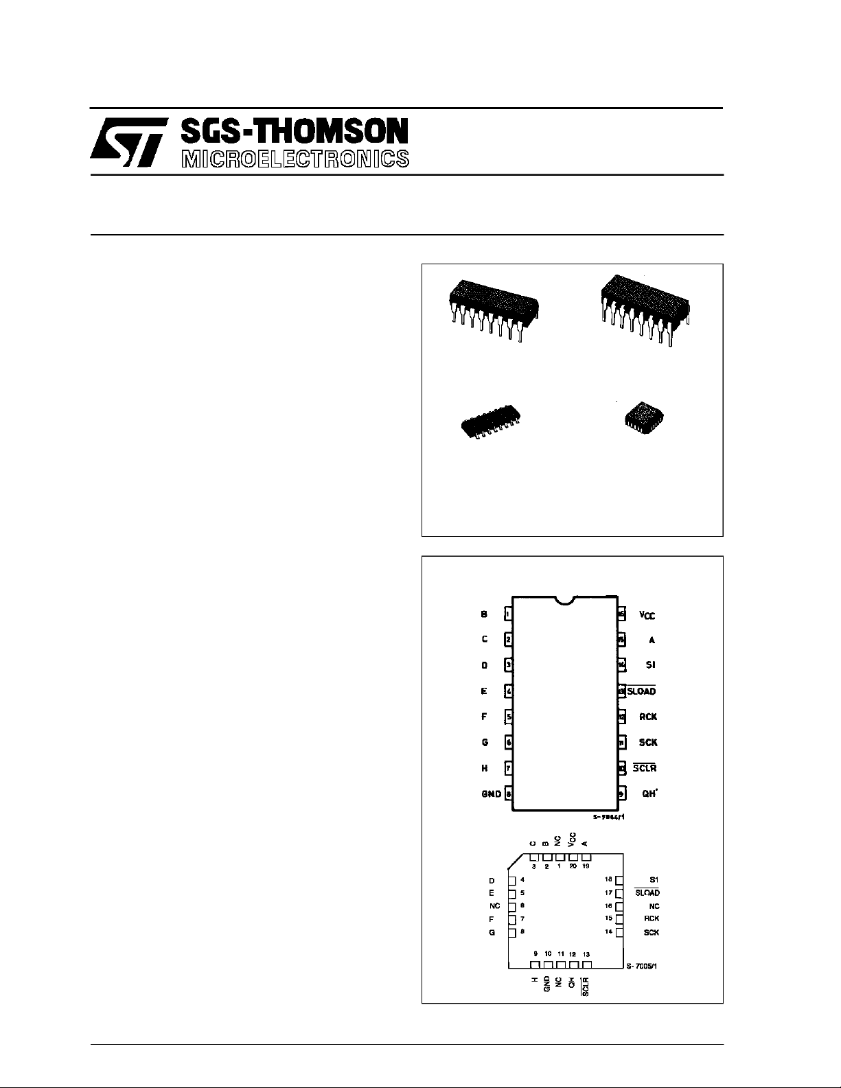
PIN CONNECTIONS(top view)
NC =
No Internal
Connection
October 1992
1/13
Page 2
M54/M74HC597
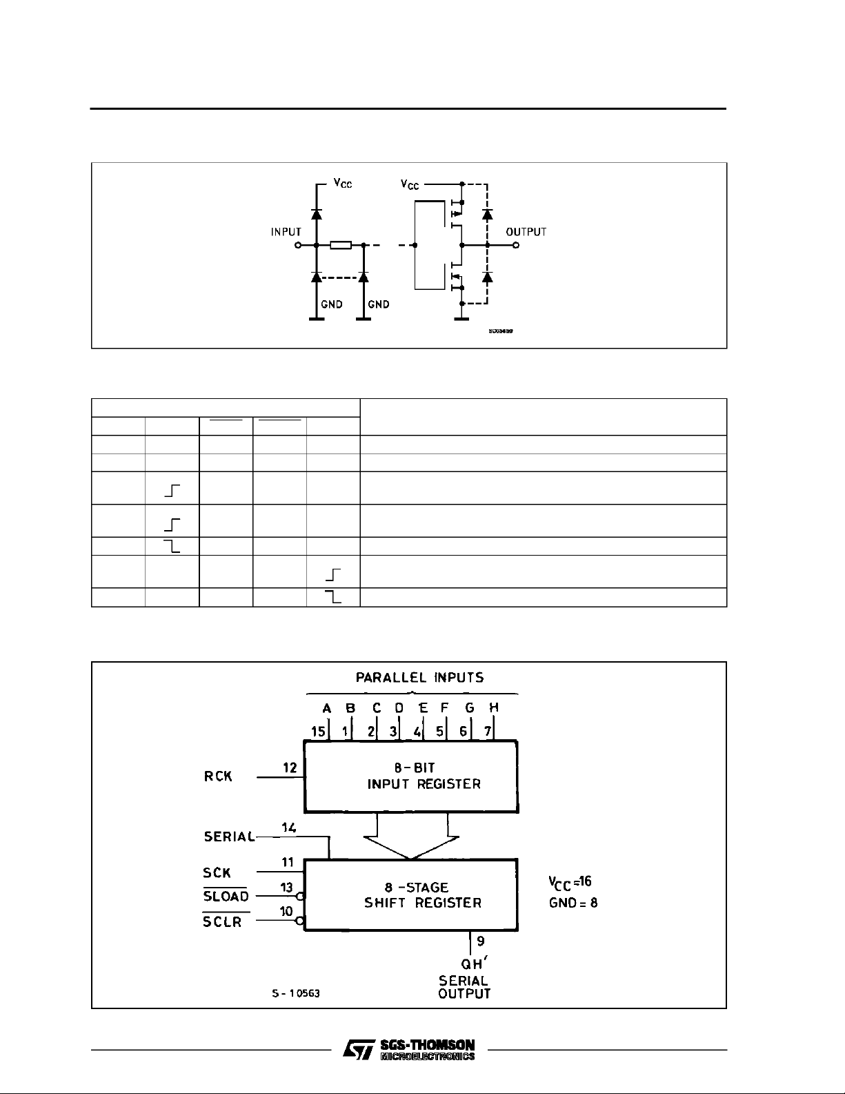
INPUT AND OUTPUT EQUIVALENT CIRCUIT
TRUTH TABLE
INPUTS
SI SCK SCLR SLOAD RCK
X X L H X S.R. IS CLEARED TO ”L”
X X H L X INPTU REGISTER DATA IS STORED INTO S.R.
L HHX
H HHX
X H H X STATE OF S.R IS NOT CHANGED
XXXX
X X X X STORAGE REGISTER STATE IS NOT CHANGED
X:DON’T CARE
FIRST STAGE OF S.R. BECOMES ”L” OTHER STAGES
STORE THE DATA OF PREVIOUS STAGE, RESPECTIVELY
FIRST STAGE OF S.R. BECOMES ”H” OTHER STAGES
STORE THE DATA OF PREVIOUS STAGE, RESPECTIVELY
INPUT DATA ON A ~ H LINE IS STORED INTO INPUT
REGISTER
OUTPUT
LOGIC DIAGRAM
2/13
Page 3
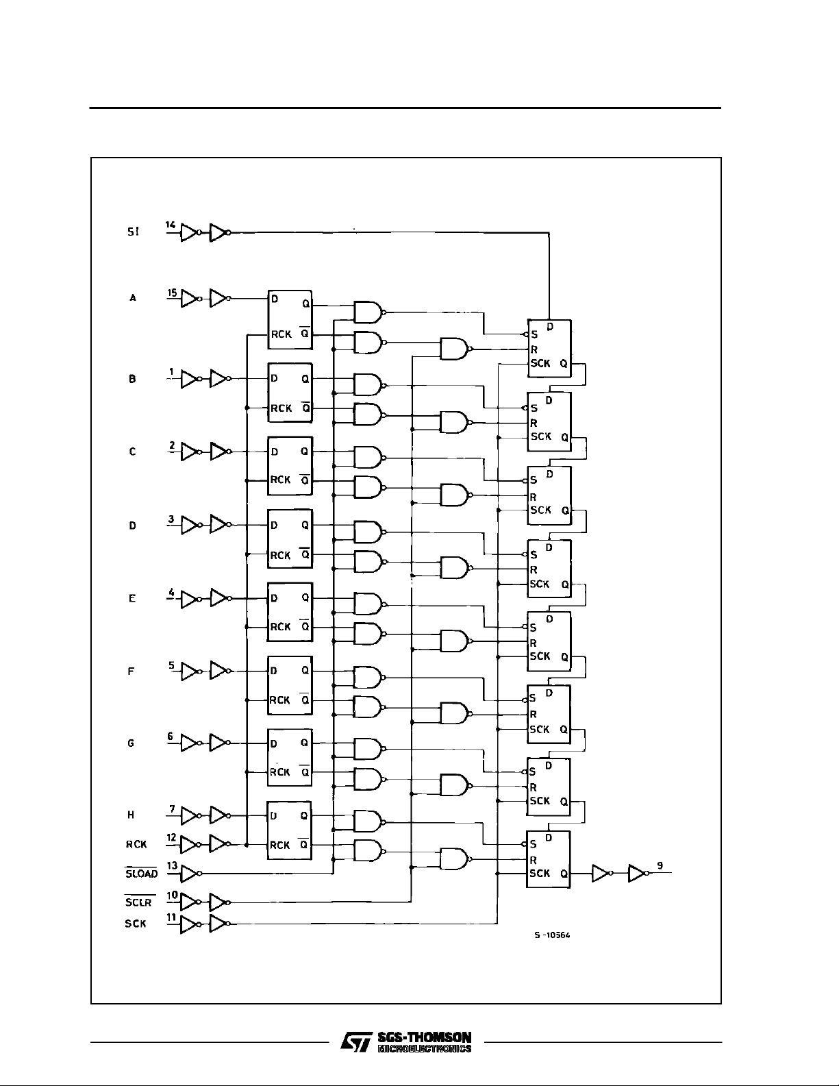
LOGIC DIAGRAM
M54/M74HC597
3/13
Page 4
M54/M74HC597
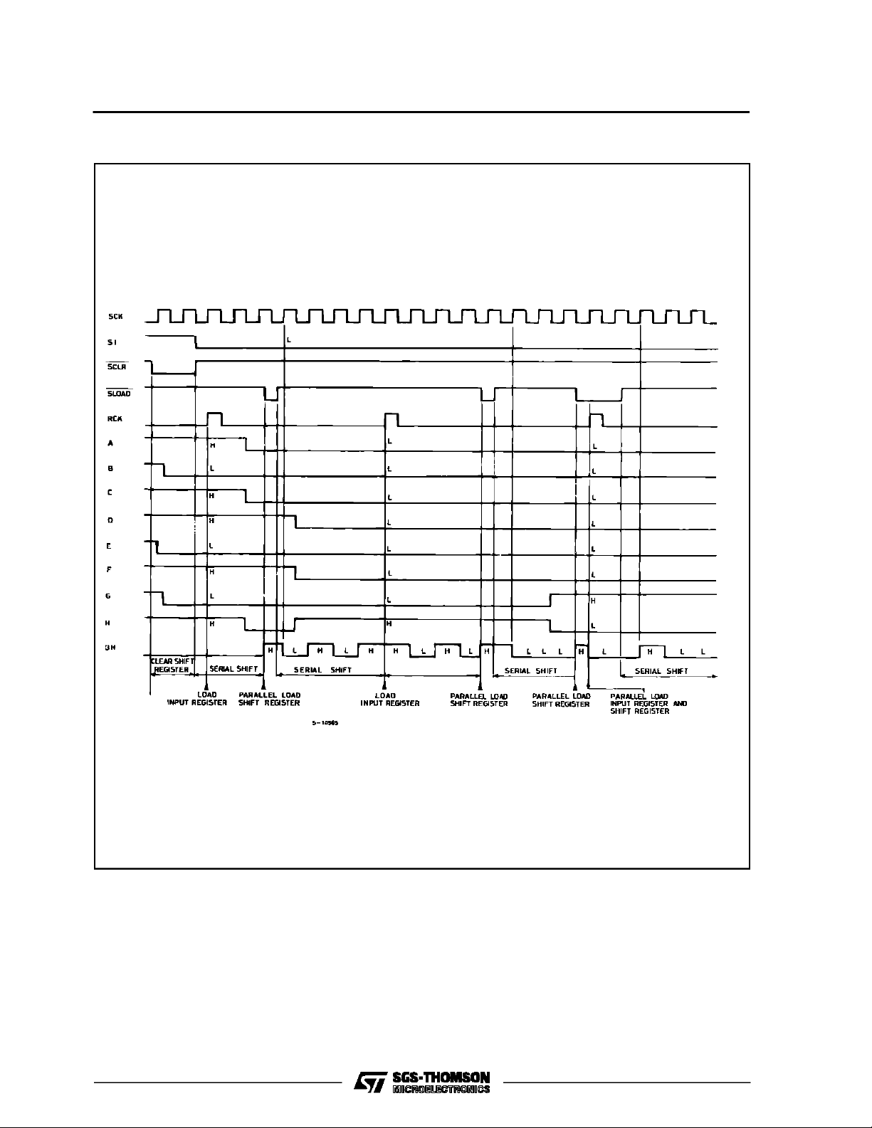
TIMING CHART
4/13
Page 5

M54/M74HC597
PIN DESC RIPTION
IEC LOGIC SYMBOL
PIN No SYMBOL NAME AND FUNCTION
9 QH’ Serial Data Outputs
10 SCLR Asynchronous Reset
Input (Active LOW)
11 SCK Shift Clock Input (LOW
to HIGH Edge-triggered)
12 RCK Storage Clock Input
(LOW to HIGH
Edge-triggered)
13 SLOAD Parallel Data Input
(Active LOW)
10 SI Serial Data Input
15, 1, 2, 3,
A to H Parallel Data Inputs
4, 5, 6, 7
8 GND Ground (0V)
16 V
CC
Positive Supply Voltage
ABSOLU TE M AXIMU M R AT INGS
Symbol Parameter Value Unit
V
CC
V
V
O
I
IK
I
OK
I
O
I
or I
CC
P
D
T
stg
T
AbsoluteMaximumRatingsarethose valuesbeyond whichdamage to thedevice mayoccur.Functional operation under these conditionisnotimplied.
(*)500 mW: ≅ 65oC derateto300 mWby 10mW/oC: 65oCto85oC
Supply Voltage -0.5 to +7 V
DC Input Voltage -0.5 to VCC+ 0.5 V
I
DC Output Voltage -0.5 to VCC+ 0.5 V
DC Input Diode Current ± 20 mA
DC Output Diode Current ± 20 mA
DC Output Source Sink Current Per Output Pin ± 25 mA
DC VCCor Ground Current ± 50 mA
GND
Power Dissipation 500 (*) mW
Storage Temperature -65 to +150
Lead Temperature (10sec) 300
L
o
C
o
C
RECO MM ENDED OPERAT I N G CO NDI TIONS
Symbol Parameter Value Unit
V
T
t
V
V
r,tf
Supply Voltage 2 to 6 V
CC
Input Voltage 0 to V
I
Output Voltage 0 to V
O
Operating Temperature: M54HC Series
op
M74HC Series
CC
CC
-55 to +125
-40 to +85
Input Rise and Fall Time VCC= 2 V 0 to 1000 ns
V
= 4.5 V 0 to 500
CC
V
= 6 V 0 to 400
CC
V
V
o
C
o
C
5/13
Page 6

M54/M74HC597
DC SPECIFICATIONS
Symbol Parameter
V
V
V
V
I
High Level Input
IH
Voltage
Low Level Input
IL
Voltage
High Level
OH
Output Voltage
Low Level Output
OL
Voltage
I
Input Leakage
I
Current
Quiescent Supply
CC
Current
Test Conditions Value
V
(V)
CC
=25oC
A
54HC and 74HC
Min. Typ. Max. Min. Max. Min. Max.
-40 to 85oC
74HC
-55 to 125oC
54HC
Unit
T
2.0 1.5 1.5 1.5
4.5 3.15 3.15 3.15
6.0 4.2 4.2 4.2
2.0 0.5 0.5 0.5
4.5 1.35 1.35 1.35
6.0 1.8 1.8 1.8
2.0
4.5 4.4 4.5 4.4 4.4
6.0 5.9 6.0 5.9 5.9
4.5 I
6.0 I
2.0
4.5 0.0 0.1 0.1 0.1
6.0 0.0 0.1 0.1 0.1
4.5 I
6.0 I
6.0
=
V
I
IO=-20 µA
V
IH
or
V
IL
=-4.0 mA 4.18 4.31 4.13 4.10
O
=-5.2 mA 5.68 5.8 5.63 5.60
O
V
=
I
IO=20µA
V
IH
or
V
IL
= 4.0 mA 0.17 0.26 0.33 0.40
O
= 5.2 mA 0.18 0.26 0.33 0.40
O
VI=VCCor GND ±0.1 ±1 ±1 µA
1.9 2.0 1.9 1.9
0.0 0.1 0.1 0.1
6.0 VI=VCCor GND 4 40 80 µA
V
V
V
V
AC ELECTRICAL CHARACTERISTICS (CL=50pF,Inputtr=tf=6ns)
Test Conditions Value
Symbol Parameter
t
TLH
t
THL
t
PLH
t
PHL
Output Transition
Time
Propagation
Delay Time
(SCK - QH’)
t
t
PLH
PHL
Propagation
Delay Time
(SCLR - QH’)
t
t
PLH
PHL
Propagation
Delay Time
(SLOAD - QH’)
t
t
PLH
PHL
Propagation
Delay Time
(RCK - QH’)
=25oC
T
V
(V)
CC
A
54HC and 74HC
Min. Typ. Max. Min. Max. Min. Max.
2.0 30 75 95 115
4.5 8151923
6.0 7131620
2.0 78 145 180 220
4.5 20 29 36 44
6.0 16 25 31 37
2.0 90 175 220 265
4.5 24 35 44 53
6.0 20 30 37 45
2.0 80 175 220 265
4.5 22 35 44 53
6.0 18 30 37 45
2.0
SLOAD = ”L”
4.5 30 42 53 63
112 210 265 315
6.0 24 36 45 54
-40 to 85oC
74HC
-55 to 125oC
54HC
Unit
ns
ns
ns
ns
ns
6/13
Page 7

M54/M74HC597
AC ELECTRICAL CHARACTERISTICS (CL=50pF,Inputtr=tf=6ns)
Test Conditions Value
T
=25oC
Symbol Parameter
f
MAX
Maximum Clock
Frequency
V
CC
(V)
2.0 6.0 12 4.8 4.0
4.5 30 48 24 20
A
54HC and 74HC
Min. Typ. Max. Min. Max. Min. Max.
6.0 35 50 28 24
t
W(H)
t
W(L)
Propagation
Delay Time
(SCK, RCK)
t
W(L)
Propagation
Delay Time
(SCLR, SLOAD)
Minimum Set-up
t
S
Time
(RCK - SLOAD)
Minimum Set-up
t
S
Time
(SI, SCK)
Minimum Set-up
t
S
Time
(PI - RCK)
Minimum Hold
t
f
Time
2.0 20 75 95 110
4.5 7151922
6.0 4131619
2.0 25 75 95 110
4.5 7151922
6.0 5131619
2.0 48 100 125 150
4.5 12 20 25 30
6.0 10 17 21 26
2.0 20 75 95 110
4.5 5151922
6.0 4131619
2.0 20 75 95 110
4.5 5151922
6.0 4131619
2.0 0 0 0
4.5 0 0 0
6.0 0 0 0
t
REM
C
C
PD
Propagation
Delay Time
(SCLR, SLOAD)
Input Capacitance 5 10 10 10 pF
IN
(*) Power Dissipation
2.0 12 75 95 115
4.5 4151923
6.0 3131620
60
Capacitance
(*) CPDisdefined as the value ofthe IC’sinternal equivalent capacitance which is calculated fromthe operatingcurrent consumption without load.
(Referto Test Circuit). Average operting current canbe obtained bythe followingequation. ICC(opr) = CPD•VCC•fIN+I
-40 to 85oC
74HC
-55 to 125oC
54HC
CC
Unit
ns
ns
ns
ns
ns
ns
ns
ns
pF
SWITCHING CHARACTERISTICS TEST WAVEFORM
7/13
Page 8

M54/M74HC597
TEST WAVEFORM (continued)
TEST CIRCUIT ICC(Opr.)
8/13
Page 9

Plastic DIP16 (0.25) MECHANICAL DATA
M54/M74HC597
DIM.
MIN. TYP. MAX. MIN. TYP. MAX.
a1 0.51 0.020
B 0.77 1.65 0.030 0.065
b 0.5 0.020
b1 0.25 0.010
D 20 0.787
E 8.5 0.335
e 2.54 0.100
e3 17.78 0.700
F 7.1 0.280
I 5.1 0.201
L 3.3 0.130
Z 1.27 0.050
mm inch
P001C
9/13
Page 10

M54/M74HC597
Ceramic DIP16/1 MECHANICAL DATA
DIM.
MIN. TYP. MAX. MIN. TYP. MAX.
A 20 0.787
B 7 0.276
D 3.3 0.130
E 0.38 0.015
e3 17.78 0.700
F 2.29 2.79 0.090 0.110
G 0.4 0.55 0.016 0.022
H 1.17 1.52 0.046 0.060
L 0.22 0.31 0.009 0.012
M 0.51 1.27 0.020 0.050
N 10.3 0.406
P 7.8 8.05 0.307 0.317
Q 5.08 0.200
mm inch
10/13
P053D
Page 11

SO16 (Narrow) MECHANICAL DATA
M54/M74HC597
DIM.
MIN. TYP. MAX. MIN. TYP. MAX.
A 1.75 0.068
a1 0.1 0.2 0.004 0.007
a2 1.65 0.064
b 0.35 0.46 0.013 0.018
b1 0.19 0.25 0.007 0.010
C 0.5 0.019
c1 45° (typ.)
D 9.8 10 0.385 0.393
E 5.8 6.2 0.228 0.244
e 1.27 0.050
e3 8.89 0.350
F 3.8 4.0 0.149 0.157
G 4.6 5.3 0.181 0.208
L 0.5 1.27 0.019 0.050
M 0.62 0.024
S8°(max.)
mm inch
P013H
11/13
Page 12

M54/M74HC597
PLCC20 MECHANICAL DATA
DIM.
MIN. TYP. MAX. MIN. TYP. MAX.
A 9.78 10.03 0.385 0.395
B 8.89 9.04 0.350 0.356
D 4.2 4.57 0.165 0.180
d1 2.54 0.100
d2 0.56 0.022
E 7.37 8.38 0.290 0.330
e 1.27 0.050
e3 5.08 0.200
F 0.38 0.015
G 0.101 0.004
M 1.27 0.050
M1 1.14 0.045
mm inch
12/13
P027A
Page 13

M54/M74HC597
Information furnishedis believed to be accurate and reliable. However, SGS-THOMSON Microelectronicsassumes no responsability for the
consequences of useof suchinformation nor for any infringement of patents or other rights of third parties which may results from its use. No
license is granted byimplication or otherwiseunder any patentor patentrights ofSGS-THOMSON Microelectronics.Specificationsmentioned
in this publication are subjectto changewithout notice. This publication supersedes andreplaces all information previouslysupplied.
SGS-THOMSON Microelectronicsproducts are not authorized foruse ascritical componentsin life supportdevices or systems without express
written approval of SGS-THOMSON Microelectonics.
1994SGS-THOMSON Microelectronics- All Rights Reserved
Australia -Brazil - France - Germany - Hong Kong - Italy - Japan - Korea - Malaysia - Malta -Morocco - The Netherlands-
Singapore -Spain - Sweden- Switzerland - Taiwan - Thailand- UnitedKingdom - U.S.A
SGS-THOMSON Microelectronics GROUP OFCOMPANIES
13/13
 Loading...