

Page 1
8 BIT BINARY COUNTER REGISTER (3 STATE)
.HIGH SPEED
f
= 62 MHz (TYP.) AT VCC=5V
MAX
.LOWPOWER DISSIPATION
ICC=4µA(MAX.) AT TA=25°C
.HIGH NOISE IMMUNITY
V
NIH=VNIL
=28%VCC(MIN.)
.OUTPUT DRIVE CAPABILITY
10 LSTTL LOADS (forRCO)
15 LSTTL LOADS (forQA ∼ QH)
.SYMMETRICAL OUTPUT IMPEDANCE
IOH=IOL= 6 mA(MIN.)FORQA~QHOUTPUT
IOH= IOL= 4 mA(MIN.) FOR RCO OUTPUT
.BALANCEDPROPAGATION DELAYS
t
PLH=tPHL
.WIDE OPERATING VOLTAGE RANGE
VCC(OPR)= 2 V TO 6 V
.PIN AND FUNCTION COMPATIBLE
WITH 54/74LS590
M54HC590
M74HC590
B1R
(PlasticPackage)
M1R
(MicroPackage)
ORDER CODES :
M54HC 590F1R M74H C590M1R
M74HC 590B1R M74HC5 90C1R
F1R
(CeramicPackage)
C1R
(Chip Carrier)
DESCRIPTION
The M54/74HC590 is a highspeedCMOS8-BITBINARY COUNTER REGISTER (3-STATE) fabricated in silicongate C2MOS technology.It hasthe
same high speed performance of LSTTLcombined
with true CMOS low power consumption.
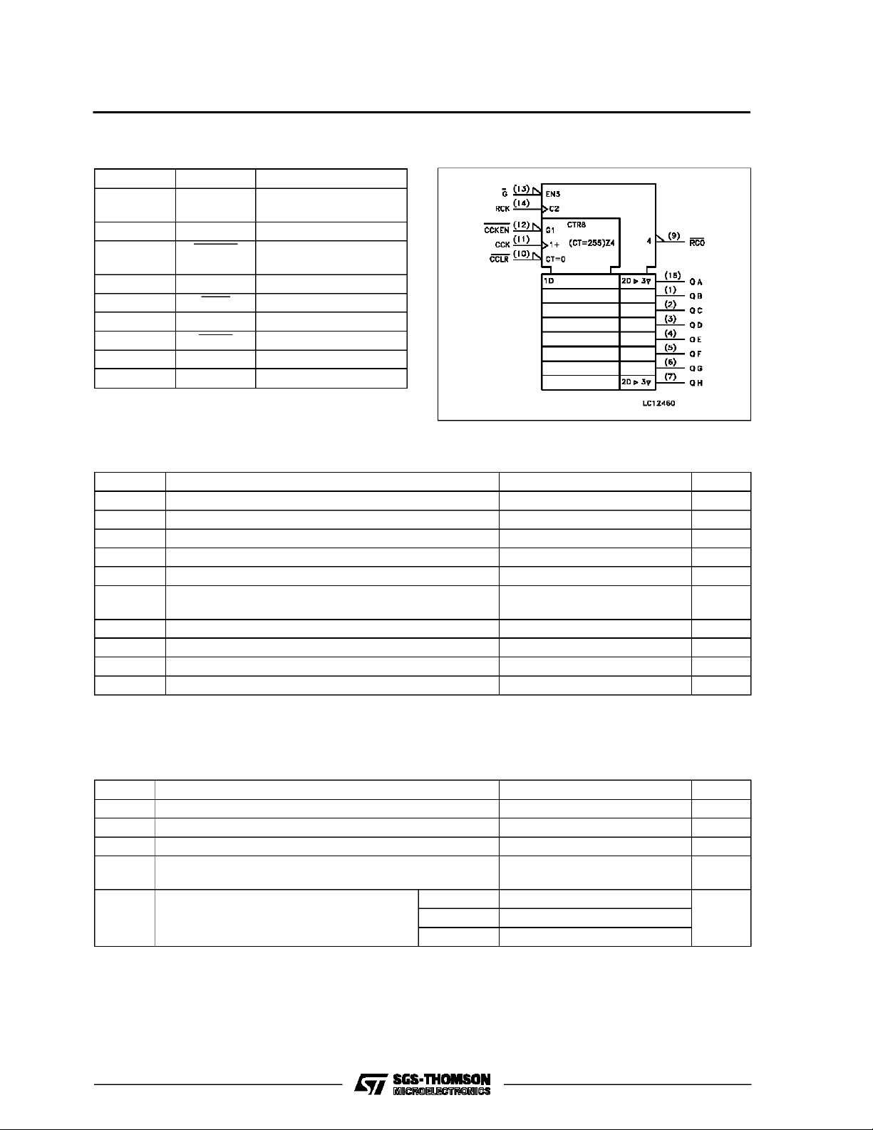
Thesedeviceseach contain an 8-bit binary counter
thatfeeds an8-bit storage register.Thestorageregister has parallel outputs. Separate clocks are provided for both the binary counter and storage
register. The binary counter features a direct clear
input CCLR and a count enable input CCKEN. For
cascading, a ripple carry output RCO is provided.
Expansion is easily accomplished by tying RCO of
the first stage to CCKEN of the second stage, etc.
Both the counter and register clocks are positiveedge triggered. If the user wishes to connect both
clockstogether, thecounter statewillalwaysbeone
count ahead of the register. Internal circuitry preventsclocking fromthe clock enable.
All inputs are equipped with protection circuits
against static discharge and transient excess voltage.
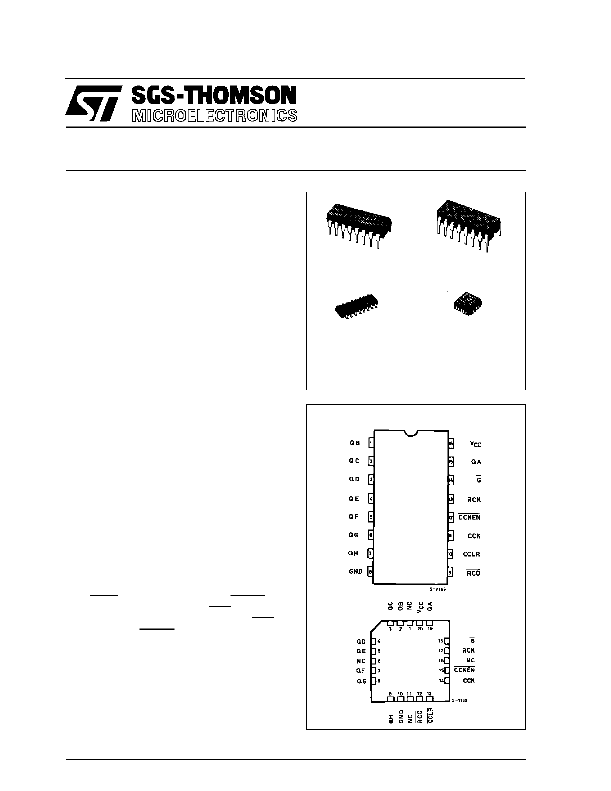
PIN CONNECTIONS(top view)
NC =
No Internal
Connection
March1993
1/14
Page 2
M54/M74HC590
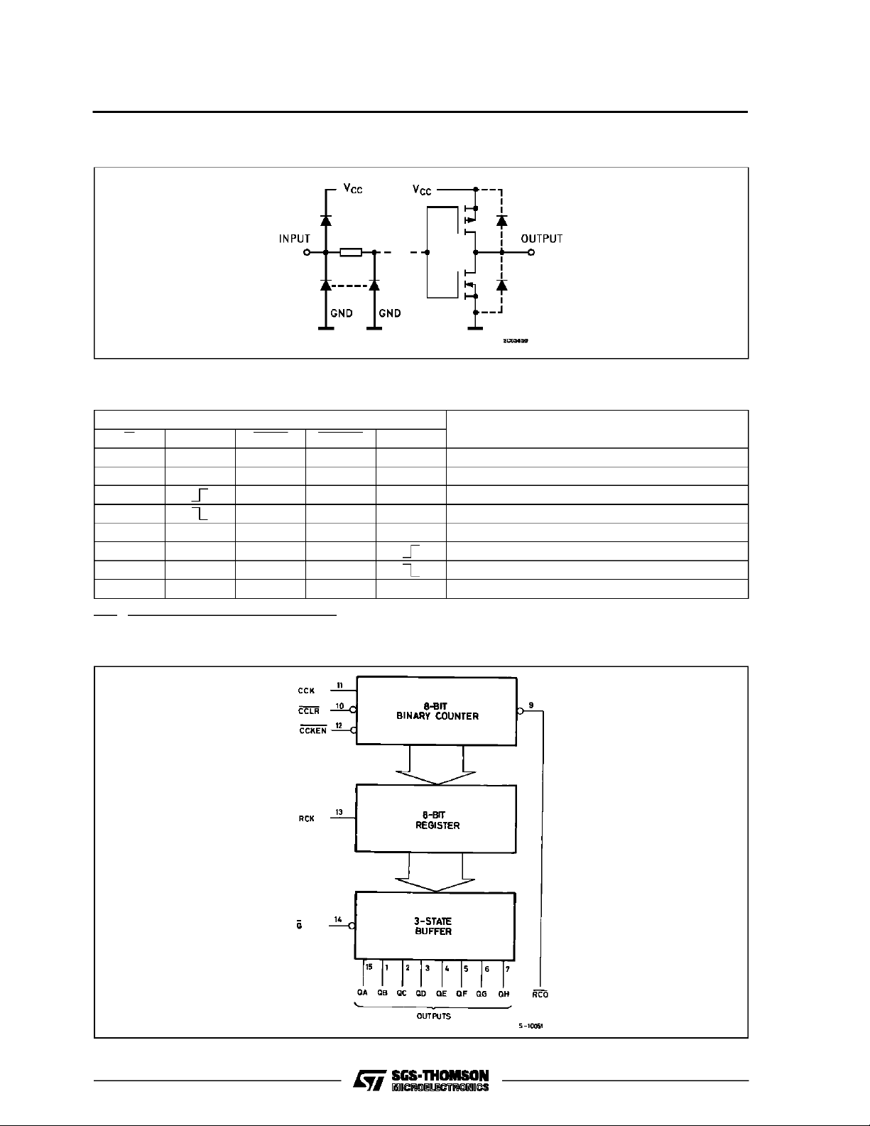
INPUT AND OUTPUT EQUIVALENT CIRCUIT
TRUTH TABLE
INPUTS
G RCK CCLR CCKEN CCK
H X X X X Q OUTPUTS DISABLE
L X X X X Q OUTPUTS ENABLE
X X X X COUNTER DATA IS STORED INTO REGISTER
X X X X REGISTER STATE IS NOT CHANGED
X X L X X COUNTER CLEAR
X X H L ADVANCE ONE COUNT
X X H L NO COUNT
X X H H X NO COUNT
X:DON’TCARE
RCO= QA’• QB’• QC’• QD’ • QE’ •QF’ • QG’• QH’ (QA’to QH’:INTERNALOUTPUTS OFTHE COUNTER)
OUTPUT
LOGIC DIAGRAM
2/14
Page 3
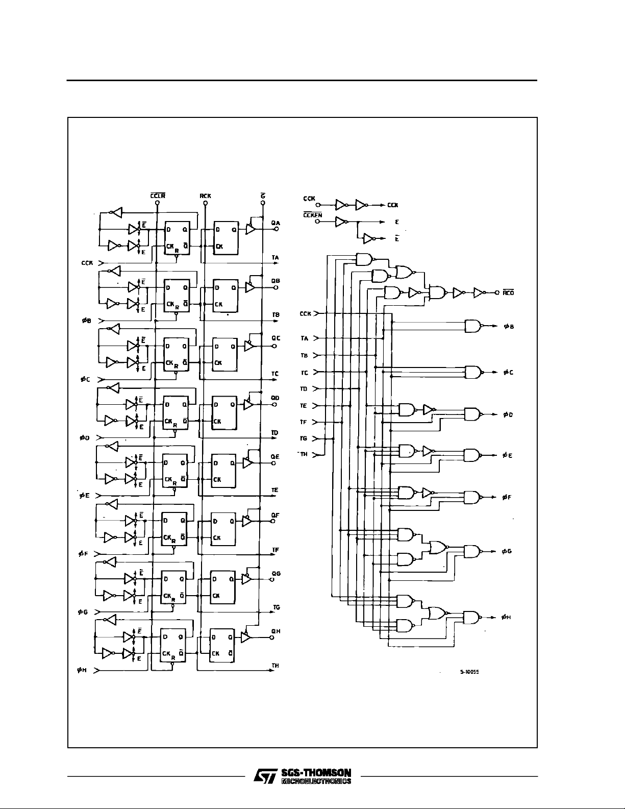
LOGIC DIAGRAM
M54/M74HC590
3/14
Page 4
M54/M74HC590
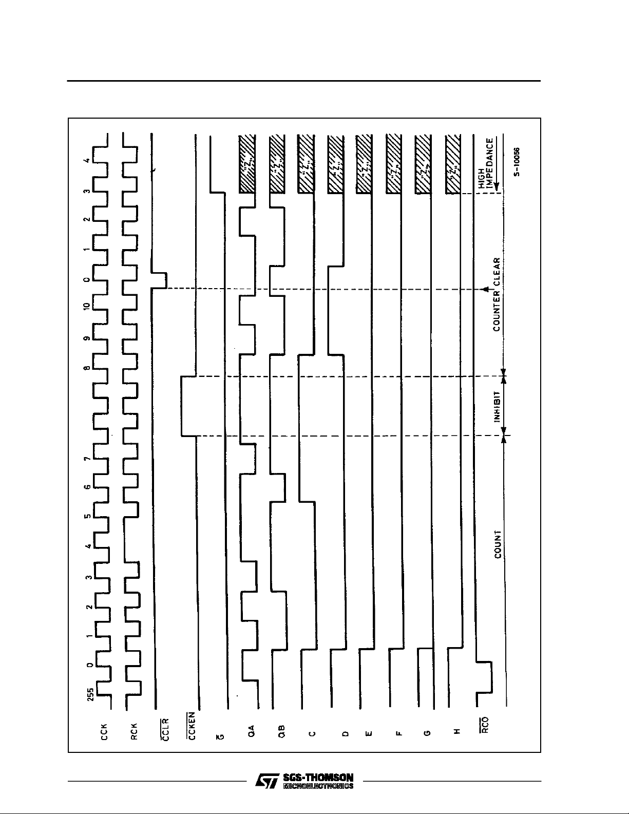
TIMING CHART
4/14
Page 5
M54/M74HC590
PIN DESCRIPTION
IEC LOGIC SYMBOL
PIN No SYMBOL NAME AND FUNCTION
1, 2, 3, 4, 5,
QA to QH Outputs
6, 7, 15
11 CCK Counter Clock Input
12 CCKEN Counter Clock Enable
Input
13 RCK Register Clock Input
9 RCO Ripple Carry Output
14 G Output Enable Input
10 CCLR Counter Clear Input
8 GND Ground (0V)
16 V
CC
Positive Supply Voltage
ABSOLU TE M AXIMU M R AT INGS
Symbol Parameter Value Unit
V
CC
V
V
O
I
IK
I
OK
I
O
I
or I
CC
P
D
T
stg
T
AbsoluteMaximumRatingsarethosevalues beyondwhichdamagetothedevicemayoccur. Functionaloperation under theseconditionisnotimplied.
(*)500 mW:≅ 65oC derate to300 mWby 10mW/oC: 65oCto85oC
Supply Voltage -0.5 to +7 V
DC Input Voltage -0.5 to VCC+ 0.5 V
I
DC Output Voltage -0.5 to VCC+ 0.5 V
DC Input Diode Current ± 20 mA
DC Output Diode Current ± 20 mA
DC Output Source Sink Current Per Output Pin (RCO)
(QA-QH)
DC VCCor Ground Current ± 70 mA
GND
±25
± 35
Power Dissipation 500 (*) mW
Storage Temperature -65 to +150
Lead Temperature (10 sec) 300
L
mA
o
o
C
C
RECO MM ENDED OPERAT I N G CO NDI TIONS
Symbol Parameter Value Unit
V
V
T
t
V
r,tf
Supply Voltage 2 to 6 V
CC
Input Voltage 0 to V
I
Output Voltage 0 to V
O
Operating Temperature: M54HC Series
op
M74HC Series
CC
CC
-55 to +125
-40 to +85
Input Rise and Fall Time VCC= 2 V 0 to 1000 ns
V
= 4.5 V 0 to 500
CC
V
= 6 V 0 to 400
CC
V
V
o
C
o
C
5/14
Page 6

M54/M74HC590
DC SPECIFICATIONS
Symbol Parameter
V
V
V
V
V
V
I
I
High Level Input
IH
Voltage
Low Level Input
IL
Voltage
High Level
OH
Output Voltage
(for RCO output)
High Level
OH
Output Voltage
(for QA to QH
outputs)
Low Level Output
OL
Voltage
(for RCO output)
Low Level Output
OL
Voltage
(for QA to QH
outputs)
I
Input Leakage
I
Current
3 State Output
OZ
Off State Current
Quiescent Supply
CC
Current
Test Conditions Value
V
(V)
CC
=25oC
A
54HC and 74HC
Min. Typ. Max. Min. Max. Min. Max.
-40 to 85oC
74HC
-55 to 125oC
54HC
Unit
T
2.0 1.5 1.5 1.5
4.5 3.15 3.15 3.15
6.0 4.2 4.2 4.2
2.0 0.5 0.5 0.5
4.5 1.35 1.35 1.35
6.0 1.8 1.8 1.8
2.0
4.5 4.4 4.5 4.4 4.4
6.0 5.9 6.0 5.9 5.9
4.5 I
6.0 I
2.0
4.5 4.4 4.5 4.4 4.4
6.0 5.9 6.0 5.9 5.9
4.5 I
6.0 I
2.0
4.5 0.0 0.1 0.1 0.1
6.0 0.0 0.1 0.1 0.1
4.5 I
6.0 I
2.0
4.5 0.0 0.1 0.1 0.1
6.0 0.0 0.1 0.1 0.1
4.5 I
6.0 I
6.0
6.0
=
V
I
IO=-20 µA
V
IH
or
V
IL
=-4.0 mA 4.18 4.31 4.13 4.10
O
=-5.2 mA 5.68 5.8 5.63 5.60
O
V
=
I
IO=-20 µA
V
IH
or
V
IL
=-6.0 mA 4.18 4.31 4.13 4.10
O
=-7.8 mA 5.68 5.8 5.63 5.60
O
=
V
I
IO=20µA
V
IH
or
V
IL
= 4.0 mA 0.17 0.26 0.33 0.40
O
= 5.2 mA 0.18 0.26 0.33 0.40
O
=
V
I
IO=20µA
V
IH
or
V
IL
= 6.0 mA 0.17 0.26 0.33 0.40
O
= 7.8 mA 0.18 0.26 0.33 0.40
O
VI=VCCor GND ±0.1 ±1 ±1 µA
VO=VCCor GND ±0.5 ±5 ±10 µA
1.9 2.0 1.9 1.9
1.9 2.0 1.9 1.9
0.0 0.1 0.1 0.1
0.0 0.1 0.1 0.1
6.0 VI=VCCor GND 4 40 80 µA
V
V
V
V
V
V
6/14
Page 7

AC ELECTRICAL CHARACTERISTICS (CL=50pF,Inputtr=tf=6ns)
Test Conditions Value
T
Symbol Parameter
t
TLH
t
THL
t
TLH
t
THL
t
PLH
t
PHL
Output Transition
Time (Qn)
Output Transition
Time (RCO)
Propagation
Delay Time
(CCK - RCO)
t
PLH
Propagation
Delay Time
(CCLR - RCO)
t
t
PLH
PHL
Propagation
Delay Time
(RCK - Q)
t
PZL
t
PZH
t
PLZ
t
PHZ
f
MAX
Output Enable
Time
Output Disable
Time
Maximum Clock
Frequency
t
W(L)
t
W(H)
Minimum Pulse
Width
(CCK, RCK)
t
W(L)
Minimum Pulse
Width
(CCLR)
t
Minimum Set-up
s
Time
(CCKEN - CCK)
=25oC
V
C
CC
(V)
L
(pF)
2.0
50
4.5 7121518
A
54HC and 74HC
Min. Typ. Max. Min. Max. Min. Max.
25 60 75 90
6.0 6101315
2.0
50
4.5 8151923
30 75 95 115
6.0 7131620
2.0
50
4.5 19 33 41 50
56 165 205 250
6.0 16 28 35 43
2.0
50
4.5 21 35 44 53
53 175 220 265
6.0 18 30 37 45
2.0
50
4.5 17 29 36 44
48 145 180 220
6.0 14 25 31 37
2.0
150
4.5 21 37 46 56
60 185 230 280
6.0 18 31 39 48
2.0
50 RL=1KΩ
4.5 13 21 26 32
39 105 130 160
6.0 11 18 22 27
2.0
150 R
4.5 17 27 34 41
=1KΩ
L
51 135 170 205
0 14232935
2.0
50 RL=1KΩ
4.5 14 21 26 32
28 105 130 160
6.0 12 18 22 27
2.0
50
4.5 33 52 26 22
6.6 13 5.2 4.4
6.0 39 61 31 26
2.0
50
4.5 9202529
36 100 125 145
6.0 8172125
2.0
50
4.5 8151922
32 75 95 110
6.0 7131619
2.0
50
4.5 11 20 25 30
44 100 125 150
6.0 9172126
-40 to 85oC
74HC
M54/M74HC590
-55 to 125oC
54HC
Unit
ns
ns
ns
ns
ns
ns
ns
ns
ns
ns
ns
ns
ns
7/14
Page 8

M54/M74HC590
AC ELECTRICAL CHARACTERISTICS (CL=50pF,Inputtr=tf=6ns)
Test Conditions Value
T
=25oC
Symbol Parameter
t
s(H)
Minimum Set-up
Time
(CCK - RCK)
t
Minimum Hold
h
Time
V
C
CC
(V)
L
(pF)
2.0
50
4.5 19 35 44 51
6.0 16 30 37 43
2.0
50
4.5 0 0 0
A
54HC and 74HC
Min. Typ. Max. Min. Max. Min. Max.
76 175 220 255
6.0 0 0 0
t
REM
C
C
PD
Minimum Hold
Time
(CCLR)
Input Capacitance 5 10 10 10 pF
IN
(*) Power Dissipation
2.0
50
4.5 7151922
28 75 95 110
6.0 6131619
40
Capacitance
(*) CPDisdefined asthe valueof the IC’s internal equivalent capacitance which is calculatedfrom the operatingcurrent consumption without load.
(RefertoTest Circuit).Average opertingcurrent can be obtained bythe followingequation. ICC(opr) = CPD•VCC•fIN+I
TEST WAVEFORM ICC(Opr.)
-40 to 85oC
74HC
-55 to 125oC
54HC
Unit
ns
000
ns
ns
pF
CC
8/14
Page 9

SWITCHING CHARACTERISTICS TEST WAVEFORM
M54/M74HC590
GND
V
CC
9/14
Page 10

M54/M74HC590
Plastic DIP16 (0.25) MECHANICAL DATA
DIM.
MIN. TYP. MAX. MIN. TYP. MAX.
a1 0.51 0.020
B 0.77 1.65 0.030 0.065
b 0.5 0.020
b1 0.25 0.010
D 20 0.787
E 8.5 0.335
e 2.54 0.100
e3 17.78 0.700
F 7.1 0.280
I 5.1 0.201
L 3.3 0.130
Z 1.27 0.050
mm inch
10/14
P001C
Page 11

Ceramic DIP16/1 MECHANICAL DATA
M54/M74HC590
DIM.
MIN. TYP. MAX. MIN. TYP. MAX.
A 20 0.787
B 7 0.276
D 3.3 0.130
E 0.38 0.015
e3 17.78 0.700
F 2.29 2.79 0.090 0.110
G 0.4 0.55 0.016 0.022
H 1.17 1.52 0.046 0.060
L 0.22 0.31 0.009 0.012
M 0.51 1.27 0.020 0.050
N 10.3 0.406
P 7.8 8.05 0.307 0.317
Q 5.08 0.200
mm inch
P053D
11/14
Page 12

M54/M74HC590
SO16 (Narrow) MECHANICAL DATA
DIM.
MIN. TYP. MAX. MIN. TYP. MAX.
A 1.75 0.068
a1 0.1 0.2 0.004 0.007
a2 1.65 0.064
b 0.35 0.46 0.013 0.018
b1 0.19 0.25 0.007 0.010
C 0.5 0.019
c1 45° (typ.)
D 9.8 10 0.385 0.393
E 5.8 6.2 0.228 0.244
e 1.27 0.050
e3 8.89 0.350
F 3.8 4.0 0.149 0.157
G 4.6 5.3 0.181 0.208
L 0.5 1.27 0.019 0.050
M 0.62 0.024
S8°(max.)
mm inch
12/14
P013H
Page 13

PLCC20 MECHANICAL DATA
M54/M74HC590
DIM.
MIN. TYP. MAX. MIN. TYP. MAX.
A 9.78 10.03 0.385 0.395
B 8.89 9.04 0.350 0.356
D 4.2 4.57 0.165 0.180
d1 2.54 0.100
d2 0.56 0.022
E 7.37 8.38 0.290 0.330
e 1.27 0.050
e3 5.08 0.200
F 0.38 0.015
G 0.101 0.004
M 1.27 0.050
M1 1.14 0.045
mm inch
P027A
13/14
Page 14

M54/M74HC590
Information furnished is believed to be accurate and reliable. However, SGS-THOMSON Microelectronicsassumes no responsability for the
consequences of use of such information nor for any infringement of patents or other rights of third parties which may results from its use. No
license isgranted by implication orotherwise underany patentor patent rights ofSGS-THOMSON Microelectronics. Specificationsmentioned
in this publication are subject to change without notice. This publication supersedes and replaces all information previously supplied.
SGS-THOMSON Microelectronicsproducts are notauthorizedforuse ascritical componentsin life support devicesor systemswithout express
written approval of SGS-THOMSON Microelectonics.
1994 SGS-THOMSON Microelectronics- All Rights Reserved
Australia - Brazil - France- Germany - HongKong - Italy - Japan - Korea - Malaysia - Malta - Morocco - The Netherlands-
Singapore - Spain - Sweden- Switzerland - Taiwan - Thailand - UnitedKingdom - U.S.A
SGS-THOMSON Microelectronics GROUP OF COMPANIES
14/14
 Loading...