

Page 1
HC4518 DUAL DECADE COUNTER
HC4520 DUAL 4 BIT BINARY COUNTER
.HIGH SPEED
f
= 55 MHz (TYP.) at VCC=5V
MAX
.LOWPOWER DISSIPATION
ICC=4µA(MAX.) AT TA=25°C
.HIGH NOISE IMMUNITY
V
NIH=VNIL
=28%VCC(MIN.)
.OUTPUT DRIVE CAPABILITY
10 LSTTL LOADS
.SYMMETRICAL OUTPUT IMPEDANCE
|IOH|=IOL=4 mA (MIN.)
.BALANCEDPROPAGATION DELAYS
t
PLH=tPHL
.WIDE OPERATING VOLTAGE RANGE
VCC(OPR)= 2 V TO6 V
.PIN AND FUNCTION COMPATIBLE WITH
4520B/4518B
M54/M74HC4518
M54/M74HC4520
B1R
(PlasticPackage)
M1R
(MicroPackage)
ORDER CODES :
M54HC XXXXF1R M74HCXXXXM1R
M74HC XXXXB1R M74HCXXXXC 1R
F1R
(CeramicPackage)
C1R
(Chip Carrier)
DESCRIPTION
The M54/74HC4518/4520 are high speed CMOS
DUAL 4 BIT BINARYCOUNTERSfabricated in silicon gate C2MOS technology. They have the same
high speed performance of LSTTL combined with
true CMOS low power consumption.
They consists of two identical internally synchronous 4-stagecounters. The counter stages are
D-type flip-flops having interchangeable Clock and
ENABLE inputsfor incrementing oneither the positive-goingor negative-going transition.
Forsingle-unit operation theENABLE inputismaintained ”high” and the counter advances on each
positive-going transition of the CLOCK. The
counters are cleared by high levels on their clear
lines. The counter can be cascaded in the ripple
mode by connecting Q4 to the enable input of the
subsequentcounter whiletheclockinput ofthe latter
is heldpermanently low.
All inputs are equipped with protection circuits
against static discharge and transient excess voltage.
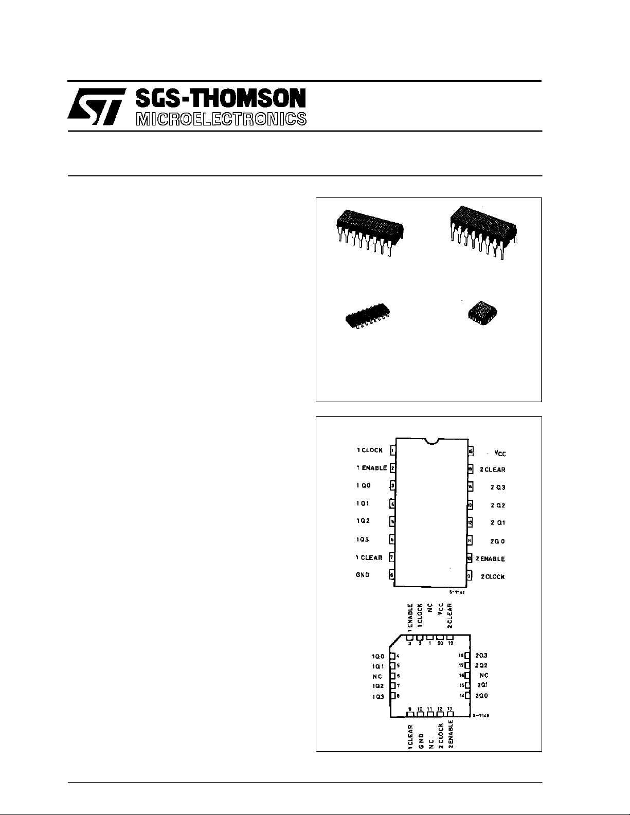
PIN CONNECTIONS(top view)
NC =
No Internal
Connection
March1993
1/13
Page 2
M54/M74HC4518/4520
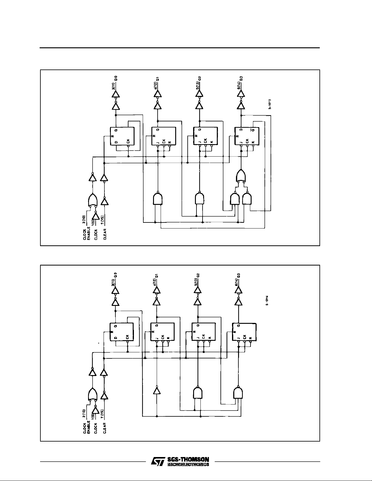
LOGIC DIAGRAM (1/2 HC4518)
LOGIC DIAGRAM (1/2 HC4520)
2/13
Page 3
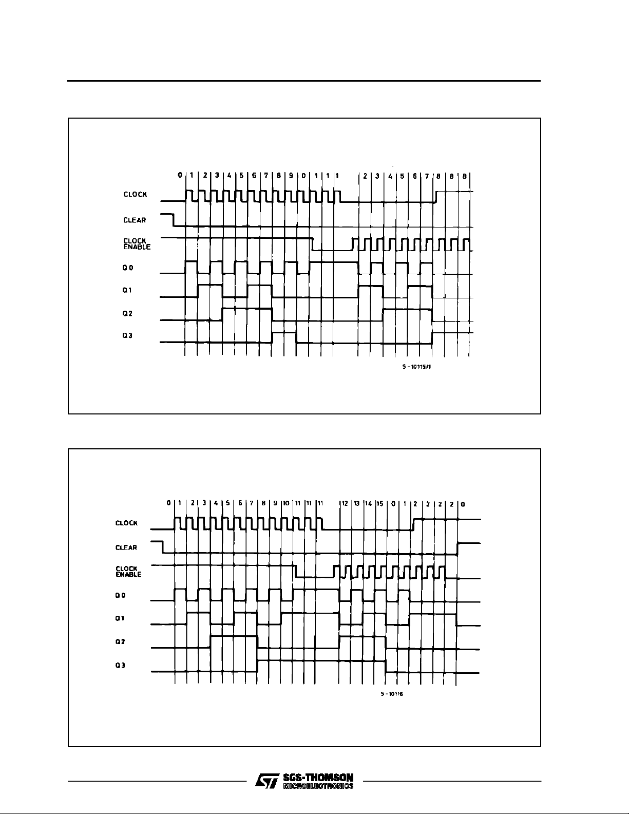
TIMING CHART (HC4518)
M54/M74HC4518/4520
TIMING CHART (HC4520)
3/13
Page 4
M54/M74HC4518/4520
TRUTH TABLE
INPUTS
CLOCK ENABLE CLEAR
H L INCREMENT COUNTER
L L INCREMENT COUNTER
X L NO CHANGE
X L NO CHANGE
L L NO CHANGE
H L NO CHANGE
X X H Q0 THRU Q3 = L
X:Don’tCare Z: HighImpedance
PIN No SYMBOL NAME AND FUNCTION
1, 9 1CLOCK,
2CLOCK
2, 10 1ENABLE,
2ENABLE
3, 4, 5, 6 1Q0 to 1Q3 Data Outputs
7, 15 1CLEAR,
2CLEAR
11, 12, 13,142Q0 to 2Q3 Data Outputs
Clock Inputs (LOW to
HIGH, Edge-triggered)
Clock Enable Inputs
Asynchronous Reset
Inputs (Active LOW)
FUNCTION
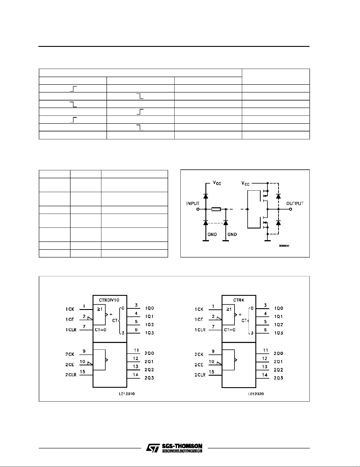
INPUT AND OUTPUT EQUIVALENT CIRCUITPIN DESCRIPTION
8 GND Ground (0V)
16 V
CC
IEC LOGIC SYMBOLS
HC4518 HC452 0
Positive Supply Voltage
4/13
Page 5

M54/M74HC4518/4520
ABSOLU TE MAXIMU M RAT INGS
Symbol Parameter Value Unit
V
CC
V
V
O
I
IK
I
OK
I
O
I
or I
CC
P
D
T
stg
T
AbsoluteMaximumRatings arethose values beyond whichdamagetothedevice mayoccur. Functionaloperationunder these conditionisnotimplied.
(*)500 mW:≅ 65oC derate to 300mW by 10mW/oC: 65oCto85oC
RECO MM ENDED OPERATIN G C O NDITIO NS
Symbol Parameter Value Unit
V
CC
V
I
V
O
T
op
t
r,tf
Supply Voltage -0.5 to +7 V
DC Input Voltage -0.5 to VCC+ 0.5 V
I
DC Output Voltage -0.5 to VCC+ 0.5 V
DC Input Diode Current ± 20 mA
DC Output Diode Current ± 20 mA
DC Output Source Sink Current Per Output Pin ± 25 mA
DC VCCor Ground Current ± 50 mA
GND
Power Dissipation 500 (*) mW
Storage Temperature -65 to +150
Lead Temperature (10 sec) 300
L
Supply Voltage 2 to 6 V
Input Voltage 0 to V
Output Voltage 0 to V
Operating Temperature: M54HC Series
M74HC Series
CC
CC
-55 to +125
-40 to +85
Input Rise and Fall Time VCC= 2 V 0 to 1000 ns
V
= 4.5 V 0 to 500
CC
V
= 6 V 0 to 400
CC
o
C
o
C
V
V
o
C
o
C
5/13
Page 6

M54/M74HC4518/4520
DC SPECIFICA TIONS
Symbol Parameter
V
V
V
V
I
High Level Input
IH
Voltage
Low Level Input
IL
Voltage
High Level
OH
Output Voltage
Low Level Output
OL
Voltage
I
Input Leakage
I
Current
Quiescent Supply
CC
Current
Test Conditions Value
V
(V)
CC
=25oC
A
54HC and 74HC
Min. Typ. Max. Min. Max. Min. Max.
-40 to 85oC
74HC
-55 to 125oC
54HC
Unit
T
2.0 1.5 1.5 1.5
4.5 3.15 3.15 3.15
6.0 4.2 4.2 4.2
2.0 0.5 0.5 0.5
4.5 1.35 1.35 1.35
6.0 1.8 1.8 1.8
2.0
4.5 4.4 4.5 4.4 4.4
6.0 5.9 6.0 5.9 5.9
4.5 I
6.0 I
2.0
4.5 0.0 0.1 0.1 0.1
6.0 0.0 0.1 0.1 0.1
4.5 I
6.0 I
6.0
=
V
I
IO=-20 µA
V
IH
or
V
IL
=-4.0 mA 4.18 4.31 4.13 4.10
O
=-5.2 mA 5.68 5.8 5.63 5.60
O
V
=
I
IO=20µA
V
IH
or
V
IL
= 4.0 mA 0.17 0.26 0.37 0.40
O
= 5.2 mA 0.18 0.26 0.37 0.40
O
VI=VCCor GND ±0.1 ±1 ±1 µA
1.9 2.0 1.9 1.9
0.0 0.1 0.1 0.1
6.0 VI=VCCor GND 4 40 80 µA
V
V
V
V
6/13
Page 7

M54/M74HC4518/4520
AC ELECTRICAL CHARACTERISTICS (CL=50pF,Inputtr=tf=6ns)
Test Conditions Value
T
=25oC
Symbol Parameter
t
t
TLH
THL
Output Transition
Time
V
CC
(V)
2.0 30 75 95 110
4.5 8151922
A
54HC and 74HC
Min. Typ. Max. Min. Max. Min. Max.
6.0 7131619
t
PLH
t
PHL
Propagation
Delay Time
(CK, CE - Qn)
t
PHL
Propagation
Delay Time
(CLR - Qn)
f
MAX
Maximum Clock
Frequency
2.0 72 160 200 240
4.5 22 32 40 48
6.0 18 27 34 41
2.0 65 150 190 225
4.5 20 30 38 45
6.0 16 26 33 38
2.0 6 23 4.8 4
4.5 30 51 24 20
6.0 35 60 28 24
t
W(H)
t
W(L)
Minimum Pulse
Width
(CK, CE)
t
W(L)
Minimum Pulse
Width
(CLR)
t
REM
Minimum
Removal Time
(CLR)
C
C
PD
Input Capacitance 5 10 10 10 pF
IN
(*) Power Dissipation
Capacitance
(*) CPDisdefined as the valueofthe IC’s internal equivalent capacitance whichis calculated from the operating currentconsumption withoutload.
(RefertoTest Circuit).Average operting currentcan be obtained bythe followingequation. ICC(opr) = CPD•VCC•fIN+ICC/2(per COUNTER)
2.0 25 75 95
4.5 6 15 19
6.0 5 13 16
2.0 20 75 95 110
4.5 5151922
6.0 4131619
2.0 21 50 60 75
4.5 3101215
6.0 3 9 11 13
for HC4518
for HC4520
38
32
-40 to 85oC
74HC
-55 to 125oC
54HC
Unit
ns
ns
ns
MHz
ns
ns
ns
pF
7/13
Page 8

M54/M74HC4518/4520
SWITCHING CHARACTERISTICS TEST WAVEFORMS
TEST CIRCUIT ICC(Opr.)
INPUT WAVEFORM IS THE SAME AS THAT IN CASE OF SWITCHING CHARACTERISTICS TESTS.
8/13
Page 9

M54/M74HC4518/4520
Plastic DIP16 (0.25) MECHANICAL DATA
DIM.
MIN. TYP. MAX. MIN. TYP. MAX.
a1 0.51 0.020
B 0.77 1.65 0.030 0.065
b 0.5 0.020
b1 0.25 0.010
D 20 0.787
E 8.5 0.335
e 2.54 0.100
e3 17.78 0.700
F 7.1 0.280
I 5.1 0.201
L 3.3 0.130
Z 1.27 0.050
mm inch
P001C
9/13
Page 10

M54/M74HC4518/4520
Ceramic DIP16/1 MECHANICAL DATA
DIM.
MIN. TYP. MAX. MIN. TYP. MAX.
A 20 0.787
B 7 0.276
D 3.3 0.130
E 0.38 0.015
e3 17.78 0.700
F 2.29 2.79 0.090 0.110
G 0.4 0.55 0.016 0.022
H 1.17 1.52 0.046 0.060
L 0.22 0.31 0.009 0.012
M 0.51 1.27 0.020 0.050
N 10.3 0.406
P 7.8 8.05 0.307 0.317
Q 5.08 0.200
mm inch
10/13
P053D
Page 11

SO16 (Narrow) MECHANICAL DATA
M54/M74HC4518/4520
DIM.
MIN. TYP. MAX. MIN. TYP. MAX.
A 1.75 0.068
a1 0.1 0.2 0.004 0.007
a2 1.65 0.064
b 0.35 0.46 0.013 0.018
b1 0.19 0.25 0.007 0.010
C 0.5 0.019
c1 45° (typ.)
D 9.8 10 0.385 0.393
E 5.8 6.2 0.228 0.244
e 1.27 0.050
e3 8.89 0.350
F 3.8 4.0 0.149 0.157
G 4.6 5.3 0.181 0.208
L 0.5 1.27 0.019 0.050
M 0.62 0.024
S8°(max.)
mm inch
P013H
11/13
Page 12

M54/M74HC4518/4520
PLCC20 MECHANICAL DATA
DIM.
MIN. TYP. MAX. MIN. TYP. MAX.
A 9.78 10.03 0.385 0.395
B 8.89 9.04 0.350 0.356
D 4.2 4.57 0.165 0.180
d1 2.54 0.100
d2 0.56 0.022
E 7.37 8.38 0.290 0.330
e 1.27 0.050
e3 5.08 0.200
F 0.38 0.015
G 0.101 0.004
M 1.27 0.050
M1 1.14 0.045
mm inch
12/13
P027A
Page 13

M54/M74HC4518/4520
Information furnished is believed to be accurate and reliable. However, SGS-THOMSON Microelectronics assumes no responsability for the
consequences of use of such information nor for any infringement of patents or other rights of third parties which may results from its use. No
license isgranted by implication orotherwise underany patentor patent rights ofSGS-THOMSON Microelectronics. Specificationsmentioned
in this publication are subject to change without notice. This publication supersedes and replaces all information previously supplied.
SGS-THOMSON Microelectronicsproducts are not authorizedforuse ascritical componentsinlife supportdevices or systems without express
written approval of SGS-THOMSON Microelectonics.
1994 SGS-THOMSON Microelectronics- All Rights Reserved
Australia - Brazil - France - Germany - Hong Kong - Italy - Japan - Korea - Malaysia - Malta - Morocco - The Netherlands -
Singapore - Spain - Sweden- Switzerland - Taiwan - Thailand - United Kingdom - U.S.A
SGS-THOMSON Microelectronics GROUP OF COMPANIES
13/13
 Loading...