

Page 1
BCD TO 7 SEGMENT LATCH/DECODER DRIVER
.HIGH SPEED
tPD= 28 ns(TYP.) AT VCC=5V
.LOWPOWER DISSIPATION
ICC=4µA(MAX.) AT TA=25°C
.HIGH NOISE IMMUNITY
V
NIH=VNIL
=28%VCC(MIN.)
.OUTPUT DRIVE CAPABILITY
10 LSTTLLOADS
.HIGH SOURGECURRENT
|IOH| =20 mA(MIN.)
.BALANCEDPROPAGATION DELAYS
t
PLH=tPHL
.WIDE OPERATINGVOLTAGE RANGE
VCC(OPR)= 2 V TO6 V
.PIN ANDFUNCTION COMPATIBLE
WITH 4511B
M54HC4511
M74HC4511
B1R
(PlasticPackage)
M1R
(MicroPackage)
ORDER CODES :
M54HC 4011F1R M74H C4011M1R
M74HC 4011B1R M74HC4 011C1R
F1R
(CeramicPackage)
C1R
(Chip Carrier)
DESCRIPTION
The M54/74HC4511 is a high speed CMOS BCDTO-7 SEGMENT LATCH/DECODER/DRIVER fabricated with silicon gate C2MOS technology. It
enables highspeedlatchanddecodeoperationwith
identical pin connection and function to standard
CMOS 4511B.
The segment output driver, which is CMOS fabricated in silicongate C2MOS technology, has large
IOHcapability whichenablescommon cathodeLeds
to be directly driven.
When lamp test(LT) is taken ”L”, all segment outputs will go to ”H”, and when blanking (BI) is taken
”L” and LT is taken ”H” allsegment outputswill go
to ”L”.
Thesefunctions operateregardless of other inputs
and are used to test the display.
Input BI isused to pulse-modulate the brightness of
the display.
When an errorinput code (over10)is appliedto the
BCD input,all segment outputs willgo ”L” (turn off).
All inputs are equipped with protection circuits
against static discharge and transient excess voltage.
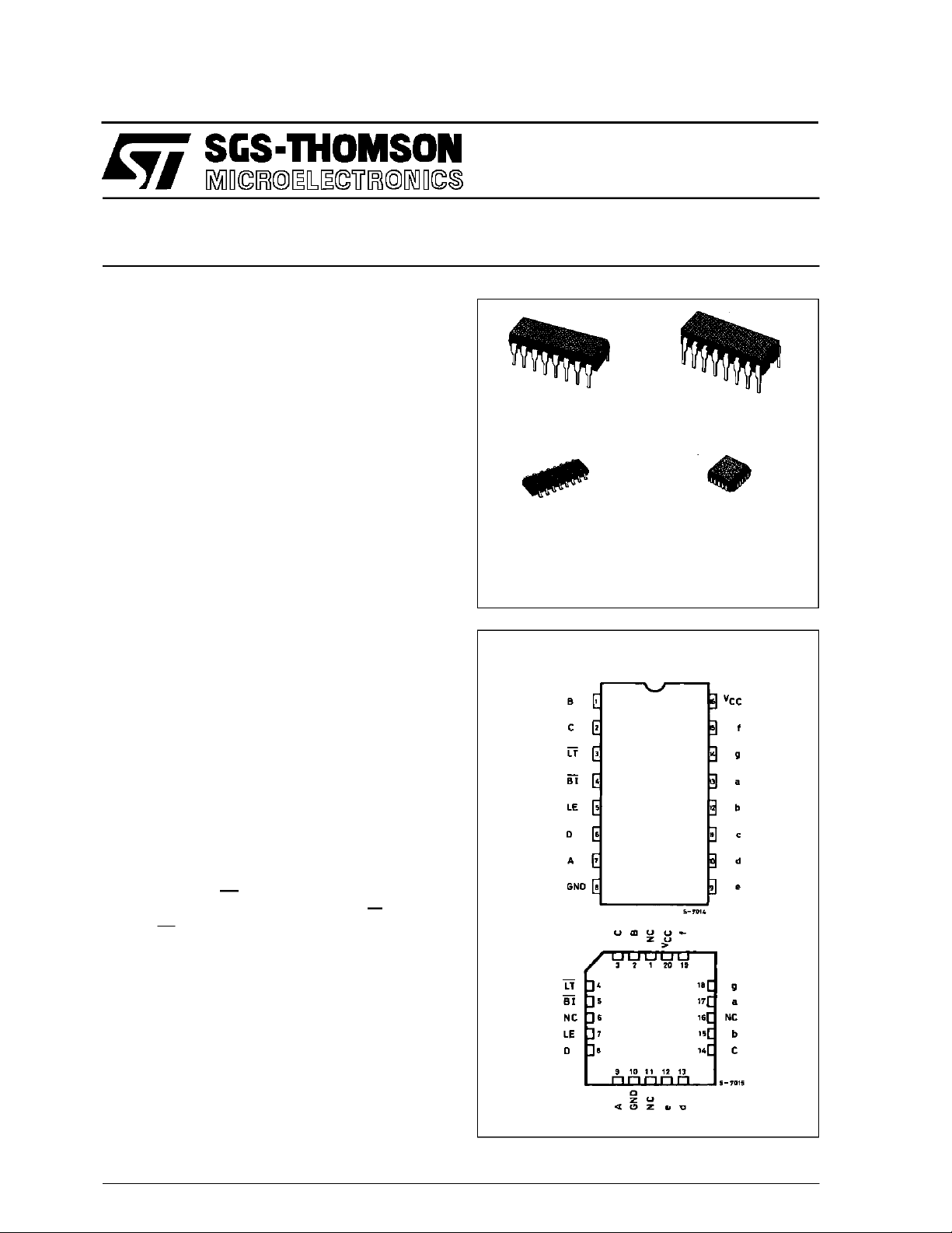
PIN CONNECTIONS (top view)
NC =
No Internal
Connection
February 1993
1/13
Page 2
M54/M74HC4511
TRUTH TABLE
INPUTS OUTPUTD DISPLAY
LE BI LT D C B A a b c d e f g
XXLXXXXHHHHHHH 8
XLHXXXXLLLLLLL BLANK
LHHLLLLHHHHHHL 0
LHHLLLHLHHLLLL 1
LHHLLHLHHLHHLH 2
LHHLLHHHHHHL LH 3
LHHLHLLLHHLLHH 4
LHHLHLHHLHHLHH 5
LHHLHHLLLHHHHH 6
LHHLHHHHHLLLLL 7
LHHHLLLHHHHHHH 8
LHHHLLHHHHL LHH 9
LHHHLHXLLLLLLL BLANK
LHHHHXXLLLLLLL BLANK
HHHXXXX Hold the stage at the leading edge of LE
X:Don’t Care
MODE
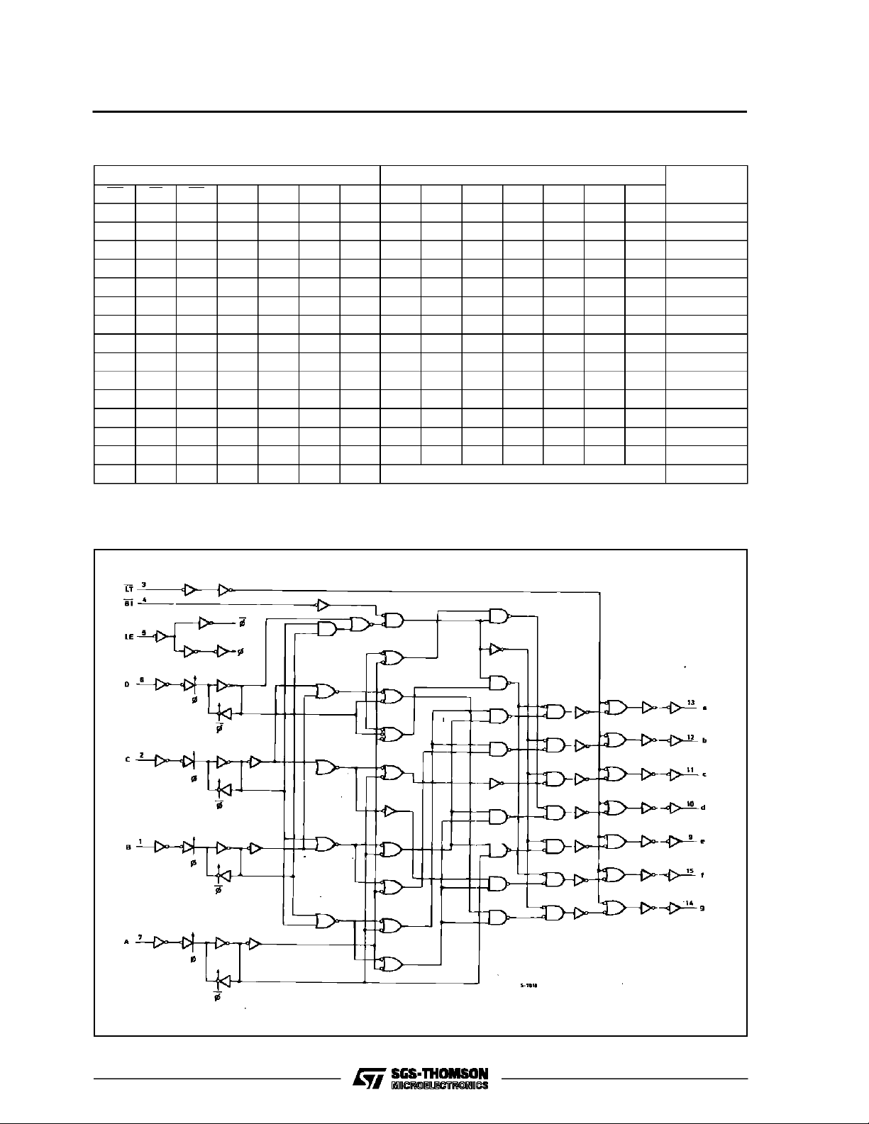
LOGIC DIAGRAM
2/13
Page 3
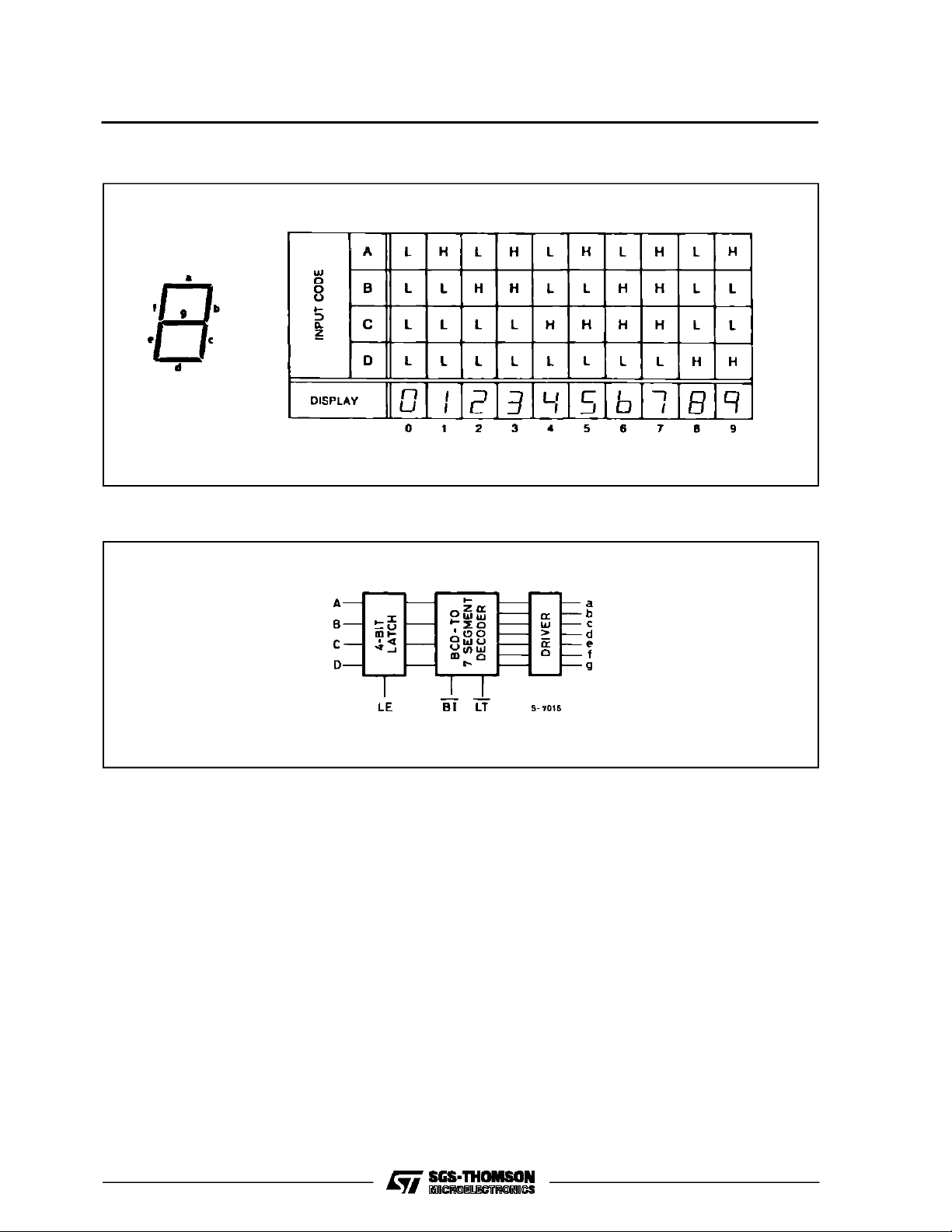
DISPLAY MODE
BLOCK DIAGRAM
M54/M74HC4511
3/13
Page 4
M54/M74HC4511
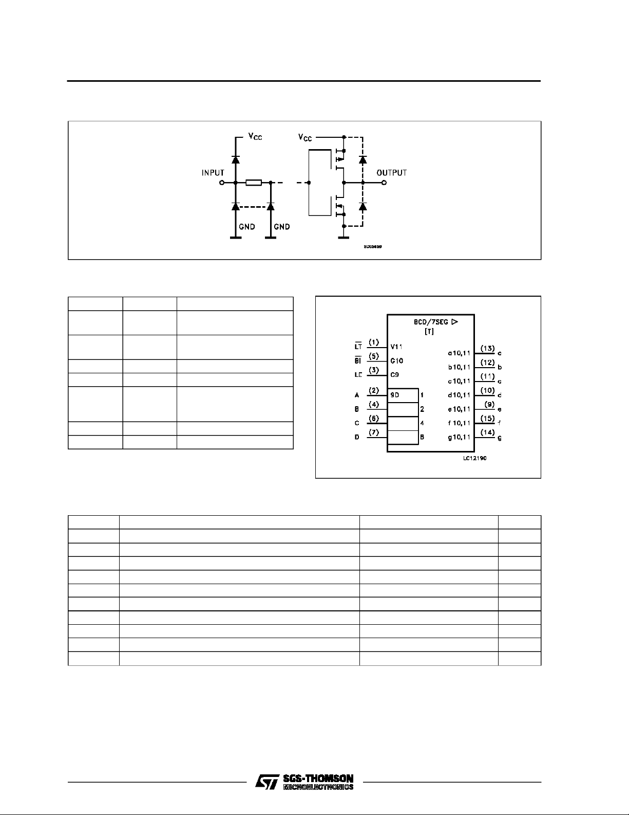
INPUT AND OUTPUT EQUIVALENT CIRCUIT
PIN DESCRIPTION
IEC LOGIC SYMBOL
PIN No SYMBOL NAME AND FUNCTION
3 LT Lamp Test Input (Active
LOW)
4 BI Ripple Blanking Input
(Active LOW)
5 LE Latch Enable Input
7, 1, 2, 6 A to D BCD Address Inputs
13, 12, 11,
a to g Segment Outputs
10, 9 , 15,
14
8 GND Ground (0V)
16 V
CC
Positive Supply Voltage
ABSOLU TE M AXI MU M R AT ING S
Symbol Parameter Value Unit
V
CC
V
V
O
I
IK
I
OK
I
O
I
or I
CC
P
D
T
stg
T
AbsoluteMaximumRatingsarethosevaluesbeyond whichdamagetothedevicemayoccur.Functional operationunder theseconditionisnotimplied.
(*)500 mW:≅ 65oC derateto 300 mWby 10mW/oC: 65oCto85oC
Supply Voltage -0.5 to +7 V
DC Input Voltage -0.5 to VCC+ 0.5 V
I
DC Output Voltage -0.5 to VCC+ 0.5 V
DC Input Diode Current ± 20 mA
DC OutputDiode Current ± 20 mA
DC Output Source Sink Current Per Output Pin -35/25 mA
DC VCCor Ground Current +150/-50 mA
GND
Power Dissipation 500 (*) mW
Storage Temperature -65 to +150
Lead Temperature (10 sec) 300
L
o
C
o
C
4/13
Page 5

M54/M74HC4511
RECO MM ENDED OPERAT I N G CO NDI TIONS
Symbol Parameter Value Unit
V
V
V
T
t
r,tf
DC SPECIFICATIO NS
Symbol Parameter
V
IH
V
V
OH
V
OL
I
I
CC
Supply Voltage 2 to 6 V
CC
Input Voltage 0 to V
I
Output Voltage 0 to V
O
Operating Temperature: M54HC Series
op
M74HC Series
CC
CC
-55 to +125
-40 to +85
Input Rise and Fall Time VCC= 2 V 0 to 1000 ns
V
= 4.5 V 0 to 500
CC
V
= 6 V 0 to 400
CC
Test Conditions Value
V
(V)
CC
=25oC
T
A
54HC and 74HC
-40 to 85oC
74HC
-55 to 125oC
Min. Typ. Max. Min. Max. Min. Max.
High Level Input
Voltage
2.0 1.5 1.5 1.5
4.5 3.15 3.15 3.15
6.0 4.2 4.2 4.2
Low Level Input
IL
Voltage
2.0 0.5 0.5 0.5
4.5 1.35 1.35 1.35
6.0 1.8 1.8 1.8
High Level
Output Voltage
Low Level Output
Voltage
Input Leakage
I
Current
Quiescent Supply
2.0
V
=
I
4.5 4.4 4.5 4.4 4.4
6.0 5.9 6.0 5.9 5.9
4.5 I
6.0 I
2.0
4.5 0.0 0.1 0.1 0.1
6.0 0.0 0.1 0.1 0.1
4.5 I
6.0 I
6.0
IO=-20 µA
V
IH
or
V
IL
=-4.0 mA 3.2 3.8 2.9
O
=-5.2 mA 5.68 5.8 5.63 5.60
O
V
=
I
IO=20µA
V
IH
or
V
IL
= 4.0 mA 0.17 0.26 0.37 0.40
O
= 5.2 mA 0.18 0.26 0.37 0.40
O
VI=VCCor GND ±0.1 ±1 ±1 µA
1.9 2.0 1.9 1.9
0.0 0.1 0.1 0.1
6.0 VI=VCCor GND 4 40 80 µA
Current
54HC
V
V
o
C
o
C
Unit
V
V
V
V
5/13
Page 6

M54/M74HC4511
AC ELECTRICAL CHARACTERISTICS (CL=50pF,Inputtr=tf=6ns)
Test Conditions Value
T
=25oC
Symbol Parameter
t
TLH
Output Transition
Time
V
CC
(V)
2.0 25 60 75 90
4.5 7121518
A
54HC and 74HC
Min. Typ. Max. Min. Max. Min. Max.
6.0 6111315
t
THL
Output Transition
Time
2.0 30 75 95 110
4.5 8151922
6.0 7131619
t
PLH
t
PHL
t
PLH
t
PHL
t
PLH
t
PHL
t
PLH
t
PHL
t
W(L)
Propagation
Delay Time
(BCD - Seg.)
Propagation
Delay Time
(BI - Seg.)
Propagation
Delay Time
(LT - Seg.)
Propagation
Delay Time
(LE - Seg.)
Minimum Pulse
Width
2.0 125 255 320 385
4.5 33 51 64 77
6.0 23 43 54 65
2.0 70 175 220 265
4.5 22 35 44 53
6.0 17 30 37 45
2.0 60 120 150 180
4.5 15 24 30 36
6.0 12 20 26 31
2.0 95 240 300 360
4.5 32 48 60 72
6.0 23 41 51 61
2.0 30 75 95 110
4.5 8151922
6.0 7131619
t
Minimum Set-up
s
Time
2.0 20 75 95 110
4.5 5151922
6.0 4131619
Minimum Hold
t
h
Time
2.0 0 0 0
4.5 0 0 0
6.0 0 0 0
C
C
PD
Input Capacitance 5 10 10 10 pF
IN
(*) Power Dissipation
95
Capacitance
(*) CPDisdefined as the valueof the IC’s internal equivalent capacitance which is calculated fromthe operatingcurrent consumption withoutload.
(Referto Test Circuit).Average opertingcurrentcan be obtained bythe followingequation. ICC(opr) = CPD•VCC•fIN+ICC/2(per FLIP/FLOP)
-40 to 85oC
74HC
-55 to 125oC
54HC
Unit
ns
ns
ns
ns
ns
ns
ns
ns
ns
pF
6/13
Page 7

SWITCHING CHARACTERISTICS TEST WAVEFORM
DataSegment Delay Time LE-Segment Delay Time
BI-Segment Delay Time LT-Segment Delay Time
M54/M74HC4511
DataSet-up/Hold Time
7/13
Page 8

M54/M74HC4511
TEST CIRCUIT ICC(Opr.)
APPLICATION CIRCUIT
StaticDisplay Circuit
8/13
Page 9

Plastic DIP16 (0.25) MECHANICAL DATA
M54/M74HC4511
DIM.
MIN. TYP. MAX. MIN. TYP. MAX.
a1 0.51 0.020
B 0.77 1.65 0.030 0.065
b 0.5 0.020
b1 0.25 0.010
D 20 0.787
E 8.5 0.335
e 2.54 0.100
e3 17.78 0.700
F 7.1 0.280
I 5.1 0.201
L 3.3 0.130
Z 1.27 0.050
mm inch
P001C
9/13
Page 10

M54/M74HC4511
Ceramic DIP16/1 MECHANICAL DATA
DIM.
MIN. TYP. MAX. MIN. TYP. MAX.
A 20 0.787
B 7 0.276
D 3.3 0.130
E 0.38 0.015
e3 17.78 0.700
F 2.29 2.79 0.090 0.110
G 0.4 0.55 0.016 0.022
H 1.17 1.52 0.046 0.060
L 0.22 0.31 0.009 0.012
M 0.51 1.27 0.020 0.050
N 10.3 0.406
P 7.8 8.05 0.307 0.317
Q 5.08 0.200
mm inch
10/13
P053D
Page 11

SO16 (Narrow) MECHANICAL DATA
M54/M74HC4511
DIM.
MIN. TYP. MAX. MIN. TYP. MAX.
A 1.75 0.068
a1 0.1 0.2 0.004 0.007
a2 1.65 0.064
b 0.35 0.46 0.013 0.018
b1 0.19 0.25 0.007 0.010
C 0.5 0.019
c1 45° (typ.)
D 9.8 10 0.385 0.393
E 5.8 6.2 0.228 0.244
e 1.27 0.050
e3 8.89 0.350
F 3.8 4.0 0.149 0.157
G 4.6 5.3 0.181 0.208
L 0.5 1.27 0.019 0.050
M 0.62 0.024
S8°(max.)
mm inch
P013H
11/13
Page 12

M54/M74HC4511
PLCC20 MECHANICAL DATA
DIM.
MIN. TYP. MAX. MIN. TYP. MAX.
A 9.78 10.03 0.385 0.395
B 8.89 9.04 0.350 0.356
D 4.2 4.57 0.165 0.180
d1 2.54 0.100
d2 0.56 0.022
E 7.37 8.38 0.290 0.330
e 1.27 0.050
e3 5.08 0.200
F 0.38 0.015
G 0.101 0.004
M 1.27 0.050
M1 1.14 0.045
mm inch
12/13
P027A
Page 13

M54/M74HC4511
Information furnished is believed to be accurate and reliable. However, SGS-THOMSON Microelectronics assumes no responsability for the
consequences of use of such information nor for any infringement of patents or other rights of third parties which may results from its use. No
license is granted byimplication or otherwise under any patent or patentrights of SGS-THOMSON Microelectronics. Specificationsmentioned
in this publication are subject to change without notice. This publication supersedes and replaces all information previously supplied.
SGS-THOMSON Microelectronicsproducts are not authorized foruse ascritical componentsin life support devices or systems without express
written approval of SGS-THOMSON Microelectonics.
1994 SGS-THOMSON Microelectronics - All Rights Reserved
Australia - Brazil - France - Germany - Hong Kong - Italy - Japan - Korea - Malaysia - Malta - Morocco - The Netherlands -
Singapore -Spain - Sweden- Switzerland -Taiwan - Thailand - UnitedKingdom - U.S.A
SGS-THOMSON Microelectronics GROUP OF COMPANIES
13/13
 Loading...