

Page 1
ANALOGMULTIPLE XER/D EMULTIPL EXER:
SIN GLE 8CH ANN EL, DUAL4CHAN NEL, TRIPLE2CH ANNEL
.LOW POWER DISSIPATION
ICC=4µA(MAX.) AT TA=25oC
.LOGICLEVEL TRANSLATION TO ENABLE 5V
LOGIC SIGNAL TO COMMUNICATE WITH
±5V ANALOGSIGNAL
.LOW ”ON” RESISTANCE:
70Ω TYP.(VCC-VEE= 4.5 V)
50Ω TYP.(VCC-VEE=9V)
.WIDEANALOGINPUTVOLTAGERANGE:±6V
.FAST SWITCHING:
tpd=15 ns(TYP.) AT TA=25oC
.LOWCROSSTALK BETWEEN SWITCHES
.HIGH ON/OFF OUTPUTVOLTAGE RATIO
.WIDE OPERATINGVOLTAGE RANGE
(VCC-VEE) = 2V TO 12V
.LOW SINE WAVE DISTORTION
0.02% AT VCC-VEE=9V
.HIGH NOISEIMMUNITY
V
NIH=VNIL
=28%VCC(MIN.)
.PIN AND FUNCTION COMPATIBLE WITH
HCC/HCF4051/4052/4053B
DESCRIPTION
These devices are analog multiplexer
demultiplexers in high speed silicon gate C2MOS
technology and they are pin compatible with the
equivalentmetalgateCMOS”4000B” series.These
analog switches are bidirectional and digitally
M54HC4051/52/53
M74HC4051/52/53
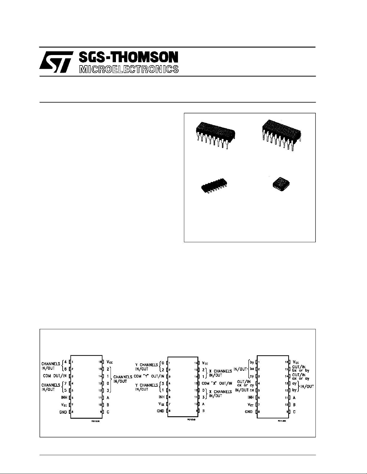
B1R
(PlasticPackage)
M1R
(MicroPackage)
ORDER CODE S :
M54HC XXXXF1 R M74H CX XXXM1R
M74HC XXXXB1R M74HCXXXXC1R
controlled.
A built-in level shifting isincluded to allowthem an
inputrange ofupto± 6V(peak) foran analog signal
with digital control signalof 0 to 6V.
VEEsupplypin is provided for analog input signals.
They have aninhibit (INH) input terminal to disable
allthe switcheswhen high. Foroperation as adigital
multiplexer/demultiplexer, VEEis connected to
GND.
F1R
(CeramicPackage)
C1R
(Chip Carrier)
PIN CONNECTION (top view)
October 1993
HC4053HC4052HC4 051
1/15
Page 2
M54/M74HC4051/4052/4053
DESCRIPTION
The HC4051 is a single 8 channel multiplexer
demultiplexer having threebinary control inputs A,
B and C to select 1 of 8 to be turned on, and
connected to the output.
The HC4052 has a pair of four channelmultiplexer
demultiplexer havingtwo controlinputsA and Bthat
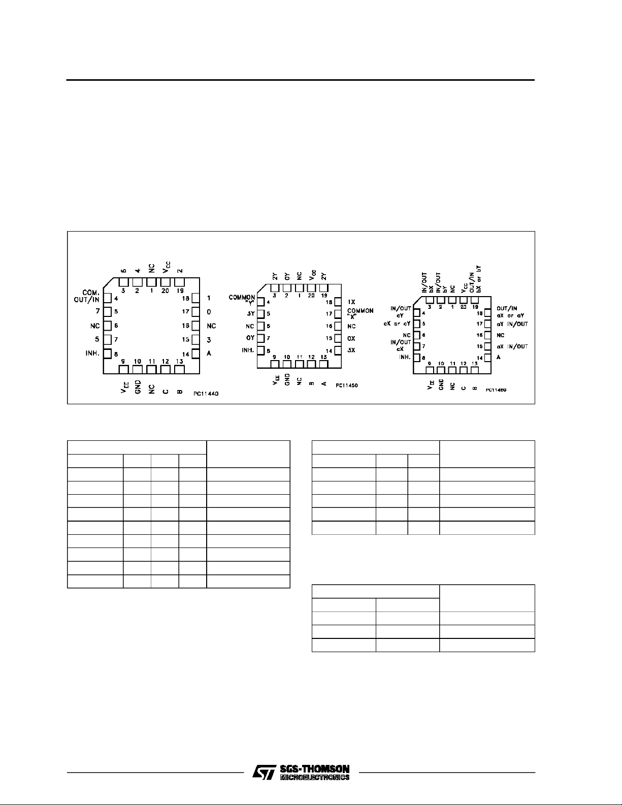
CHIP CARRIER
selectone offour channels of the two sections.
The HC4053 is a triple two channel multiplexer
demultiplexer havingthree separate digitalcontrol
inputs A,B and C toselect independently one of a
pairof channles.
HC4053HC405 2HC4051
TRUTH TABLE (HC4051)
INPUT STATES
INHIBIT C B A
LLLL 0
LLLH 1
LLHL 2
LLHH 3
LHLL 4
LHLH 5
LHHL 6
LHHH 7
H X X X NONE
X: DON’TCARE
”ON” CHANNEL
TRUTH TABLE (HC 4052)
INPUT STATES
INHIBIT B A
L L L 0X, 0Y
L L H 1X, 1Y
L H L 2X, 2Y
L H H 3X, 3Y
H X X NONE
X: DON’T CARE
TRUTH TABLE (HC 4053)
INPUT STATES
INHIBIT A or B or C
L L ax or bx or cx
L H ay or by or cy
H X NONE
X: DON’T CARE
”ON” CHANNELS
”ON” CHANNELS
2/15
Page 3
IEC LOGIC SYMBOLS
M54/M74HC4051/4052/4053
HC405 3HC4052HC4051
PIN DESCRIPTION (H C4051)
PIN No SYMBOL NAME AND FUNCTION
3 COM
Common Output/input
OUT/IN
6 INH INHIBIT Input
7V
EE
Negative Supply Voltage
11, 10, 9 A, B, C Select Inputs
13, 14, 15,
0 TO 7 Independent Input/Outputs
12, 1, 5, 2, 4
8 GND Ground (0V)
16 V
CC
Positive Supply Voltage
PIN DESCRIPTION (H C4053)
PIN No SYMBOL NAME AND FUNCTION
2, 1 bx, by Independent Input/Outputs
5, 3 cx, cy IndependentInput/Outputs
6 INH INHIBIT Input
7V
EE
11, 10, 9 A, B, C Select Inputs
12, 13 ax, ay Independent Input/Outputs
14, 15, 4 ax TO cy Common Output/input
8 GND Ground (0V)
16 V
CC
Negative Supply Voltage
Positive Supply Voltage
PIN DESCRIPTI ON (HC 4052)
PIN No SYMBOL NAME AND FUNCTION
1, 5, 2, 4 0Y TO 3Y Independent Input/Outputs
6 INH INHIBIT Input
7V
EE
10, 9 A, B Select Inputs
12, 14, 15,110X TO 3X Independent Input/Outputs
3 COM Y
OUT/IN
13 COM X
OUT/IN
8 GND Ground (0V)
16 V
CC
Negative Supply Voltage
Common X Output/input
Common Y Output/input
Positive Supply Voltage
3/15
Page 4
M54/M74HC4051/4052/4053
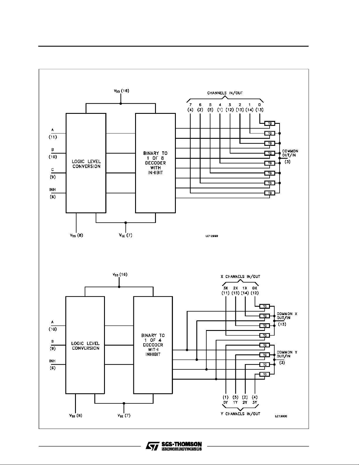
FUNCTIONAL DIAGRAM
HC4051
HC4052
4/15
Page 5
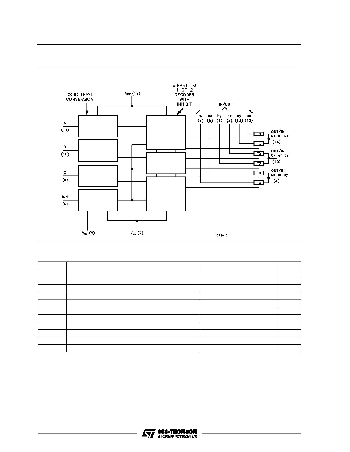
FUNCTIONAL DIAGRAM
HC4053
M54/M74HC4051/4052/4053
ABSOLU TE M AXI MUM RATING S
Symbol Parameter Value Unit
V
CC
V
CC-VEE
V
IN
V
I/O
I
CK
I
IOK
I
T
I
CC
P
T
stg
T
AbsoluteMaximumRatingsarethosevalues beyond whichdamagetothedevicemayoccur. Functionaloperation undertheseconditionsis not implied.
(*)500 mW: ≅ 65oC derateto300 mWby 10mW/oC: 65oCto85oC
Supply Voltage Range -0.5 to +7 V
Supply Voltage Range -0.5 to 13 V
Control Input Voltage -0.5 to VCC+ 0.5 V
Switch I/O Voltage VEE- 0.5 to VCC+ 0.5 V
Control Input Diode Current ± 20 mA
I/O Diode Current ± 20 mA
Switch Through Current ± 25 mA
DC VCCor Ground Current ± 50 mA
Power Dissipation 500 (*) mW
D
Storage Temperature -65 to +150
Lead Temperature (10 sec) 300
L
o
C
o
C
5/15
Page 6

M54/M74HC4051/4052/4053
RECO MM ENDED OPERAT IN G CONDI TI O NS
Symbol Parameter Value Unit
V
V
V
CC-VEE
V
V
T
t
r,tf
DC SPECIFICATIONS
Symbol Parameter
V
IHC
V
ILC
R
ON
∆R
ON
Supply Voltage 2 to 6 V
CC
Supply Voltage -6 to 0 V
EE
Supply Voltage 2 to 12 V
Input Voltage 0 to V
IN
Input/Output Voltage VEEto V
I/O
Operating Temperature: M54HC Series
op
M74HC Series
CC
CC
-55 to +125
-40 to +85
Input Rise and Fall Time VCC= 2 V 0 to 1000 ns
V
= 4.5 V 0 to 500
CC
V
= 6 V 0 to 400
CC
Test Conditions Value
V
V
CC
EE
(V)
(V)
High Level
Control Input
Voltage
Low Level
Control Input
Voltage
2.0 1.5 1.5 1.5
4.5 3.15 3.15 3.15
6.0 4.2 4.2 4.2
2.0 0.5 0.5 0.5
4.5 1.35 1.35 1.35
6.0 1.8 1.8 1.8
ON Resistance 4.5 GND VIN=V
V
4.5 -4.5 55 120 150 180
6.0 -6.0 50 100 125 150
2.0 GND V
4.5 GND 70 150 190 230
4.5 -4.5 50 100 125 150
I/O=VCC
I
I/O
IN=VIHC
V
I/O=VCC
I
I/O
or V
IHC
to V
≤ 2mA
or V
or V
≤ 2mA
=25oC
A
54HC and 74HC
Min. Typ. Max. Min. Max. Min. Max.
ILC
EE
ILC
EE
85 180 225 270
150
-40 to 85oC
74HC
-55 to 125oC
T
6.0 -6.0 45 80 100 120
Difference of
ON Resistance
Between
Switches
4.5 GND
4.5 -4.5 5 12 15 18
V
IN=VIHC
V
I/O=VCC
6.0 -6.0 5 10 12 15
I
I/O
or V
or V
≤ 2mA
ILC
EE
10 30 35 45
54HC
V
V
o
C
o
C
Unit
V
V
Ω
Ω
6/15
I
I
OFF
I
IZ
I
IN
CC
Input/Output
Leakage
Current
(SWITCH OFF)
SwitchInput
LeakageCurrent
(SWITCHON,
OUTPUTOPEN)
Control Input
Current
Quiescent
Supply Current
6.0 GND VOS=VCCor
GND
6.0 -6.0
VIS= GND or V
VIN=V
ILC
or V
CC
IHC
6.0 GND VOS=VCCor
GND
V
6.0 -6.0
6.0 GND
6.0 GND
6.0 -6.0 8 80 160
IN=VIHC
VIN=VCCor GND ±0.1 ±0.1 ±1 µA
V
IN=VCC
or V
ILC
or GND
±0.06 ±0.6 ±1.2
±0.1 ±1 ±2
±0.06 ±0.6 ±1.2
±0.1 ±1 ±2
44080µA
µA
µA
Page 7

M54/M74HC4051/4052/4053
AC ELECTRICAL CHARACTERISTICS (CL=50pF,Inputtr=tf=6ns)
Test Conditions Value
T
=25oC
Symbol Parameter
Φ
Phase Difference
I/O
Between Input
and Output
V
V
CC
EE
(V)
(V)
2.0 GND 25 60 75 90
4.5 GND 6 12 15 18
6.0 GND 5 10 13 15
A
54HC and 74HC
Min. Typ. Max. Min. Max. Min. Max.
4.5 -4.5 4
t
t
PZL
PZH
Output Enable
Time
(for4051/4052)
2.0 GND RL=1KΩ 64 225 280 340
4.5 GND 18 45 56 68
6.0 GND 15 38 48 58
4.5 -4.5 18
t
t
PZL
PZH
Output Enable
Time
(for4053)
2.0 GND RL=1KΩ 50 225 280 340
4.5 GND 14 45 56 68
6.0 GND 12 38 48 58
4.5 -4.5 14
t
t
PLZ
PHZ
Output Disable
Time
(for 4051/4052)
2.0 GND RL=1KΩ 100 250 315 375
4.5 GND 33 50 63 7
6.0 GND 28 43 54 64
4.5 -4.5 29
t
t
PLZ
PHZ
Output Disable
Time
(for 4053)
2.0 GND RL=1KΩ 95 225 280 340
4.5 GND 30 45 56 68
6.0 GND 26 38 48 58
4.5 -4.5 26
C
C
C
C
C
PD
(*) CPDisdefined as the value ofthe IC’sinternal equivalent capacitance which is calculated fromthe operating currentconsumption withoutload.
(Referto Test Circuit). Average opertingcurrent can beobtained bythefollowing equation. ICC(opr) = CPD•VCC•fIN+I
Input Capacitance 5 10 10 10 pF
IN
Common Terminal
I/O
Capacitance 5.0 -5.0
Switch Terminal
I/O
Capacitance 5.0 -5.0
Feed Through
IOS
Capacitance 5.0 -5.0
(*) Power Dissipation
Capacitance
5.0 GND HC4051
HC4051
HC4052
HC4053
HC4051
HC4052
HC4053
HC4051
HC4052
HC4053
HC4052
HC4053
36
19
11
7
7
7
0.95
0.85
0.75
70
71
67
70
40
20
15
15
15
2
2
2
-40 to 85oC
74HC
70
40
20
15
15
15
2
2
2
-55 to 125oC
54HC
70
40
20
15
15
15
2
2
2
CC
Unit
ns
ns
ns
ns
ns
pF
pF
pF
pF
7/15
Page 8

M54/M74HC4051/4052/4053
ANALO G SWI TC H CHARACTER I STI CS (GND = 0 V TA=25oC)
Test Conditions Value
Symbol Parameter
Sine Wave
Distortion
f
MAX
Frequency
Response
(Switch ON)
Feedthrough
Attenuation
(Switch OFF)
Crosstalk
(Control Input to
Signal Output)
Crosstalk
(Between Any
Switches)
(*):Input COMMON Terminal, and measured at SWITCHTerminal.
(**):Input SWITCHTerminal, and measured atCOMMONTerminal.
NOTE:These characteristics aredeterminedbydesignof devices.
V
V
(V)
EE
VIN
(Vp-p)
= 1 KHz RL=10KΩ CL= 50 pF 0.025
IN
CC
(V)
2.25 2.25 4 f
4.5 -4.5 8 0.020
6.0 -6.0 11 0.018
Adjust fINvoltage to Obtain 0 dBm at VOS.
2.25 -2.25
Increase f
Frequency until dB Meter
IN
Reads -3dB
RL=50Ω CL=10pF fIN= 1 KHz
4.5 -4.5 ALL (*) 190
sine wave
6.0 -6.0 ALL (*) 200
2.25 -2.25 V
4.5 -4.5 -50
6.0 -6.0 -50
R
= 600 Ω CL=50pF fIN= 1 KHz sine wave
L
is centered at (VCC-VEE)/2.
IN
Adjust input for 0 dBm
2.25 -2.25 Adjust RL at set up so that I
4.5 -4.5 140
6.0 -6.0 200
2.25 -2.25 Adjust V
4.5 -4.5 -50
RL= 600 Ω CL=50pF fIN= 1 MHz sine wave
RL= 600 Ω CL=50pF
f
= 1 MHz square wave
IN
to Obtain 0 dBm at Input
IN
6.0 -6.0 -50
ALL (*) 120
HC4051 (**)
HC4052 (**)
HC4053 (**)
HC4051 (**)
HC4052 (**)
HC4053 (**)
HC4051 (**)
HC4052 (**)
HC4053 (**)
=0A
S
Typ.
45
70
95
70
110
150
85
140
190
-50
60
-50
Unit
%
MHz
dB
mV
dB
8/15
Page 9

SWITCHING CHARACTERISTICS TEST CIRCUIT
M54/M74HC4051/4052/4053
t
PLZ,tPHZ,tPZL,tPZH
.
BANDWIDTH AND FEEDTHROUGH
ATTENUATION
CROSSTALK (control to output)
CROSSTALK BETWEEN ANY TWO
SWITCHES
GND (VSS)
C
I–OCI/O
GND(VSS)
9/15
Page 10

M54/M74HC4051/4052/4053
SWITCHING CHARACTERISTICS TEST WAVEFORM
CHANNEL RESISTANCE (RON) ICC(Opr.)
10/15
Page 11

M54/M74HC4051/4052/4053
Plastic DIP16 (0.25) MECHANICAL DATA
DIM.
MIN. TYP. MAX. MIN. TYP. MAX.
a1 0.51 0.020
B 0.77 1.65 0.030 0.065
b 0.5 0.020
b1 0.25 0.010
D 20 0.787
E 8.5 0.335
e 2.54 0.100
e3 17.78 0.700
F 7.1 0.280
I 5.1 0.201
L 3.3 0.130
Z 1.27 0.050
mm inch
P001C
11/15
Page 12

M54/M74HC4051/4052/4053
Ceramic DIP16/1 MECHANICAL DATA
DIM.
MIN. TYP. MAX. MIN. TYP. MAX.
A 20 0.787
B 7 0.276
D 3.3 0.130
E 0.38 0.015
e3 17.78 0.700
F 2.29 2.79 0.090 0.110
G 0.4 0.55 0.016 0.022
H 1.17 1.52 0.046 0.060
L 0.22 0.31 0.009 0.012
M 0.51 1.27 0.020 0.050
N 10.3 0.406
P 7.8 8.05 0.307 0.317
Q 5.08 0.200
mm inch
12/15
P053D
Page 13

M54/M74HC4051/4052/4053
SO16 (Narrow) MECHANICAL DATA
DIM.
MIN. TYP. MAX. MIN. TYP. MAX.
A 1.75 0.068
a1 0.1 0.2 0.004 0.007
a2 1.65 0.064
b 0.35 0.46 0.013 0.018
b1 0.19 0.25 0.007 0.010
C 0.5 0.019
c1 45° (typ.)
D 9.8 10 0.385 0.393
E 5.8 6.2 0.228 0.244
e 1.27 0.050
e3 8.89 0.350
F 3.8 4.0 0.149 0.157
G 4.6 5.3 0.181 0.208
L 0.5 1.27 0.019 0.050
M 0.62 0.024
S8°(max.)
mm inch
P013H
13/15
Page 14

M54/M74HC4051/4052/4053
PLCC20 MECHANICAL DATA
DIM.
MIN. TYP. MAX. MIN. TYP. MAX.
A 9.78 10.03 0.385 0.395
B 8.89 9.04 0.350 0.356
D 4.2 4.57 0.165 0.180
d1 2.54 0.100
d2 0.56 0.022
E 7.37 8.38 0.290 0.330
e 1.27 0.050
e3 5.08 0.200
F 0.38 0.015
G 0.101 0.004
M 1.27 0.050
M1 1.14 0.045
mm inch
14/15
P027A
Page 15

M54/M74HC4051/4052/4053
Information furnishedis believed to be accurate and reliable. However, SGS-THOMSON Microelectronicsassumes no responsability for the
consequences of useof suchinformation nor forany infringement of patents or other rights of third parties which may results from its use. No
license is granted byimplication or otherwiseunder any patentor patentrights ofSGS-THOMSON Microelectronics.Specificationsmentioned
in this publication are subjectto changewithout notice. This publication supersedes andreplaces all information previously supplied.
SGS-THOMSON Microelectronicsproducts are not authorized foruse ascritical componentsinlifesupportdevices orsystemswithoutexpress
written approval of SGS-THOMSON Microelectonics.
1994SGS-THOMSON Microelectronics- All Rights Reserved
Australia -Brazil - France - Germany - Hong Kong - Italy - Japan - Korea - Malaysia - Malta -Morocco - The Netherlands-
Singapore -Spain - Sweden- Switzerland - Taiwan - Thailand- UnitedKingdom - U.S.A
SGS-THOMSON Microelectronics GROUP OFCOMPANIES
15/15
 Loading...