

Page 1
HC4049 HEX BUFFER/CONVERTER (INVERTER)
.HIGH SPEED
tPD= 9 ns (TYP.)AT VCC=5V
.LOWPOWER DISSIPATION
ICC=1µA(MAX.) AT TA=25°C
.HIGH NOISE IMMUNITY
V
NIH=VNIL
=28%VCC(MIN.)
.OUTPUT DRIVE CAPABILITY
15 LSTTL LOADS
.SYMMETRICAL OUTPUT IMPEDANCE
|IOH|=IOL=6 mA (MIN.)
.BALANCEDPROPAGATION DELAYS
t
PLH=tPHL
.WIDE OPERATING VOLTAGERANGE
VCC(OPR)= 2 V TO 6 V
.PIN AND FUNCTION COMPATIBLE
WITH 4049B/4050B
M54/74HC4049
M54/74H C4050
HC4050 HEX BUFFER/CONVERTER
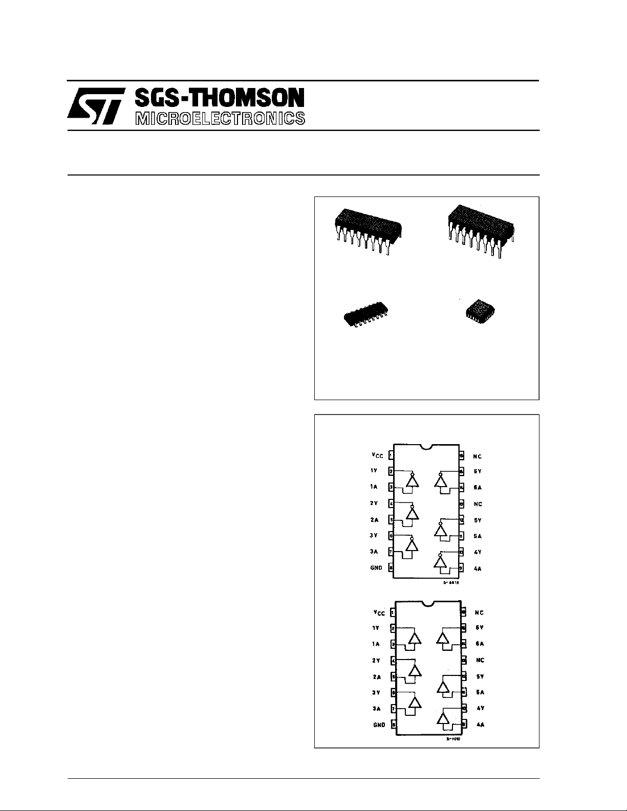
B1R
(Plastic Package)
M1R
(Micro Package)
ORDER CODES :
M54HC XXX X F 1R M74HCXXXXM1R
M74HC XXXXB1R M74HCXXXXC 1R
(Ceramic Package)
F1R
C1R
(Chip Carrier)
DESCRIPTION
The M54/74HC4049 and the M54/74HC4050 are
high speed CMOS HEX BUFFER fabricated in silicon gate C2MOS technology.
They have the same high speed performance of
LSTTL combined with true CMOS low power consumption.
The M54/75HC4049 is an invertingbuffer,whilethe
M54/74HC4050 is a non-inverting buffer.
The internal circuit is composed of 3 stage or 2stageinverters, whichprovides high noise immunity
and a stable output.
Input protection circuits are different from those of
the high speed CMOS IC’s.
The VCC side diodes are designed to allow logiclevel convertion from high-level voltages (up to
15 V) to low-level voltages.
PIN CONNECTIONS(top view)
HC4049
HC4050
NC =
No Internal
Connection
March1993
1/11
Page 2
M54/M74HC4049/ 4050
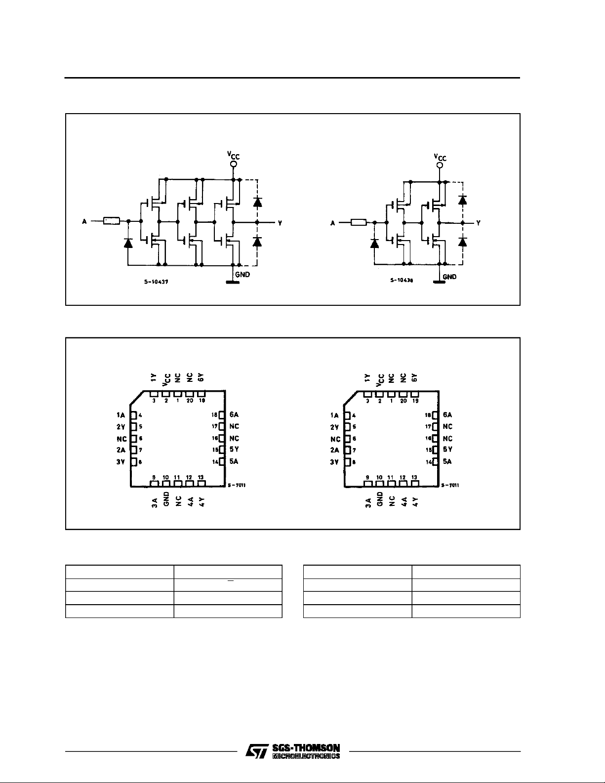
CIRCUIT SCHEMATIC (Per Gate)
HC4049 HC405 0
CHIP CARRIER
HC4049 HC405 0
NC =No InternalConnection
TRUTH TABLE (HC4049)
INPUT OUTPUT
nA nY
LH
HL
2/11
TRUTH TABLE (HC 4 050)
INPUT OUTPUT
nA nY
LL
HH
Page 3
M54/M74HC4049/4050
PIN DESCRIPTION (HC4049)
PIN No SYMBOL NAME AND FUNCTION
2, 4, 6, 10,
1Y to 6Y Data Outputs
12, 15
3, 5, 7, 9,
1A to 6A Data Inputs
11, 14
13, 16 NC Not Connected
8 GND Ground (0V)
1V
CC
Positive Supply Voltage
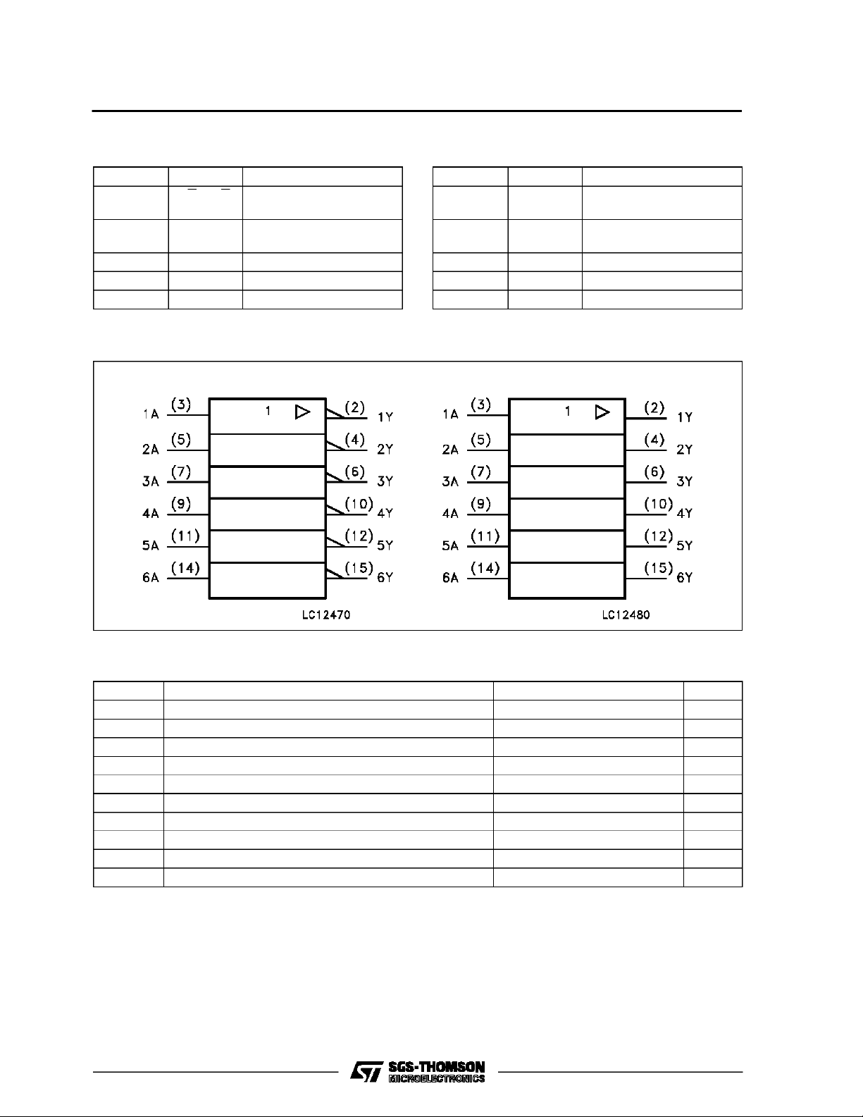
IEC LOGIC SYMBOLS
PIN DESCRIPTIO N (H C4050)
PIN No SYMBOL NAME AND FUNCTION
2, 4, 6, 10,
12, 15
3, 5, 7, 9,
11, 14
13, 16 NC Not Connected
8 GND Ground (0V)
1V
1Y to 6Y Data Outputs
1A to 6A Data Inputs
CC
Positive Supply Voltage
HC4050HC404 9
ABSOLU TE M AXI MU M R AT INGS
Symbol Parameter Value Unit
V
CC
V
V
O
I
IK
I
OK
I
O
I
or I
CC
P
D
T
stg
T
AbsoluteMaximumRatingsarethose values beyondwhichdamage tothedevicemayoccur. Functional operationunder these conditionisnotimplied.
(*)500 mW:≅ 65oC derate to300 mW by 10mW/oC: 65oCto85oC
Supply Voltage -0.5 to +7 V
DC Input Voltage -0.5 to VCC+ 0.5 V
I
DC Output Voltage -0.5 to VCC+ 0.5 V
DC Input Diode Current ± 20 mA
DC Output Diode Current ± 20 mA
DC Output Source Sink Current Per Output Pin ± 25 mA
DC VCCor Ground Current ± 50 mA
GND
Power Dissipation 500 (*) mW
Storage Temperature -65 to +150
Lead Temperature (10 sec) 300
L
o
C
o
C
3/11
Page 4
M54/M74HC4049/ 4050
RECO MM ENDED OPERAT IN G CONDI TI ONS
Symbol Parameter Value Unit
V
V
V
T
t
r,tf
DC SPECIFICATIO NS
Symbol Parameter
V
IH
V
V
OH
V
OL
I
I
CC
Supply Voltage 2 to 6 V
CC
Input Voltage 0 to V
I
Output Voltage 0 to V
O
Operating Temperature: M54HC Series
op
M74HC Series
CC
CC
-55 to +125
-40 to +85
Input Rise and Fall Time VCC= 2 V 0 to 1000 ns
V
= 4.5 V 0 to 500
CC
V
= 6 V 0 to 400
CC
Test Conditions Value
V
(V)
CC
=25oC
T
A
54HC and 74HC
-40 to 85oC
74HC
-55 to 125oC
Min. Typ. Max. Min. Max. Min. Max.
High Level Input
Voltage
2.0 1.5 1.5 1.5
4.5 3.15 3.15 3.15
6.0 4.2 4.2 4.2
Low Level Input
IL
Voltage
2.0 0.5 0.5 0.5
4.5 1.35 1.35 1.35
6.0 1.8 1.8 1.8
High Level
Output Voltage
Low Level Output
Voltage
Input Leakage
I
Current
Quiescent Supply
2.0
V
=
I
4.5 4.4 4.5 4.4 4.4
6.0 5.9 6.0 5.9 5.9
4.5 I
6.0 I
2.0
4.5 0.0 0.1 0.1 0.1
6.0 0.0 0.1 0.1 0.1
4.5 I
6.0 I
6.0
IO=-20 µA
V
IH
or
V
IL
=-6.0 mA 4.18 4.31 4.13 4.10
O
=-7.8 mA 5.68 5.8 5.63 5.60
O
V
=
I
IO=20µA
V
IH
or
V
IL
= 6.0 mA 0.17 0.26 0.33 0.40
O
= 7.8 mA 0.18 0.26 0.33 0.40
O
VI=VCCor GND
VI=15V
1.9 2.0 1.9 1.9
0.0 0.1 0.1 0.1
±0.1
±0.5
±1
±5
6.0 VI=VCCor GND 1 10 20 µA
Current
54HC
±1 µA
V
V
o
C
o
C
Unit
V
V
V
V
4/11
Page 5

M54/M74HC4049/4050
AC ELECTRICAL CHARACTERISTICS (CL=50pF,Inputtr=tf=6ns)
Test Conditions Value
T
=25oC
Symbol Parameter
t
t
TLH
THL
Output Transition
Time
V
C
CC
(V)
L
(pF)
2.0
50
4.5 7121518
A
54HC and 74HC
Min. Typ. Max. Min. Max. Min. Max.
25 60 75 90
6.0 6101315
t
PLH
t
PHL
Propagation
Delay Time
2.0
50
4.5 9151923
30 75 95 115
6.0 8131620
2.0
150
4.5 14 20 25 30
45 100 125 150
6.0 12 17 21 26
C
C
PD
Input Capacitance 5 10 10 10 pF
IN
(*) Power Dissipation
26
Capacitance
CPDisdefinedas thevalue oftheIC’sinternalequivalent capacitance whichiscalculated from the operating currentconsumption without load. (Refer
to Test Circuit).Averageoperting current can be obtained by the followingequation. ICC(opr) = CPD•VCC•fIN+ICC(perGate)
-40 to 85oC
74HC
-55 to 125oC
54HC
Unit
ns
ns
ns
pF
SWITCHING CHARACTERISTICS TEST WAVEFORM
HC4049
HC4050
5/11
Page 6

M54/M74HC4049/ 4050
TEST CIRCUIT ICC(Opr.)
HC4049 HC4050
INPUTWAVEFORM ISTHE SAMEAS THATINCASE OF SWITCHINGCHARACTERISTICSTEST.
6/11
Page 7

M54/M74HC4049/4050
Plastic DIP16 (0.25) MECHANICAL DATA
DIM.
MIN. TYP. MAX. MIN. TYP. MAX.
a1 0.51 0.020
B 0.77 1.65 0.030 0.065
b 0.5 0.020
b1 0.25 0.010
D 20 0.787
E 8.5 0.335
e 2.54 0.100
e3 17.78 0.700
F 7.1 0.280
I 5.1 0.201
L 3.3 0.130
Z 1.27 0.050
mm inch
P001C
7/11
Page 8

M54/M74HC4049/ 4050
Ceramic DIP16/1 MECHANICAL DATA
DIM.
MIN. TYP. MAX. MIN. TYP. MAX.
A 20 0.787
B 7 0.276
D 3.3 0.130
E 0.38 0.015
e3 17.78 0.700
F 2.29 2.79 0.090 0.110
G 0.4 0.55 0.016 0.022
H 1.17 1.52 0.046 0.060
L 0.22 0.31 0.009 0.012
M 0.51 1.27 0.020 0.050
N 10.3 0.406
P 7.8 8.05 0.307 0.317
Q 5.08 0.200
mm inch
8/11
P053D
Page 9

SO16 (Narrow) MECHANICAL DATA
M54/M74HC4049/4050
DIM.
MIN. TYP. MAX. MIN. TYP. MAX.
A 1.75 0.068
a1 0.1 0.2 0.004 0.007
a2 1.65 0.064
b 0.35 0.46 0.013 0.018
b1 0.19 0.25 0.007 0.010
C 0.5 0.019
c1 45° (typ.)
D 9.8 10 0.385 0.393
E 5.8 6.2 0.228 0.244
e 1.27 0.050
e3 8.89 0.350
F 3.8 4.0 0.149 0.157
G 4.6 5.3 0.181 0.208
L 0.5 1.27 0.019 0.050
M 0.62 0.024
S8°(max.)
mm inch
P013H
9/11
Page 10

M54/M74HC4049/ 4050
PLCC20 MECHANICAL DATA
DIM.
MIN. TYP. MAX. MIN. TYP. MAX.
A 9.78 10.03 0.385 0.395
B 8.89 9.04 0.350 0.356
D 4.2 4.57 0.165 0.180
d1 2.54 0.100
d2 0.56 0.022
E 7.37 8.38 0.290 0.330
e 1.27 0.050
e3 5.08 0.200
F 0.38 0.015
G 0.101 0.004
M 1.27 0.050
M1 1.14 0.045
mm inch
10/11
P027A
Page 11

M54/M74HC4049/4050
Information furnished is believed to be accurate and reliable. However, SGS-THOMSON Microelectronics assumes no responsability for the
consequences of use of such information nor for any infringement of patents or other rights of third parties which may results from its use. No
license isgranted by implication or otherwiseunder any patent orpatent rights of SGS-THOMSONMicroelectronics. Specificationsmentioned
in this publication are subject to change without notice. This publication supersedes and replaces all information previously supplied.
SGS-THOMSON Microelectronicsproductsare notauthorizedfor use ascritical componentsinlife supportdevices orsystems without express
written approval of SGS-THOMSON Microelectonics.
1994 SGS-THOMSON Microelectronics- All Rights Reserved
Australia - Brazil - France - Germany - Hong Kong - Italy - Japan - Korea - Malaysia - Malta - Morocco - The Netherlands -
Singapore - Spain - Sweden- Switzerland - Taiwan - Thailand - United Kingdom - U.S.A
SGS-THOMSON MicroelectronicsGROUP OF COMPANIES
11/11
 Loading...