

Page 1
.HIGH SPEED
tPD= 13 ns(TYP.) AT VCC=5V
.LOWPOWERDISSIPATION
ICC=4µA(MAX.) AT TA=25°C
.HIGH NOISEIMMUNITY
V
NIH=VNIL
=28%VCC(MIN.)
.OUTPUT DRIVE CAPABILITY
10 LSTTL LOADS
.SYMMETRICALOUTPUT IMPEDANCE
|IOH|= IOL=4mA (MIN.)
.BALANCEDPROPAGATION DELAYS
t
PLH=tPHL
.WIDE OPERATINGVOLTAGE RANGE
VCC(OPR)= 2 V TO 6 V
.PIN ANDFUNCTION COMPATIBLE
WITH 4024B
M54HC4024
M74HC4024
7 STAGE BINARY COUNTER
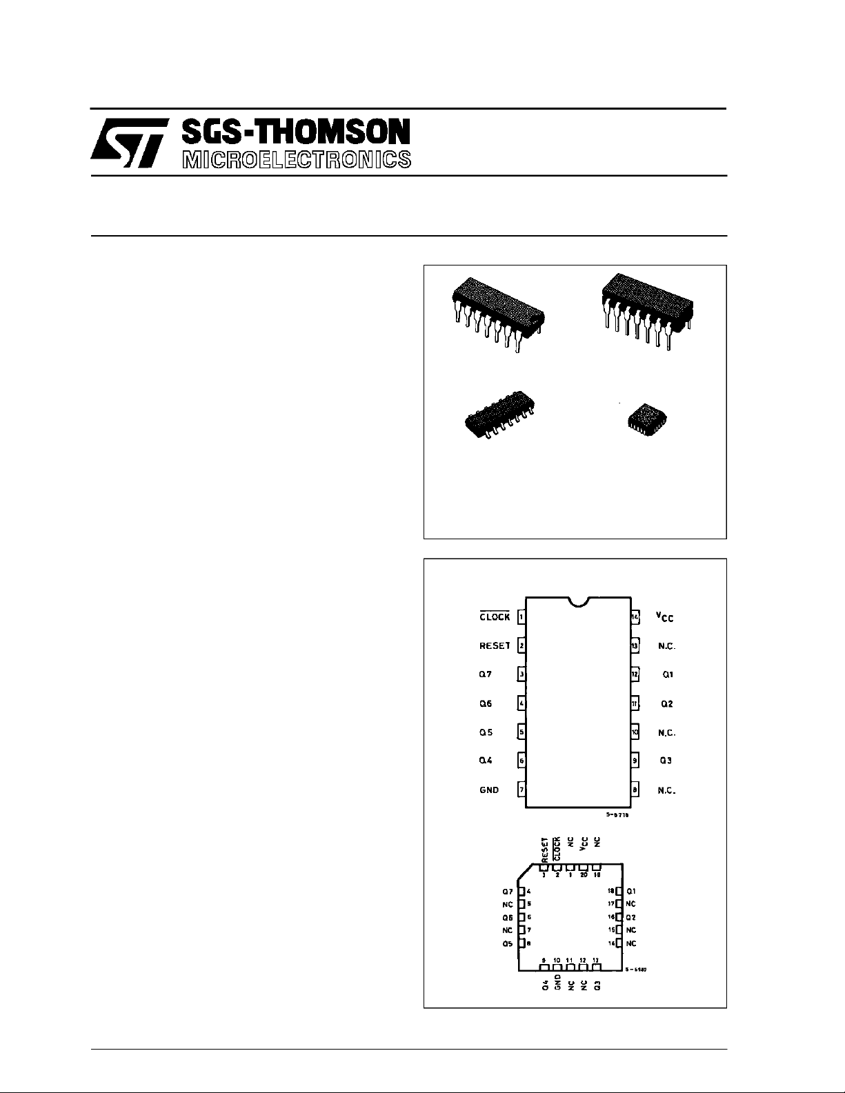
B1R
(PlasticPackage)
M1R
(MicroPackage)
ORDER CODES :
M54HC 4024F1R M74H C4024M1R
M74HC 4024B1R M74HC4 024C1R
F1R
(CeramicPackage)
C1R
(Chip Carrier)
DESCRIPTION
The M54/74HC4024 is a high speed CMOS 7STAGE BINARY COUNTER fabricated in silicon
gate C2MOS technology. It has the same high
speed performance of LSTTL combined with true
CMOS low power consumption. The HC4024is a 7
stage Counter. This devices is incremented on the
falling edge (negative transition) of the input clock,
andall itsoutputsarereset toalowlevelby applying
a logical high on their reset input. All inputs are
equipped with protection circuits against static discharge andtransient excess voltage.
PIN CONNECTIONS(top view)
NC =
No Internal
Connection
October 1992
1/11
Page 2
M54/M74HC4024
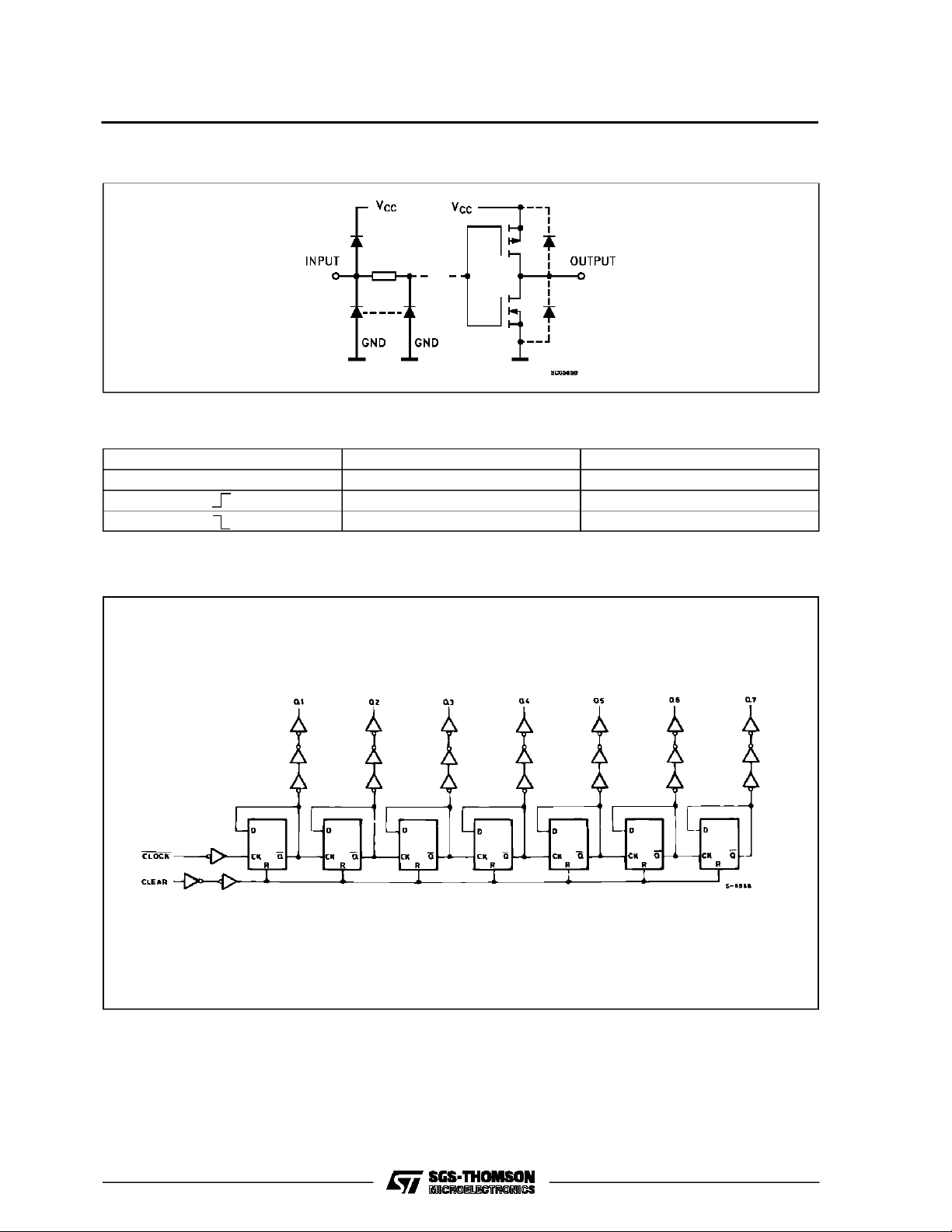
INPUT AND OUTPUT EQUIVALENT CIRCUIT
TRUTH TABLE
CLOCK CLEAR OUTPUT STATE
X H ALL OUTPUTS = ”L”
X:DON’TCARE
L NO CHANGE
L ADVANCE TO NEXT STATE
LOGIC DIAGRAM
2/11
Page 3
M54/M74HC4024
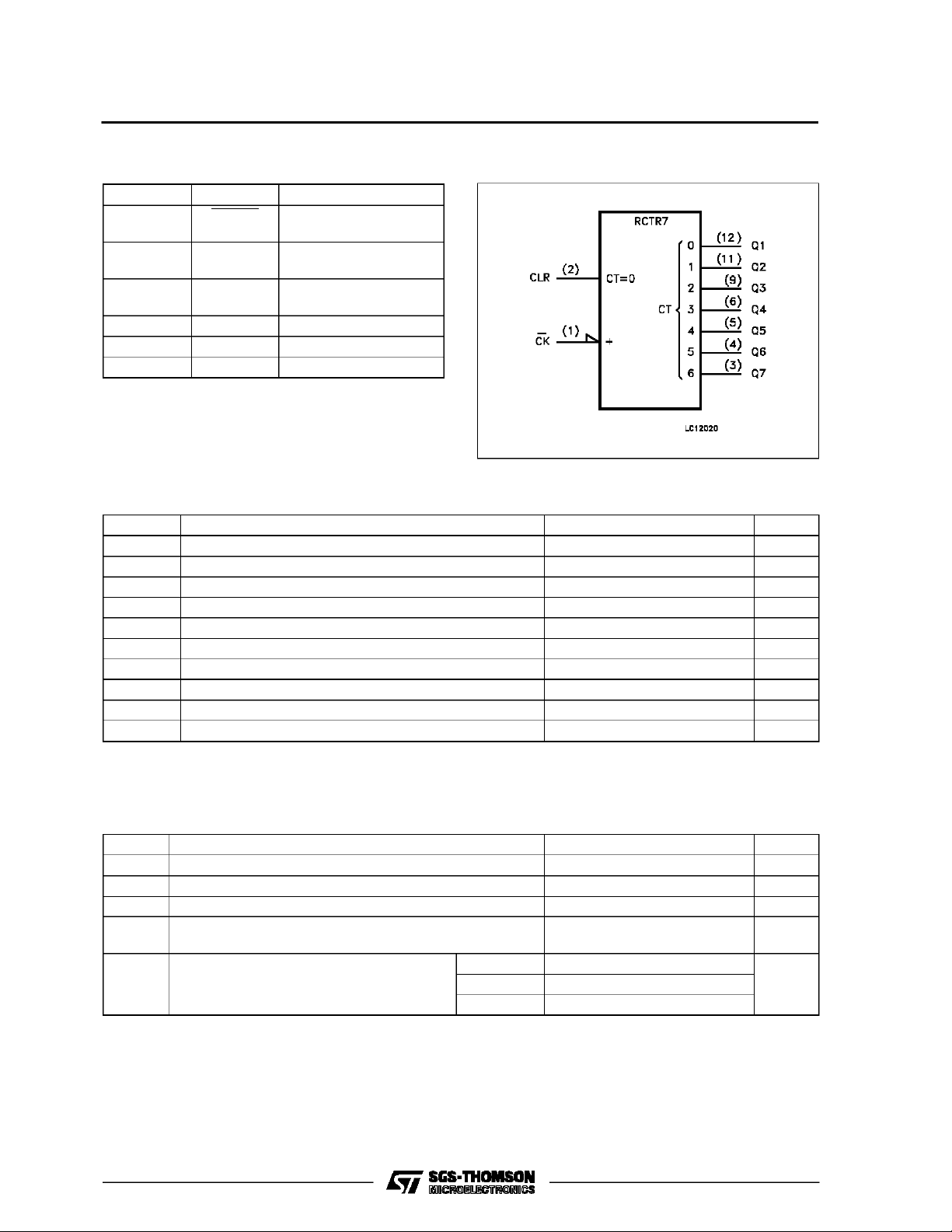
PIN DESCRIPTION
IEC LOGIC SYMBOL
PIN No SYMBOL NAME AND FUNCTION
1 CLOCK Clock Input (HIGH to
LOW, Edge-triggered)
2 RESET Reset Input (Active
HIGH)
12, 11, 9, 6,
Q1 to Q7 Parallel Outputs
5, 4, 3
8, 10, 13 NC Not Connected
7 GND Ground (0V)
14 V
CC
Positive Supply Voltage
ABSOLU TE MAXIMU M RAT INGS
Symbol Parameter Value Unit
V
CC
V
V
O
I
IK
I
OK
I
O
or I
I
CC
P
D
T
stg
T
AbsoluteMaximumRatingsarethose values beyond whichdamage tothedevicemayoccur. Functional operation under these conditionisnotimplied.
(*)500 mW: ≅ 65oC derateto300mWby 10mW/oC: 65oCto85oC
Supply Voltage -0.5 to +7 V
DC Input Voltage -0.5 to VCC+ 0.5 V
I
DC Output Voltage -0.5 to VCC+ 0.5 V
DC Input Diode Current ± 20 mA
DC Output Diode Current ± 20 mA
DC Output Source Sink Current Per Output Pin ± 25 mA
DC VCCor Ground Current ± 50 mA
GND
Power Dissipation 500 (*) mW
Storage Temperature -65 to +150
Lead Temperature (10 sec) 300
L
o
C
o
C
RECO MM ENDED OPERATI N G CONDI TIONS
Symbol Parameter Value Unit
V
T
t
V
V
r,tf
Supply Voltage 2 to 6 V
CC
Input Voltage 0 to V
I
Output Voltage 0 to V
O
Operating Temperature: M54HC Series
op
M74HC Series
CC
CC
-55 to +125
-40 to +85
Input Rise and Fall Time VCC= 2 V 0 to 1000 ns
V
= 4.5 V 0 to 500
CC
= 6 V 0 to 400
V
CC
V
V
o
C
o
C
3/11
Page 4
M54/M74HC4024
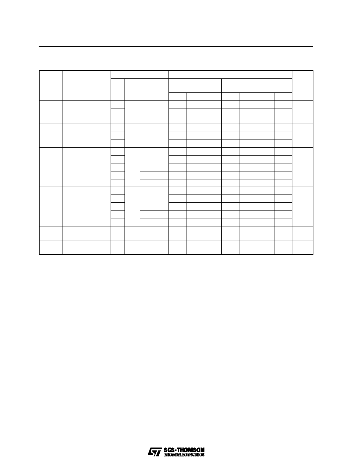
DC SPECIFICATIO NS
Symbol Parameter
V
V
V
V
I
High Level Input
IH
Voltage
Low Level Input
IL
Voltage
High Level
OH
Output Voltage
Low Level Output
OL
Voltage
I
Input Leakage
I
Current
Quiescent Supply
CC
Current
Test Conditions Value
V
(V)
CC
=25oC
A
54HC and 74HC
Min. Typ. Max. Min. Max. Min. Max.
-40 to 85oC
74HC
-55 to 125oC
54HC
Unit
T
2.0 1.5 1.5 1.5
4.5 3.15 3.15 3.15
6.0 4.2 4.2 4.2
2.0 0.5 0.5 0.5
4.5 1.35 1.35 1.35
6.0 1.8 1.8 1.8
2.0
4.5 4.4 4.5 4.4 4.4
6.0 5.9 6.0 5.9 5.9
4.5 I
6.0 I
2.0
4.5 0.0 0.1 0.1 0.1
6.0 0.0 0.1 0.1 0.1
4.5 I
6.0 I
6.0
=
V
I
IO=-20 µA
V
IH
or
V
IL
=-4.0 mA 4.18 4.31 4.13 4.10
O
=-5.2 mA 5.68 5.8 5.63 5.60
O
V
=
I
IO=20µA
V
IH
or
V
IL
= 4.0 mA 0.17 0.26 0.33 0.40
O
= 5.2 mA 0.18 0.26 0.33 0.40
O
VI=VCCor GND ±0.1 ±1 ±1 µA
1.9 2.0 1.9 1.9
0.0 0.1 0.1 0.1
6.0 VI=VCCor GND 4 40 80 µA
V
V
V
V
4/11
Page 5

M54/M74HC4024
AC ELECTRICAL CHARACTERISTICS (CL=50pF,Inputtr=tf=6ns)
Test Conditions Value
T
=25oC
Symbol Parameter
t
t
TLH
THL
Output Transition
Time
V
CC
(V)
2.0 30 75 95 110
4.5 8151922
A
54HC and 74HC
Min. Typ. Max. Min. Max. Min. Max.
6.0 7131619
t
PLH
t
PHL
Propagation
Delay Time
(Qn - Qn + 1)
t
PLH
t
PHL
Propagation
Delay Time
Clock - Q1
t
PHL
Propagation
Delay Time
(CLEAR - Qn)
f
MAX
Maximum Clock
Frequency
2.0 24 60 75 90
4.5 6121518
6.0 5101315
2.0 60 120 150 180
4.5 15 24 30 36
6.0 13 20 26 31
2.0 60 120 150 180
4.5 15 24 30 36
6.0 13 20 26 31
2.0 8 17 7 5.6
4.5 42 67 34 28
6.0 49 79 40 34
t
W(H)
t
W(L)
Minimum Pulse
Width (CLOCK)
2.0 24 75 95 110
4.5 6151922
6.0 5131619
t
W(H)
Minimum Pulse
Width (CLEAR)
2.0 32 75 95 110
4.5 8151922
6.0 7131619
t
REM
Minimum
Removal Time
2.0 25 30 40
4.5 5 6 8
6.0 5 5 7
C
C
PD
Input Capacitance 5 10 10 10 pF
IN
(*) Power Dissipation
34
Capacitance
(*) CPDisdefined as the value ofthe IC’sinternal equivalent capacitance whichis calculated fromthe operatingcurrentconsumption without load.
(Referto Test Circuit). Average operting current canbe obtained by the followingequation. ICC(opr) = CPD•VCC•fIN+I
-40 to 85oC
74HC
-55 to 125oC
54HC
CC
Unit
ns
ns
ns
ns
ns
ns
ns
ns
pF
5/11
Page 6

M54/M74HC4024
SWITCHING CHARACTERISTICS TEST WAVEFORM
TEST CIRCUIT ICC(Opr.)
INPUT WAVEFORMIS THE SAME AS THATIN CASEOF SWITCHINGCHARACTERISTICS TEST.
6/11
Page 7

Plastic DIP14 MECHANICAL DATA
M54/M74HC4024
DIM.
MIN. TYP. MAX. MIN. TYP. MAX.
a1 0.51 0.020
B 1.39 1.65 0.055 0.065
b 0.5 0.020
b1 0.25 0.010
D 20 0.787
E 8.5 0.335
e 2.54 0.100
e3 15.24 0.600
F 7.1 0.280
I 5.1 0.201
L 3.3 0.130
Z 1.27 2.54 0.050 0.100
mm inch
P001A
7/11
Page 8

M54/M74HC4024
Ceramic DIP14/1 MECHANICAL DATA
DIM.
MIN. TYP. MAX. MIN. TYP. MAX.
A 20 0.787
B 7.0 0.276
D 3.3 0.130
E 0.38 0.015
e3 15.24 0.600
F 2.29 2.79 0.090 0.110
G 0.4 0.55 0.016 0.022
H 1.17 1.52 0.046 0.060
L 0.22 0.31 0.009 0.012
M 1.52 2.54 0.060 0.100
N 10.3 0.406
P 7.8 8.05 0.307 0.317
Q 5.08 0.200
mm inch
8/11
P053C
Page 9

SO14 MECHANICAL DATA
M54/M74HC4024
DIM.
MIN. TYP. MAX. MIN. TYP. MAX.
A 1.75 0.068
a1 0.1 0.2 0.003 0.007
a2 1.65 0.064
b 0.35 0.46 0.013 0.018
b1 0.19 0.25 0.007 0.010
C 0.5 0.019
c1 45° (typ.)
D 8.55 8.75 0.336 0.344
E 5.8 6.2 0.228 0.244
e 1.27 0.050
e3 7.62 0.300
F 3.8 4.0 0.149 0.157
G 4.6 5.3 0.181 0.208
L 0.5 1.27 0.019 0.050
M 0.68 0.026
S8°(max.)
mm inch
P013G
9/11
Page 10

M54/M74HC4024
PLCC20 MECHANICAL DATA
DIM.
MIN. TYP. MAX. MIN. TYP. MAX.
A 9.78 10.03 0.385 0.395
B 8.89 9.04 0.350 0.356
D 4.2 4.57 0.165 0.180
d1 2.54 0.100
d2 0.56 0.022
E 7.37 8.38 0.290 0.330
e 1.27 0.050
e3 5.08 0.200
F 0.38 0.015
G 0.101 0.004
M 1.27 0.050
M1 1.14 0.045
mm inch
10/11
P027A
Page 11

M54/M74HC4024
Information furnishedis believed to be accurate and reliable. However, SGS-THOMSON Microelectronicsassumes no responsability for the
consequences of useof suchinformation nor forany infringement ofpatents or other rights of third parties which may results from its use. No
license is granted byimplication or otherwiseunder any patentor patent rights ofSGS-THOMSON Microelectronics. Specificationsmentioned
in this publication are subjectto changewithout notice. This publication supersedes andreplaces all information previously supplied.
SGS-THOMSON Microelectronicsproducts are not authorized foruse ascritical componentsinlife supportdevices or systemswithout express
written approval of SGS-THOMSON Microelectonics.
1994SGS-THOMSON Microelectronics- All Rights Reserved
Australia -Brazil - France - Germany - Hong Kong - Italy - Japan - Korea - Malaysia - Malta -Morocco - The Netherlands-
Singapore -Spain - Sweden- Switzerland - Taiwan - Thailand- UnitedKingdom - U.S.A
SGS-THOMSON Microelectronics GROUP OFCOMPANIES
11/11
 Loading...